EP0860727A2 - Dispositif pour commuter des images optiques entre des canaux differents - Google Patents
Dispositif pour commuter des images optiques entre des canaux differents Download PDFInfo
- Publication number
- EP0860727A2 EP0860727A2 EP98101113A EP98101113A EP0860727A2 EP 0860727 A2 EP0860727 A2 EP 0860727A2 EP 98101113 A EP98101113 A EP 98101113A EP 98101113 A EP98101113 A EP 98101113A EP 0860727 A2 EP0860727 A2 EP 0860727A2
- Authority
- EP
- European Patent Office
- Prior art keywords
- mirror
- plane
- optical
- imaging
- channels
- Prior art date
- Legal status (The legal status is an assumption and is not a legal conclusion. Google has not performed a legal analysis and makes no representation as to the accuracy of the status listed.)
- Granted
Links
Images

Classifications
-
- G—PHYSICS
- G02—OPTICS
- G02B—OPTICAL ELEMENTS, SYSTEMS OR APPARATUS
- G02B26/00—Optical devices or arrangements for the control of light using movable or deformable optical elements
- G02B26/08—Optical devices or arrangements for the control of light using movable or deformable optical elements for controlling the direction of light
- G02B26/0816—Optical devices or arrangements for the control of light using movable or deformable optical elements for controlling the direction of light by means of one or more reflecting elements
- G02B26/0833—Optical devices or arrangements for the control of light using movable or deformable optical elements for controlling the direction of light by means of one or more reflecting elements the reflecting element being a micromechanical device, e.g. a MEMS mirror, DMD
-
- H—ELECTRICITY
- H04—ELECTRIC COMMUNICATION TECHNIQUE
- H04N—PICTORIAL COMMUNICATION, e.g. TELEVISION
- H04N23/00—Cameras or camera modules comprising electronic image sensors; Control thereof
- H04N23/20—Cameras or camera modules comprising electronic image sensors; Control thereof for generating image signals from infrared radiation only
Definitions
- the invention relates to a device for switching from optical images between different channels.
- Such a device can e.g. serve different Parts of a visual field or otherwise different Objects with one optical system each in different to observe optical channels and the recorded Images in quick succession on a common optical Channel and e.g. an image resolution arranged therein Sensor. That would be the function of an "optical Multiplexers ".
- Such a device can also be used serve, a generated in the common optical channel Image successively towards different parallel channels conduct. That would be the function of an "optical Demultiplexers ".
- EP-A-0 469 293 describes a micromechanical Mirror system with a variety of electrical controllable mirror elements. A similar micromechanical mirror system is in EP-A-0 657 760 described.
- the invention has for its object a device for switching optical images between to create different optical channels.
- the switchover should be done at high speed to be possible. Image smearing should not occur. Switching between the optical channels should be in any sequence can be possible. The ones with big ones Masses or the need for a large numerical Aperture of optics related problems of the state of the art Technology should be avoided.
- each of the imaging optical systems in the switchable channels is e.g. a real picture of the associated level in the intermediate mapping level.
- the image is made out by the micromechanical mirror system one of the switchable channels in the common channel reflected and by the further optical system in the the level assigned to the common channel.
- the Intermediate image on the micromechanical mirror system acts as if for the other optical system self-illuminating image. Because on the micromechanical Mirror system creates a real image, no occur Interference. Switching from one of the switchable channels to another by appropriate Control of the mirror elements can be done very quickly and with any sequence of channels. Inertial forces are negligible. None occurs Image smear on. With the same optical arrangement can also change the direction of the radiation common channel successively assigned to the level the levels assigned to the individual switchable channels be mapped.
- Embodiments of the invention are the subject of Subclaims.
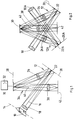
- 10 denotes an object, which in a Level 14 assigned to "switchable" optical channel 12 is arranged.
- Level 14 can e.g. in infinity lie.
- the plane 14 extends perpendicular to the optical one Axis 16 of a first imaging optical subsystem 18.
- the optical subsystem 18 is in Fig.1 as a lens shown.
- the first optical subsystem 18 forms the plane 14 in from a mirror plane 20 (or vice versa).
- a mirror grating 22 of parallel, mirror strips 24 inclined to the mirror plane 20 such a mirror grating is schematic in Fig.5 in shown on an enlarged scale.
- a second imaging optical subsystem 26 forms the Mirror plane 20 in an intermediate image plane 28 (or the other way around).
- the second imaging, optical Subsystem is also shown in Fig.1 as a lens.
- the mirror plane 20 and the intermediate image plane 28 are inclined towards each other.
- the mirror plane 20 and the Intermediate imaging plane 28 are also not perpendicular the optical axis of the second imaging optical Subsystem.
- the mirror plane 20, the second imaging, optical subsystem 26 and the intermediate imaging plane 28 are arranged so that the Scheimpflug condition is fulfilled: the mirror level 20 and the Intermediate image level 28 intersect with the Main level of the second imaging optical subsystem 26 in a straight line.
- the mirror grating 22 ensures that if this Scheimpflug condition is met, that of the first imaging optical subsystem 18 Imaging light bundle on the second imaging optical Subsystem is reflected. That way, it gets on the mirror grating 22 generated sharp real image of the Object is again sharp in the intermediate image plane 28 pictured.
- the sharp real image of the generated in the mirror plane Object 10 acts for the second imaging optical Subsystem 26 like a self-illuminating object. All Mirror strips 24 of the mirror grating are in the essentially in the focus of this figure.
- the Imaging light beam is directed towards the second imaging, optical subsystem reflected. Kick it no interference because in the plane of the mirror grille 22 a real image is generated.
- This micromechanical mirror system can, for example, in the manner of EP-A-0 469 mentioned above 293 or EP-A-0 657 760.
- the Mirror system 30 consists of a two-dimensional grid of mirror elements 34 (Fig. 3 and 4).
- the mirror elements 34 are known by a control circuit 32 and therefore not controllable in the manner shown. In the present embodiment, all mirror elements 34 driven in the same way.
- the further depicting Optical system 38 forms the micromechanical Mirror system 30 sharp in a plane 42.
- Level 42 is that assigned to the common optical channel 36 Level.
- the mirror elements 34 lie practically in the focus of the picture.
- the Mirror elements 34 are oriented so that they have the energy of the imaging light beam onto the other imaging optical system 38 guide.
- the beam direction can of course also be reversed: An object arranged in the plane 42 can be over Intermediate images in the intermediate image level 28 and the mirror plane 22 are shown in the plane 14.
- FIG. 1 shows the beam path for a channel 12 and the common channel 36. Similarly, except the channel 12 more channels through the micromechanical Mirror system 30 optionally with the common channel 36 optically connectable.
- Fig.2 shows the arrangement with two switchable channels 12 and 12A.
- the optical structure of the Channel 12A corresponds in mirror image to that of channel 12. Corresponding parts are the same in channel 12A As in channel 12, however, reference numerals have the addition Marked "A".
- the micromechanical mirror system 30 is for switching of the channels adjustable between two positions in the Figures 3 and 4 are shown.
- the imaging light beam is off the channel 12 passed into the common channel 36.
- the Layer 42 becomes the image of one of the imaging optics Subsystem 18 in the associated level 14 detected object generated.
- the Imaging beams from channel 12A into the common Channel 36 directed.
- the image becomes one of the imaging optical subsystem 18A in the associated one Level of the captured object.
- more than two switchable channels about the optical axis 40 of the imaging optical system 38 may be arranged around, for example two more Channels in the plane perpendicular to the paper plane of Fig. 2.
- a section along an optical axis 38 containing the plane perpendicular to the paper plane would then be the same look like Fig. 2.
- the mirror elements 34 of the The micromechanical mirror system must then have two axes be tiltable.
- the arrangement of the micromechanical mirror system 30 symmetrical to the optical axis 40 of the imaging, optical system 38 and the symmetrical arrangement of the Channels 12 and 12A occur when switching the different channels 12 and 12A no vignetting of the Imaging light bundle.
- Fig. 6 shows a "switchable" channel and the common one Channel in a modified version.
- an object 46 is in a Level 48 through an imaging optical system 50 in the Intermediate mapping level 28 mapped.
- the imaging optical system 50 here is a decentered optic. This allows a further intermediate image as in the "Mirror plane" of Fig. 1 and 2 are omitted.
- the level 48 goes directly to the intermediate image level 28 pictured.
- the micromechanical mirror system and the common channels correspond to those of Fig. 1 and 2. Corresponding parts are therefore the same in FIG Reference numerals as in Fig. 1 and 2.
- the imaging, optical system 50 forms a channel 52 of the "switchable" optical channels Several such switchable channels are around the optical axis 40 of the imaging optical system 38 arranged around.
- optical multiplexers or demultiplexers can find different applications.
- An image resolution sensor e.g. a Matrix detector can be arranged.
- the different switchable channels 12, 12A ... can then different sectors of an extended field of view observe. Via the micromechanical mirror system 30 can the different sectors in faster, if necessary, variable, sequential from that image-resolution sensor can be detected.
- variable thermal images e.g. a quick to simulate moving, hot target.
- the production rapidly changing thermal images is difficult. Temperatures of the surface elements representing the thermal image cannot be changed quickly.
- the device acts as "optical multiplexer".
Landscapes
- Physics & Mathematics (AREA)
- Engineering & Computer Science (AREA)
- Multimedia (AREA)
- Signal Processing (AREA)
- General Physics & Mathematics (AREA)
- Optics & Photonics (AREA)
- Mechanical Light Control Or Optical Switches (AREA)
- Studio Devices (AREA)
- Use Of Switch Circuits For Exchanges And Methods Of Control Of Multiplex Exchanges (AREA)
Applications Claiming Priority (2)
| Application Number | Priority Date | Filing Date | Title |
|---|---|---|---|
| DE19707432 | 1997-02-25 | ||
| DE19707432A DE19707432A1 (de) | 1997-02-25 | 1997-02-25 | Vorrichtung zur Umschaltung von optischen Bildern zwischen verschiedenen Kanälen |
Publications (3)
| Publication Number | Publication Date |
|---|---|
| EP0860727A2 true EP0860727A2 (fr) | 1998-08-26 |
| EP0860727A3 EP0860727A3 (fr) | 1998-10-07 |
| EP0860727B1 EP0860727B1 (fr) | 2003-08-13 |
Family
ID=7821367
Family Applications (1)
| Application Number | Title | Priority Date | Filing Date |
|---|---|---|---|
| EP98101113A Expired - Lifetime EP0860727B1 (fr) | 1997-02-25 | 1998-01-23 | Dispositif pour commuter des images optiques entre des canaux differents |
Country Status (3)
| Country | Link |
|---|---|
| US (1) | US5936759A (fr) |
| EP (1) | EP0860727B1 (fr) |
| DE (2) | DE19707432A1 (fr) |
Families Citing this family (21)
| Publication number | Priority date | Publication date | Assignee | Title |
|---|---|---|---|---|
| WO1999041007A2 (fr) * | 1998-02-11 | 1999-08-19 | University Of Houston | Procede et appareil pour induire des reactions biochimiques au moyen de reactifs photogeneres |
| US20040035690A1 (en) * | 1998-02-11 | 2004-02-26 | The Regents Of The University Of Michigan | Method and apparatus for chemical and biochemical reactions using photo-generated reagents |
| US6271957B1 (en) * | 1998-05-29 | 2001-08-07 | Affymetrix, Inc. | Methods involving direct write optical lithography |
| WO2001014924A1 (fr) | 1999-08-26 | 2001-03-01 | The Ohio State University | Dispositif de production de retards incrementiels controles sur le plan optique |
| US6388815B1 (en) | 2000-08-24 | 2002-05-14 | The Ohio State University | Device and method for producing optically-controlled incremental time delays |
| US7800639B2 (en) * | 2001-02-15 | 2010-09-21 | Joseph Dale Udy | Laser pulse image switches |
| US20020110349A1 (en) * | 2001-02-15 | 2002-08-15 | Udy Joseph D. | Minuscule images of alphanumeric symbols |
| US6760140B1 (en) | 2002-03-01 | 2004-07-06 | The Ohio State University Research Foundation | Binary optical interconnection |
| US6674939B1 (en) | 2002-03-26 | 2004-01-06 | The Ohio State University | Using fibers as delay elements in optical true-time delay devices based on the white cell |
| US6724951B1 (en) | 2002-03-26 | 2004-04-20 | The Ohio State University | Using fibers as shifting elements in optical interconnection devices based on the white cell |
| US6766073B1 (en) | 2002-05-17 | 2004-07-20 | The Ohio State University | Optical circulator with large number of ports and no polarization-based components |
| US6958861B1 (en) * | 2002-12-02 | 2005-10-25 | The Ohio State University | Method and apparatus for combining optical beams |
| US7236238B1 (en) | 2002-12-02 | 2007-06-26 | The Ohio State University | Method and apparatus for monitoring the quality of optical links |
| DE102004024313A1 (de) * | 2004-05-15 | 2005-12-08 | Diehl Bgt Defence Gmbh & Co. Kg | Vorrichtung und Verfahren zur Abbildung einer Objektszene auf einer Detektoranordnung |
| US7633670B2 (en) * | 2004-07-16 | 2009-12-15 | The Ohio State University | Methods, systems, and devices for steering optical beams |
| US7430347B2 (en) * | 2004-07-16 | 2008-09-30 | The Ohio State University | Methods, systems, and apparatuses for optically generating time delays in signals |
| US20060034567A1 (en) * | 2004-07-16 | 2006-02-16 | Anderson Betty L | Optical beam combiner |
| DE102005018482A1 (de) * | 2005-04-21 | 2006-11-02 | Diehl Bgt Defence Gmbh & Co. Kg | Vorrichtung zur Abbildung eines Blickfelds auf einen Detektor |
| US7630598B2 (en) | 2006-05-10 | 2009-12-08 | The Ohio State University | Apparatus and method for providing an optical cross-connect |
| US7911671B2 (en) * | 2006-05-10 | 2011-03-22 | The Ohio State University | Apparatus and method for providing true time delay in optical signals using a Fourier cell |
| EP3186661B1 (fr) | 2014-08-26 | 2021-04-07 | Massachusetts Institute of Technology | Procédés et appareil pour l'imagerie tridimensionnelle (3d) |
Family Cites Families (13)
| Publication number | Priority date | Publication date | Assignee | Title |
|---|---|---|---|---|
| DE3330496C2 (de) * | 1983-08-24 | 1985-08-22 | Messerschmitt-Bölkow-Blohm GmbH, 8012 Ottobrunn | Einrichtung zur Lenkung eines Flugkörpers in ein Ziel |
| US5049740A (en) * | 1984-12-26 | 1991-09-17 | Hughes Aircraft Company | Multiple field of view sensor |
| US5119454A (en) * | 1988-05-23 | 1992-06-02 | Polaroid Corporation | Bulk optic wavelength division multiplexer |
| US5444572A (en) * | 1992-11-27 | 1995-08-22 | Lockheed Missiles & Space Company, Inc. | Wavefront corrector for scanning microlens arrays |
| US5448395A (en) * | 1993-08-03 | 1995-09-05 | Northrop Grumman Corporation | Non-mechanical step scanner for electro-optical sensors |
| DE4337047B4 (de) * | 1993-10-29 | 2004-11-25 | BODENSEEWERK GERäTETECHNIK GMBH | Passive bildauflösende Detektoranordnung |
| US5452024A (en) * | 1993-11-01 | 1995-09-19 | Texas Instruments Incorporated | DMD display system |
| DE4338390C2 (de) * | 1993-11-10 | 2001-06-13 | Bodenseewerk Geraetetech | Szenensimulator, insbesondere zum Testen von Infrarot-Sensoren in Zielsuchköpfen |
| US5557431A (en) * | 1993-12-16 | 1996-09-17 | Hughes Aircraft Company | Real-time compensated imaging system and method using a double-pumped phase-conjugate mirror |
| DE4402775C1 (de) * | 1994-01-27 | 1995-07-20 | Mannesmann Ag | Abbildungssystem mit elektronischem Bildsensor |
| US5691836A (en) * | 1995-07-11 | 1997-11-25 | Sy Technology, Inc. | Optically addressed spatial light modulator and method |
| US5640479A (en) * | 1995-10-18 | 1997-06-17 | Palomar Technologies Corporation | Fiberoptic face plate stop for digital micromirror device projection system |
| US5726795A (en) * | 1996-10-30 | 1998-03-10 | Hughes Electronics | Compact phase-conjugate mirror utilizing four-wave mixing in a loop configuration |
-
1997
- 1997-02-25 DE DE19707432A patent/DE19707432A1/de not_active Withdrawn
-
1998
- 1998-01-23 EP EP98101113A patent/EP0860727B1/fr not_active Expired - Lifetime
- 1998-01-23 DE DE59809240T patent/DE59809240D1/de not_active Expired - Fee Related
- 1998-02-23 US US09/027,910 patent/US5936759A/en not_active Expired - Fee Related
Also Published As
| Publication number | Publication date |
|---|---|
| DE19707432A1 (de) | 1998-08-27 |
| DE59809240D1 (de) | 2003-09-18 |
| EP0860727A3 (fr) | 1998-10-07 |
| EP0860727B1 (fr) | 2003-08-13 |
| US5936759A (en) | 1999-08-10 |
Similar Documents
| Publication | Publication Date | Title |
|---|---|---|
| EP0860727B1 (fr) | Dispositif pour commuter des images optiques entre des canaux differents | |
| DE69819860T2 (de) | System zur bidirektionellen abtastung | |
| EP1711777B2 (fr) | Procede pour determiner la position et le mouvement relativ d'un objet dans un espace | |
| DE4338390A1 (de) | Szenensimulator, insbesondere zum Testen von Infrarot-Sensoren in Zielsuchköpfen | |
| DE10038622A1 (de) | Scan-Mikroskop,optische Anordnung und Verfahren zur Bildaufnahme in der Scan-Mikroskopie | |
| DE69315575T2 (de) | Detektor kalibrierung | |
| EP1359452A1 (fr) | Microscope confocale avec deux réseaux de micro-lentilles et un réseau de diaphragmes | |
| DE60215223T2 (de) | Satellitengestütztes optisches beobachtungsinstrument mit zwei teleskopen | |
| DE19750947A1 (de) | Videokamera mit Ablenkungseinrichtung zur Erhöhung der Auflösung | |
| EP0905539B1 (fr) | Dispositif d'acquisition d'une pluralité de champ de vision à l'aide d'un détecteur de résolution d'image | |
| DE19608632A1 (de) | Vorrichtung und Verfahren zur optischen Abtastung von Oberflächen | |
| DE60014944T2 (de) | Vorrichtung zur bestimmung der räumlichen verteilung der spektralen emission eines objekts | |
| EP1649256A1 (fr) | Dispositif de mesure de temperature sans contact | |
| EP0452822B1 (fr) | Microscope d'opération pour au moins deux chirurgiens | |
| DE3412046C2 (fr) | ||
| EP0118057B1 (fr) | Procédé et appareil servant à balayer opto-mécanique de deux champs visuels | |
| DE102009001202B3 (de) | Kamerasystem mit Augenfinder-Modulen | |
| DE69108974T2 (de) | Abbildungs- und Überwachungsvorrichtung mit Matrixsensor. | |
| DE2056812B2 (de) | Vorrichtung zum Abtasten eines von der Erdoberfläche ausgehenden Abtaststrahls | |
| EP0916971B1 (fr) | Système microoptique commutable de déviation de faisceau | |
| CH689406A5 (de) | Stereoskopische Bildaufnahmevorrichtung. | |
| DE10030196C2 (de) | Anordnung und Verfahren zur Aufnahme von mehreren Ansichten einer Szene oder eines Gegenstandes | |
| DE19921374C2 (de) | Vorrichtung zur dreidimensionalen optischen Untersuchung eines Objektes mit Beleuchtung durch eine Lochplatte | |
| DE2841779C2 (de) | Vorrichtung zur Gesichtsfeldumschaltung bei einem optisch-mechanischen Abtastsystem | |
| DE4414287A1 (de) | Verfahren, Vorrichtung und Shearing-Element für die Shearing-Speckle-Interferometrie |
Legal Events
| Date | Code | Title | Description |
|---|---|---|---|
| PUAI | Public reference made under article 153(3) epc to a published international application that has entered the european phase |
Free format text: ORIGINAL CODE: 0009012 |
|
| PUAL | Search report despatched |
Free format text: ORIGINAL CODE: 0009013 |
|
| AK | Designated contracting states |
Kind code of ref document: A2 Designated state(s): DE FR GB |
|
| AX | Request for extension of the european patent |
Free format text: AL;LT;LV;MK;RO;SI |
|
| AK | Designated contracting states |
Kind code of ref document: A3 Designated state(s): AT BE CH DE DK ES FI FR GB GR IE IT LI LU MC NL PT SE |
|
| 17P | Request for examination filed |
Effective date: 19980926 |
|
| AKX | Designation fees paid |
Free format text: DE FR GB |
|
| GRAH | Despatch of communication of intention to grant a patent |
Free format text: ORIGINAL CODE: EPIDOS IGRA |
|
| GRAH | Despatch of communication of intention to grant a patent |
Free format text: ORIGINAL CODE: EPIDOS IGRA |
|
| GRAA | (expected) grant |
Free format text: ORIGINAL CODE: 0009210 |
|
| AK | Designated contracting states |
Designated state(s): DE FR GB |
|
| REG | Reference to a national code |
Ref country code: GB Ref legal event code: FG4D Free format text: NOT ENGLISH |
|
| REF | Corresponds to: |
Ref document number: 59809240 Country of ref document: DE Date of ref document: 20030918 Kind code of ref document: P |
|
| GBT | Gb: translation of ep patent filed (gb section 77(6)(a)/1977) |
Effective date: 20031009 |
|
| ET | Fr: translation filed | ||
| PLBE | No opposition filed within time limit |
Free format text: ORIGINAL CODE: 0009261 |
|
| STAA | Information on the status of an ep patent application or granted ep patent |
Free format text: STATUS: NO OPPOSITION FILED WITHIN TIME LIMIT |
|
| 26N | No opposition filed |
Effective date: 20040514 |
|
| RIN2 | Information on inventor provided after grant (corrected) |
Inventor name: BUETTNER, KNUT |
|
| PGFP | Annual fee paid to national office [announced via postgrant information from national office to epo] |
Ref country code: FR Payment date: 20061215 Year of fee payment: 10 |
|
| PGFP | Annual fee paid to national office [announced via postgrant information from national office to epo] |
Ref country code: GB Payment date: 20070117 Year of fee payment: 10 |
|
| PGFP | Annual fee paid to national office [announced via postgrant information from national office to epo] |
Ref country code: DE Payment date: 20070320 Year of fee payment: 10 |
|
| GBPC | Gb: european patent ceased through non-payment of renewal fee |
Effective date: 20080123 |
|
| PG25 | Lapsed in a contracting state [announced via postgrant information from national office to epo] |
Ref country code: DE Free format text: LAPSE BECAUSE OF NON-PAYMENT OF DUE FEES Effective date: 20080801 |
|
| REG | Reference to a national code |
Ref country code: FR Ref legal event code: ST Effective date: 20081029 |
|
| PG25 | Lapsed in a contracting state [announced via postgrant information from national office to epo] |
Ref country code: GB Free format text: LAPSE BECAUSE OF NON-PAYMENT OF DUE FEES Effective date: 20080123 |
|
| PG25 | Lapsed in a contracting state [announced via postgrant information from national office to epo] |
Ref country code: FR Free format text: LAPSE BECAUSE OF NON-PAYMENT OF DUE FEES Effective date: 20080131 |