EP0860762A2 - Circuit et méthode pour générer une tension de sortie continue - Google Patents
Circuit et méthode pour générer une tension de sortie continue Download PDFInfo
- Publication number
- EP0860762A2 EP0860762A2 EP98101782A EP98101782A EP0860762A2 EP 0860762 A2 EP0860762 A2 EP 0860762A2 EP 98101782 A EP98101782 A EP 98101782A EP 98101782 A EP98101782 A EP 98101782A EP 0860762 A2 EP0860762 A2 EP 0860762A2
- Authority
- EP
- European Patent Office
- Prior art keywords
- voltage
- input
- batt
- supply voltage
- output
- Prior art date
- Legal status (The legal status is an assumption and is not a legal conclusion. Google has not performed a legal analysis and makes no representation as to the accuracy of the status listed.)
- Withdrawn
Links
Images


Classifications
-
- G—PHYSICS
- G05—CONTROLLING; REGULATING
- G05F—SYSTEMS FOR REGULATING ELECTRIC OR MAGNETIC VARIABLES
- G05F1/00—Automatic systems in which deviations of an electric quantity from one or more predetermined values are detected at the output of the system and fed back to a device within the system to restore the detected quantity to its predetermined value or values, i.e. retroactive systems
- G05F1/10—Regulating voltage or current
- G05F1/46—Regulating voltage or current wherein the variable actually regulated by the final control device is DC
- G05F1/462—Regulating voltage or current wherein the variable actually regulated by the final control device is DC as a function of the requirements of the load, e.g. delay, temperature, specific voltage/current characteristic
- G05F1/465—Internal voltage generators for integrated circuits, e.g. step down generators
-
- G—PHYSICS
- G05—CONTROLLING; REGULATING
- G05F—SYSTEMS FOR REGULATING ELECTRIC OR MAGNETIC VARIABLES
- G05F3/00—Non-retroactive systems for regulating electric variables by using an uncontrolled element, or an uncontrolled combination of elements, such element or such combination having self-regulating properties
- G05F3/02—Regulating voltage or current
- G05F3/08—Regulating voltage or current wherein the variable is DC
- G05F3/10—Regulating voltage or current wherein the variable is DC using uncontrolled devices with non-linear characteristics
- G05F3/16—Regulating voltage or current wherein the variable is DC using uncontrolled devices with non-linear characteristics being semiconductor devices
- G05F3/18—Regulating voltage or current wherein the variable is DC using uncontrolled devices with non-linear characteristics being semiconductor devices using Zener diodes
-
- G—PHYSICS
- G05—CONTROLLING; REGULATING
- G05F—SYSTEMS FOR REGULATING ELECTRIC OR MAGNETIC VARIABLES
- G05F5/00—Systems for regulating electric variables by detecting deviations in the electric input to the system and thereby controlling a device within the system to obtain a regulated output
Definitions
- the invention relates to a circuit arrangement for generating a DC supply voltage as a function of an input DC voltage according to the preamble of claim 1 and a Method for generating a DC supply voltage for a signal generator unit according to claim 7.
- Such circuit arrangements are used to e.g. Sensors with downstream signaling unit with a voltage that is designed so that fluctuations in the DC input voltage Functionality of the unit to be supplied is not endangered. It has The voltage difference with which the Supply voltage for the consumer below the input voltage is, as shown in Figure 1, up to a first value of the input voltage to keep to a first, constant value and from one certain value of the input voltage to a second larger value to keep constant. In the intermediate transition area, in Normal operation, the supply voltage remains constant and is regardless of the input voltage.
- DE 41 31 170 A teaches a device in which means a Zener diode (Z diode) and a comparator and a controllable Current source a supply voltage is generated, which is in Intervals changes depending on the input voltage.
- Z diode Zener diode
- a comparator a comparator
- a controllable Current source a supply voltage is generated, which is in Intervals changes depending on the input voltage.
- This arrangement also proves due to its complexity, especially the controllable power source, as too complex and expensive.
- the supply voltage is a non-constant DC input voltage, for example a battery, won and for the Signaling unit provided.
- a preferred area of application for such methods is the coupling of decentralized sensor systems with central control electronics in motor vehicles, where the outsourced sensors and the associated signal generator units no longer directly from the vehicle electrical system voltage, but instead indirectly supplied by the central control unit using a current interface will.
- the changes in current are made by the central control unit of the power supply line to the outsourced signal generator unit.
- the object of the invention is to produce a circuit arrangement specify a DC supply voltage with that described above DC supply voltage curve as a function of the DC input voltage can be achieved in a simple manner.
- the task is furthermore, a method for generating a DC supply voltage to show for a signaling unit in which fluctuations in DC input voltage largely does not transmit the current signal hinder.
- the task is through the features of claim 1 for the Circuit arrangement and solved by claim 7 for the method.
- the circuit arrangement generates the desired profile of the DC supply voltage depending on the input DC voltage by means of a surprisingly simple circuit arrangement based on two zener diode arrays.
- Advantageous developments of the invention are described in claims 2 to 6. These describe in particular the dimensioning of the individual components.
- the control loop tracking according to claim 5 enables a non-reactive Current decoupling of the circuit arrangement.
- a DC supply voltage is provided, which over a Control circuit the DC supply voltage at the connection to the signal generator unit tracks the generated DC supply voltage without retroactive effect.
- Three connected input voltage intervals are preferred distinguished.
- the DC supply voltage of the input DC voltage is increased by one constant first amount reduced tracking, resulting in an emergency operation the signaling unit is guaranteed and also the Evaluation circuit can evaluate the signals of the signal generator unit, too if these are reduced.
- a subsequent second Voltage interval becomes the supply voltage with a constant nominal amount provided. This means that voltage compensation takes place for the normal operating state. However, if the DC input voltage exceeds this second voltage interval, follows DC supply voltage reduced by a second constant amount the input DC voltage.
- the inventive solution also ensures outside the compensated voltage range in normal operation defined states on the signaling unit and thus a the best possible maintenance of the operation of the signaling unit and the evaluation circuit, for example in the event of input voltage fluctuations.
- This Methods so advantageous for signal transmission by means of the signal stream can be extremely simple and effective through the circuit arrangement Realize according to one of claims 1 to 5, and in principle also other circuit arrangements, such as from the not yet disclosed Patent application DE 196 07 802 (EP 0 793 159) for generating the three Voltage intervals can be used.
- This circuitry then need to proceed according to the characteristics of claim 7 in the control loop, the output voltage at the connection to the signal generator unit (Sat) of the generated DC supply voltage tracks and ensures freedom of feedback.
- FIG. 1 shows the three voltage intervals I 1 , I 2 , I 3 of the input DC voltage U batt and the assigned supply voltage U out on the output side.
- the first interval I 1 the DC supply voltage of the input DC voltage U batt is tracked reduced by a constant first amount ⁇ U 1 in this area.
- the supply voltage U out is maintained at the desired nominal voltage Unom.
- an output voltage U out is generated in the voltage interval I 3 , which follows the input voltage U batt reduced by a second constant amount ⁇ U 2 .
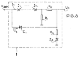
- the possible circuitry implementation is explained in more detail in connection with FIGS. 3 and 5.
- FIG. 1 first generates the DC supply voltage U z from the DC input voltage, while the control circuit 2 produces the output voltage U out at the connection to the unit to be supplied (for example a signal transmitter unit (Sat), see exemplary embodiment according to FIG 3) the DC supply voltage U z generated by the circuit arrangement 1 leads to.
- a signal transmitter unit see exemplary embodiment according to FIG 3
- the current pulses I signal generated by the signal transmitter unit Sat in the exemplary embodiment explained in more detail in FIG. 3 do not lead to fluctuations in the applied output voltage U out , since the interposed control circuit 2 immediately compensates for this, without having any effect on the circuit arrangement 1.
- Figures 3 and 5 show the input with the non-compensated, non-constant input DC voltage U Batt , for example a connection to a car battery.
- I 1 there is a first current path I 1 and a second current path I 2 parallel to it.
- I 1 a number n of diodes D 1 ... D n connected in series are arranged poled in the forward direction, the number n of diodes D determining the first constant amount ⁇ U 1 .
- these are connected to ground via a first resistor R 1 , so that a diode current is created which is so large that the diodes D 1 ...
- the last diode in FIG. 3 D 2 , in FIG. 5 D n
- the last diode is connected to the output of the DC supply voltage U z via a second, high-resistance resistor R 2 .
- the output of the DC supply voltage U z is connected to ground via a third resistor R 3 and a second Z-diode arrangement Z 2 in series therewith.
- the Zener voltage of the Z 2 is the DC supply voltage U z is reduced by the voltage drop U D via the diodes D 1 ... D n constant for the input DC voltage U Batt tracked until reaching. If the input DC voltage U Batt now exceeds the value of Z 2 , the second Zener diode Z 2 becomes conductive. The current through the diodes D 1 ... D n can thus flow to ground both via the resistor R 1 and in parallel to it through the series arrangement of R 2 , R 3 and Z 2 .
- a voltage divider is formed from the resistors R 2 and R 3 , with R 2 being chosen to be higher by a factor of 100 than R 3 by a factor of 100, so that a change in voltage of the input DC voltage U Batt is smaller by a factor of 100 and is therefore not detectable by D 1. .D n works. Compensation for the DC input voltage changes, e.g. the battery voltage fluctuations, is achieved. However, if the input DC voltage U Batt exceeds a value which is around UZ 2 plus UZ 1 , the first Zener diode Z 1 in the second current path I 2 also becomes conductive. This bridges the diodes and the resistor R 2 . The voltage divider between R 2 and R 3 is eliminated.
- the DC supply voltage U z now follows in a second constant amount ⁇ U 2 of the input DC voltage U Batt , the second amount ⁇ U 2 being largely determined by the voltage UZ 1 .
- the Zener diode arrangements Z 1 and Z 2 can be implemented both simple Z diodes and temperature compensated Zener diode arrangements, for example by connecting them in series with temperature compensating diodes with correspondingly different temperature coefficients.
- the desired dependency of the DC supply voltage U z on the applied DC input voltage U batt arises .
- this embodiment of the circuit arrangement according to FIG. 5 can also be used advantageously for other uses than that shown in FIG. 3, that is to say without a signal transmitter unit for current signaling and an associated evaluation circuit or the control circuit 2, due to its simplicity.
- circuit arrangement discussed 1 shows the overall arrangement according to FIG. 3, this shows the preferred use the circuit arrangement for the voltage supply of a signal generator unit Sat, which is controlled via a control circuit 2.
- a control circuit 2 instead of the particularly preferred embodiment of the circuit arrangement 5 could in principle also be another suitable one Circuit arrangement, for example in DE 196 07 802 (EP 0 793 159) described, can be arranged before the control loop 2, the design 5 already described Has advantages.
- the control circuit 2 compares the output voltage U out with the DC supply voltage U z present on the input side.
- the signal transmitter unit Sat has a closed-circuit current path I R and a signal current path I signal . As is known, this can be achieved, for example, by switchable signal loads.
- the evaluation circuit I mess is arranged between the control circuit 2 and the recompensated input of the circuit arrangement 1 which is at U batt and is formed via a current mirror, formed from the transistors T 2 and T 3 , as well as the resistors RM 1 and RM 2 and a constant current source the signal sent by the transmitter unit satellite signal current I evaluates signal by a comparator K 2 compares the voltage drops across the resistors RM 1 and RM 2 and the output signal S passes to further processing, for example to a microprocessor.
- the control circuit 2 is formed from a comparator K 1 , at the output of which there is the resistor R K and the transistor T K , the transistor T K being connected as a series transistor with the base to the comparator K 1 and with the emitter to the signaling unit Sat.
- the DC supply voltage U z generated by the circuit arrangement 1 is compared in the comparator K 1 with U out and U out is readjusted accordingly.
- the current pulses I signal in the amount of 40 mA for signal transmission, which are considerable in this exemplary embodiment, act, decoupled by the control circuit 2, not on the supply voltage-generating circuit arrangement 1.
- the current pulses I signal are conducted quasi unaffected by the transistor TK to the current measuring evaluation circuit I mess and recognized there.
- the voltage across the evaluation circuit I mess is the difference between the DC input voltage U Batt and the output voltage U out at the signal generator unit Sat and the voltage drop across the transistor TK.
- the difference is limited by the method used and is therefore approximately between the amounts ⁇ U 1 and ⁇ U 2 .
- the functioning of the evaluation circuit I measurement is thus ensured by the circuit 1 and the control circuit 2, even if the DC input voltage U Batt strongly deviates from the desired nominal voltage Unom.
- FIG. 4 shows the functional curves of characteristic quantities in the circuit arrangement shown in FIG. 3.
- Figure 4a shows the current pulses I signal plus the constant quiescent current I r .
- Diagram 4b shows the output voltage U out at the signal transmitter unit Sat.
- the output voltage U out has extremely short excursions in the edge moments of the signal current I signal , but is immediately returned to the set operating point by the control circuit 2 by the base current in control circuit 2 responding ( see Fig. 4d).
- the signal arrives unadulterated at the output S of the evaluation circuit I mess (cf. FIG. 4c).
Landscapes
- Engineering & Computer Science (AREA)
- Physics & Mathematics (AREA)
- Electromagnetism (AREA)
- General Physics & Mathematics (AREA)
- Radar, Positioning & Navigation (AREA)
- Automation & Control Theory (AREA)
- Microelectronics & Electronic Packaging (AREA)
- Nonlinear Science (AREA)
- Dc-Dc Converters (AREA)
- Control Of Electrical Variables (AREA)
Applications Claiming Priority (4)
| Application Number | Priority Date | Filing Date | Title |
|---|---|---|---|
| DE1997107422 DE19707422C1 (de) | 1997-02-25 | 1997-02-25 | Verfahren zum Erzeugen einer Versorungsgleichspannung für eine Signalgebereinheit |
| DE1997107423 DE19707423C1 (de) | 1997-02-25 | 1997-02-25 | Schaltungsanordnung zum Erzeugen einer Versorgungsspannung |
| DE19707422 | 1998-02-16 | ||
| DE19707423 | 1998-02-16 |
Publications (2)
| Publication Number | Publication Date |
|---|---|
| EP0860762A2 true EP0860762A2 (fr) | 1998-08-26 |
| EP0860762A3 EP0860762A3 (fr) | 1999-04-07 |
Family
ID=26034238
Family Applications (1)
| Application Number | Title | Priority Date | Filing Date |
|---|---|---|---|
| EP98101782A Withdrawn EP0860762A3 (fr) | 1997-02-25 | 1998-02-03 | Circuit et méthode pour générer une tension de sortie continue |
Country Status (2)
| Country | Link |
|---|---|
| US (1) | US6150874A (fr) |
| EP (1) | EP0860762A3 (fr) |
Cited By (1)
| Publication number | Priority date | Publication date | Assignee | Title |
|---|---|---|---|---|
| WO2007099079A1 (fr) * | 2006-02-28 | 2007-09-07 | Continental Automotive Gmbh | Circuit d'interface, contrôleur de moteur et procédé d'interprétation d'un signal de courant de capteur |
Families Citing this family (2)
| Publication number | Priority date | Publication date | Assignee | Title |
|---|---|---|---|---|
| KR100865852B1 (ko) * | 2007-08-08 | 2008-10-29 | 주식회사 하이닉스반도체 | 레귤레이터 및 고전압 발생기 |
| US10739800B2 (en) * | 2016-07-21 | 2020-08-11 | Hewlett-Packard Development Company, L.P. | Regulating an output power of a monitored electronic device |
Family Cites Families (12)
| Publication number | Priority date | Publication date | Assignee | Title |
|---|---|---|---|---|
| DE2314423C3 (de) * | 1973-03-23 | 1981-08-27 | Robert Bosch Gmbh, 7000 Stuttgart | Verfahren zur Herstellung einer Referenzgleichspannungsquelle |
| DE2533199C3 (de) * | 1975-07-24 | 1981-08-20 | Siemens AG, 1000 Berlin und 8000 München | Schaltungsanordnung zur Erzeugung einer von Änderungen der Versorgungsspannung unabhängigen Hilfsspannung |
| JP2809768B2 (ja) * | 1989-11-30 | 1998-10-15 | 株式会社東芝 | 基準電位発生回路 |
| US5184031A (en) * | 1990-02-08 | 1993-02-02 | Kabushiki Kaisha Toshiba | Semiconductor integrated circuit |
| DE4113433A1 (de) * | 1990-04-30 | 1992-01-09 | Sihn Jr Kg Wilhelm | Geregeltes netzteil, insbesondere fuer ein tragbares antennenmessgeraet |
| DE4131170A1 (de) * | 1991-09-19 | 1993-03-25 | Telefunken Electronic Gmbh | Vorrichtung zur erzeugung von zwischenspannungen |
| JPH06103748A (ja) * | 1992-09-16 | 1994-04-15 | Mitsubishi Electric Corp | Icメモリカードの電源制御回路 |
| JP2925422B2 (ja) * | 1993-03-12 | 1999-07-28 | 株式会社東芝 | 半導体集積回路 |
| JPH07175535A (ja) * | 1993-12-16 | 1995-07-14 | Nec Corp | Fet増幅器用電源回路 |
| KR0156426B1 (ko) * | 1995-10-31 | 1998-11-16 | 김광호 | 원격제어용 펄스 가공회로 |
| DE19607802C2 (de) * | 1996-03-01 | 1999-08-19 | Temic Semiconductor Gmbh | Schaltungsanordnung zum Erzeugen einer Versorgungsspannung |
| JP3036438B2 (ja) * | 1996-07-31 | 2000-04-24 | 日本電気株式会社 | アナログスイッチ回路 |
-
1998
- 1998-02-03 EP EP98101782A patent/EP0860762A3/fr not_active Withdrawn
- 1998-02-25 US US09/030,371 patent/US6150874A/en not_active Expired - Fee Related
Cited By (1)
| Publication number | Priority date | Publication date | Assignee | Title |
|---|---|---|---|---|
| WO2007099079A1 (fr) * | 2006-02-28 | 2007-09-07 | Continental Automotive Gmbh | Circuit d'interface, contrôleur de moteur et procédé d'interprétation d'un signal de courant de capteur |
Also Published As
| Publication number | Publication date |
|---|---|
| EP0860762A3 (fr) | 1999-04-07 |
| US6150874A (en) | 2000-11-21 |
Similar Documents
| Publication | Publication Date | Title |
|---|---|---|
| DE3872494T2 (de) | Kraftfahrzeuginformationsuebertragungsvorrichtung und verfahren zur anwendung der vorrichtung. | |
| EP0999955B1 (fr) | Systeme pour transmettre des donnees dans un vehicule a moteur | |
| DE2727201A1 (de) | Beruehrungssteuertastenschaltung | |
| EP1327290B1 (fr) | Ensemble circuit pour surveiller et/ou regler des tensions d'alimentation | |
| EP0860762A2 (fr) | Circuit et méthode pour générer une tension de sortie continue | |
| WO2006040203A1 (fr) | Interface de capteur a mesure du courant integree | |
| DE112018006271T5 (de) | Signalausgabevorrichtung | |
| EP0483450B1 (fr) | Dispositif de circuit en tant qu'élément avec au moins un actionneur semi-conducteur pour mettre en circuit | |
| EP0725995B1 (fr) | Installation d'alimentation a distance | |
| DE3717591C2 (fr) | ||
| DE19707422C1 (de) | Verfahren zum Erzeugen einer Versorungsgleichspannung für eine Signalgebereinheit | |
| DE2416533B2 (de) | Elektronische Schaltungsanordnung zur Spannungsstabilisierung | |
| DE102008048929A1 (de) | Prüfung der Meldelinien einer Gefahrenmeldeanlage | |
| DE2725933A1 (de) | Druck-impulsdauer-wandler | |
| EP0934627B1 (fr) | Circuiterie pour evaluer un signal binaire defini par des valeurs seuils de courant | |
| DE19707423C1 (de) | Schaltungsanordnung zum Erzeugen einer Versorgungsspannung | |
| WO1999049321A1 (fr) | Circuit d'evaluation pour emetteurs electroniques de signaux | |
| DE3625318C2 (fr) | ||
| EP0656696A2 (fr) | Dispositif de couplage d'énergie en courant continu à un bus à deux fils pour la transmission d'énergie et de données | |
| DE3527619C1 (de) | Selbstprüfender Näherungsschalter | |
| EP0450418B1 (fr) | Dispositif pour transmettre un signal d'entrée électrique à modulation de largeur d'impulsion | |
| EP0412573B1 (fr) | Circuit de conversion d'un signal analogique en fréquence | |
| DE1463133A1 (de) | Elektrische Vorrichtung | |
| DE10122023A1 (de) | Anordnung und Verfahren zur Ermittlung des jeweils aktuellen Pegels eines digitalen Signals | |
| DE19918512C1 (de) | Schaltungsanordnung mit einer Reduktionsschaltung zur Reduktion von Störlängsspannungen auf einer Zweidrahtleitung |
Legal Events
| Date | Code | Title | Description |
|---|---|---|---|
| PUAI | Public reference made under article 153(3) epc to a published international application that has entered the european phase |
Free format text: ORIGINAL CODE: 0009012 |
|
| AK | Designated contracting states |
Kind code of ref document: A2 Designated state(s): DE ES FR GB IT SE |
|
| AX | Request for extension of the european patent |
Free format text: AL;LT;LV;MK;RO;SI |
|
| PUAL | Search report despatched |
Free format text: ORIGINAL CODE: 0009013 |
|
| AK | Designated contracting states |
Kind code of ref document: A3 Designated state(s): AT BE CH DE DK ES FI FR GB GR IE IT LI LU MC NL PT SE |
|
| AX | Request for extension of the european patent |
Free format text: AL;LT;LV;MK;RO;SI |
|
| 17P | Request for examination filed |
Effective date: 19990319 |
|
| AKX | Designation fees paid |
Free format text: DE ES FR GB IT SE |
|
| RAP1 | Party data changed (applicant data changed or rights of an application transferred) |
Owner name: TEMIC TELEFUNKEN MICROELECTRONIC GMBH |
|
| 17Q | First examination report despatched |
Effective date: 20000904 |
|
| STAA | Information on the status of an ep patent application or granted ep patent |
Free format text: STATUS: THE APPLICATION HAS BEEN WITHDRAWN |
|
| 18W | Application withdrawn |
Withdrawal date: 20001006 |