EP0860905B1 - Gehäuse ausgerüstet mit einem Verbinder für IC-Karte - Google Patents
Gehäuse ausgerüstet mit einem Verbinder für IC-Karte Download PDFInfo
- Publication number
- EP0860905B1 EP0860905B1 EP98201407A EP98201407A EP0860905B1 EP 0860905 B1 EP0860905 B1 EP 0860905B1 EP 98201407 A EP98201407 A EP 98201407A EP 98201407 A EP98201407 A EP 98201407A EP 0860905 B1 EP0860905 B1 EP 0860905B1
- Authority
- EP
- European Patent Office
- Prior art keywords
- card
- housing
- connector
- electronic connection
- transverse edge
- Prior art date
- Legal status (The legal status is an assumption and is not a legal conclusion. Google has not performed a legal analysis and makes no representation as to the accuracy of the status listed.)
- Expired - Lifetime
Links
Images


Classifications
-
- H—ELECTRICITY
- H05—ELECTRIC TECHNIQUES NOT OTHERWISE PROVIDED FOR
- H05K—PRINTED CIRCUITS; CASINGS OR CONSTRUCTIONAL DETAILS OF ELECTRIC APPARATUS; MANUFACTURE OF ASSEMBLAGES OF ELECTRICAL COMPONENTS
- H05K5/00—Casings, cabinets or drawers for electric apparatus
- H05K5/02—Details
- H05K5/0256—Details of interchangeable modules or receptacles therefor, e.g. cartridge mechanisms
- H05K5/026—Details of interchangeable modules or receptacles therefor, e.g. cartridge mechanisms having standardized interfaces
- H05K5/0265—Details of interchangeable modules or receptacles therefor, e.g. cartridge mechanisms having standardized interfaces of PCMCIA type
- H05K5/0269—Card housings therefor, e.g. covers, frames, PCB
-
- G—PHYSICS
- G06—COMPUTING OR CALCULATING; COUNTING
- G06K—GRAPHICAL DATA READING; PRESENTATION OF DATA; RECORD CARRIERS; HANDLING RECORD CARRIERS
- G06K13/00—Conveying record carriers from one station to another, e.g. from stack to punching mechanism
- G06K13/02—Conveying record carriers from one station to another, e.g. from stack to punching mechanism the record carrier having longitudinal dimension comparable with transverse dimension, e.g. punched card
- G06K13/08—Feeding or discharging cards
- G06K13/0806—Feeding or discharging cards using an arrangement for ejection of an inserted card
-
- G—PHYSICS
- G06—COMPUTING OR CALCULATING; COUNTING
- G06K—GRAPHICAL DATA READING; PRESENTATION OF DATA; RECORD CARRIERS; HANDLING RECORD CARRIERS
- G06K7/00—Methods or arrangements for sensing record carriers, e.g. for reading patterns
- G06K7/0013—Methods or arrangements for sensing record carriers, e.g. for reading patterns by galvanic contacts, e.g. card connectors for ISO-7816 compliant smart cards or memory cards, e.g. SD card readers
- G06K7/0021—Methods or arrangements for sensing record carriers, e.g. for reading patterns by galvanic contacts, e.g. card connectors for ISO-7816 compliant smart cards or memory cards, e.g. SD card readers for reading/sensing record carriers having surface contacts
-
- H—ELECTRICITY
- H05—ELECTRIC TECHNIQUES NOT OTHERWISE PROVIDED FOR
- H05K—PRINTED CIRCUITS; CASINGS OR CONSTRUCTIONAL DETAILS OF ELECTRIC APPARATUS; MANUFACTURE OF ASSEMBLAGES OF ELECTRICAL COMPONENTS
- H05K5/00—Casings, cabinets or drawers for electric apparatus
- H05K5/02—Details
- H05K5/0256—Details of interchangeable modules or receptacles therefor, e.g. cartridge mechanisms
- H05K5/026—Details of interchangeable modules or receptacles therefor, e.g. cartridge mechanisms having standardized interfaces
- H05K5/0265—Details of interchangeable modules or receptacles therefor, e.g. cartridge mechanisms having standardized interfaces of PCMCIA type
- H05K5/0273—Details of interchangeable modules or receptacles therefor, e.g. cartridge mechanisms having standardized interfaces of PCMCIA type having extensions for peripherals, e.g. LAN, antennas
-
- H—ELECTRICITY
- H01—ELECTRIC ELEMENTS
- H01R—ELECTRICALLY-CONDUCTIVE CONNECTIONS; STRUCTURAL ASSOCIATIONS OF A PLURALITY OF MUTUALLY-INSULATED ELECTRICAL CONNECTING ELEMENTS; COUPLING DEVICES; CURRENT COLLECTORS
- H01R13/00—Details of coupling devices of the kinds covered by groups H01R12/70 or H01R24/00 - H01R33/00
- H01R13/02—Contact members
- H01R13/22—Contacts for co-operating by abutting
- H01R13/24—Contacts for co-operating by abutting resilient; resiliently-mounted
-
- H—ELECTRICITY
- H01—ELECTRIC ELEMENTS
- H01R—ELECTRICALLY-CONDUCTIVE CONNECTIONS; STRUCTURAL ASSOCIATIONS OF A PLURALITY OF MUTUALLY-INSULATED ELECTRICAL CONNECTING ELEMENTS; COUPLING DEVICES; CURRENT COLLECTORS
- H01R2107/00—Four or more poles
-
- H—ELECTRICITY
- H01—ELECTRIC ELEMENTS
- H01R—ELECTRICALLY-CONDUCTIVE CONNECTIONS; STRUCTURAL ASSOCIATIONS OF A PLURALITY OF MUTUALLY-INSULATED ELECTRICAL CONNECTING ELEMENTS; COUPLING DEVICES; CURRENT COLLECTORS
- H01R24/00—Two-part coupling devices, or either of their cooperating parts, characterised by their overall structure
- H01R24/60—Contacts spaced along planar side wall transverse to longitudinal axis of engagement
- H01R24/62—Sliding engagements with one side only, e.g. modular jack coupling devices
-
- Y—GENERAL TAGGING OF NEW TECHNOLOGICAL DEVELOPMENTS; GENERAL TAGGING OF CROSS-SECTIONAL TECHNOLOGIES SPANNING OVER SEVERAL SECTIONS OF THE IPC; TECHNICAL SUBJECTS COVERED BY FORMER USPC CROSS-REFERENCE ART COLLECTIONS [XRACs] AND DIGESTS
- Y10—TECHNICAL SUBJECTS COVERED BY FORMER USPC
- Y10S—TECHNICAL SUBJECTS COVERED BY FORMER USPC CROSS-REFERENCE ART COLLECTIONS [XRACs] AND DIGESTS
- Y10S439/00—Electrical connectors
- Y10S439/946—Memory card cartridge
Definitions
- the present invention relates to an electronic unit comprising an electrical connector for connecting a card to integrated circuit (s) with contact.
- a connector known general design which includes a material support insulator comprising a housing open in its upper face which receives the smart card comprising on its main face conductive pads which cooperate with the contact ends of electrical contact elements arranged in the bottom of the housing of the connector insulating support.
- This type of connector includes stop means arranged in a wall parallel to the plane of the card and which cooperate with a cutaway of the smart card which, for some applications, is a way of coding the position of the card in the connector.
- This document also proposes means of extracting the card using elastic deformation of the card which is detrimental to the reliability of the latter, and these means are complex and impossible to integrate with the connector in a "PCMCIA" format case.
- the invention aims to propose a new design an electronic connection box incorporating a connector electric for a smart card that keeps the card in the inserted position and avoid accidental escape.
- the invention provides a housing of electronic connection according to claim 1.
- housing 30 of electronic connection of known general design, which basically consists of a metal shell comprising an upper half-shell 32 and a half-shell lower 34 each of which is a cut sheet metal part, stamped and folded.
- the shapes and dimensions of the shell in two parts 32, 34 comply with the PCMCIA standard which, in addition to dimensions, also determines the details of conformation of the shell so as to allow its introduction into a slot standardized (not shown) in complementary form belonging for example to a personal computer.
- a printed circuit board 36 which extends parallel to the general plan of the housing and which carries, to each of its opposite longitudinal ends, connectors 38, 40, illustrated schematically in Figure 1, one or the other connectors that can be replaced, depending on the application by an element of the same dimension constituting a stopper closure of the housing 30 at its longitudinal end corresponding.
- the printed circuit board that makes up the board intermediate of the housing can receive, on both sides, electronic components (not shown).
- one of the connectors 40 can for example be designed to allow the connection of a socket 42 which ensures the connection of the housing 30 for example with a telecommunication line.
- the upper half-shell 32 delimits a wall main upper plane 44 which, in cooperation with the wall main lower plane 46 of the lower half-shell 34, delimits an internal cavity 48 (see FIG. 2) inside of which extends the printed circuit board 36, parallel to the walls 44 and 46 and substantially halfway between the faces internal facing 45 and 47 of the walls 44 and 46.
- the housing 30 According to the standardized design of the housing 30, it is delimited transversely by two opposite side walls 50 and 52, which are parallel to the general longitudinal direction of the box 30 and which are here constituted by folded edges vertical 54 and 56 of the lower half-shell 34 which are crimped around the side edges opposite the half-shell upper 32, one of which 58 is illustrated in FIG. 1.
- the housing 30 can be made with a shell in one single piece.
- connection box 30 The side walls 50 and 52 of the connection box 30 are shaped as guide rails for the housing 30 in corresponding slides (not shown) belonging to the standardized slot intended to receive the housing 30.
- the lateral end portions of the half-shells upper 32 and lower 34 are deformed 60, 62 to give the side walls 50 and 52 a reduced height relative to the overall height of the housing 30, that is to say its thickness in its central part.
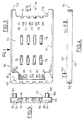
- a connector 64 intended to receive a card C to integrated contact circuit (s) of the "MICRO SIM" type is arranged at inside the case 30.
- the connector 64 essentially consists by a support made of insulating material 66 which delimits in its face upper 68 a housing 70 of complementary shape to that of card C and which is intended to receive at least partially this last of which the lower face 72 has ranges conductors 74 which, when card C is in the inserted position in the housing 70, are in contact with the ends of contact 76 belonging to contact blades 78 of the connector.
- Connector 66 is intended to be mounted with the face lower 67 of the insulation 66 bearing on the upper face 37 of the printed circuit board 36.
- slot 80 which, in the mode of preferred embodiment illustrated in the figures, is arranged in the vicinity from one of the side walls 50 of the connection box 30.
- the insertion slot 80 essentially extends in the inclined portion 82 of the lateral part of the half-shell upper 32 which connects the upper main wall 44 to the fold 60 which extends in the flat portion 84 corresponding to the portion side of reduced thickness of the housing 30.
- the portion 84 'of Part 84 which extends to the right of the slot 80 cut in the inclined part 82, is slightly vertically deformed downward from the general plane of part 84.
- the insertion slot 80 is thus delimited by two upper main edges 86 and 88 and by two edges end 90 and 92.
- the latter comprises, on its lower face 67, four feet 101 in the form of cylindrical pins which are intended, on the one hand, to ensure the positioning and fixing of connector 64 on the plate to printed circuit 36, which for this purpose has holes correspondents 100 through which the feet 101 extend and, secondly, to allow the connector 64 to perform a function spacer between the upper main plates 44 and lower 46 of the housing 30 in order to avoid accidental overwriting housing 30.
- the height of the feet 101 in the form of cylindrical pawns forming a spacer is such that the lower end face 102 of each leg 101 is in contact with the internal face 47 of the lower wall 46 while the upper planar face 68 of the insulating support 66 of connector 64 bears against the face internal facing 45 of the upper wall 44.
- the design of the connector 64 which has a clearance 110 formed in its front edge 112, and its positioning on the circuit board printed 36, relative to slot 80, are such that the ends for connecting contact blades 78 are set back relative to the access zone constituted by the slot 80 avoiding thus any risk of accidental short circuit in case of introduction of a metallic object in the slot 80.
- the housing 30 equipped with the connector 64 thus has a external "silhouette", after introduction of card C, which is identical to that of a conventional case so as to allow its introduction into a corresponding slot of a computer staff.
- notch or extraction groove 114 which is shown in phantom in the figure 6, which extends transversely relative to the housing 30, that is to say parallel to the direction I of introduction or extraction of the map.
- the notch 114 is positioned so as to extend from on either side of the rear transverse edge 98 of the card C and, from preferably facing a connector area 64 does not comprising no metal parts belonging to the blades of contact 78.
- notch 114 it is possible to introduce a small tool dimension in notch 114 to act on the transverse edge rear 98 of card C in order to push it out of its slot 70, i.e. by sliding it from left to right considering figure 6, on the stroke allowed by the length of the notch 114 so that its front transverse edge 99 at least partially out of the housing 30 through the slot 80 so that, at the end of this first extraction phase, the user can grab the card to extract it entirely from the housing 30.
- card C has in the vicinity of its edge transverse before 99 a cutaway 116 which, for some applications, is a way of coding the position of card C in its connector.
Landscapes
- Engineering & Computer Science (AREA)
- Microelectronics & Electronic Packaging (AREA)
- Physics & Mathematics (AREA)
- General Physics & Mathematics (AREA)
- Theoretical Computer Science (AREA)
- Artificial Intelligence (AREA)
- Computer Vision & Pattern Recognition (AREA)
- Coupling Device And Connection With Printed Circuit (AREA)
- Details Of Connecting Devices For Male And Female Coupling (AREA)
Claims (7)
- Elektronisches Anschlußgehäuse (30) mit einer Oberen (32) und einer unteren Wandung (34), die zwischen sich einen Hohlraum (48) abgrenzen, in dem innenliegend ein Stecker (64) ausgebildet ist, der einen Sockel (66) aus isolierenden Material umfasst, zum elektrischen verbinden des Verbindungsgehäuse (30) mit einer Kontaktkarte (C) mit integrierten/integriertem Schaltkreis(en) von der Art, umfassend benachbart der transversalen Vorderkante (99) davon, eine abgeschrägte Kante (116), die für gewisse Anwendungen ein Mittel bildet zur Unverwechselbarkeit der Position der Kontaktkarte (C) in dem Stecker (64), dadurch gekennzeichnet, dass eine obere Hauptwandung (44), auf deren Innenseite (45) einen Höcker (120) umfasst, der, wenn die Kontaktkarte (C) in einer eingeführten Position ist, sich an der abgeschrägten Kante (116) mit geringer Höhe erstreckt, um einen Anschlag zu bilden, der sich in Richtung der abgeschrägten Kante (116) erstreckt, um ein zufälliges Entweichen letzterer zu vermeiden, und daß beim Herausziehen der Kontaktkarte (C) durch eine leichte elastische Verformung des entsprechenden Abschnitts der oberen Hauptwandung (44), der durch den Höcker (120) gebildete Anschlag beim passieren der abgeschrägten Kante (116) und einer oberen Fläche (73) der Kontaktkarte (C) verschwindet.
- Elektronisches Anschlußgehäuse nach Anspruch 1, dadurch gekennzeichnet, dass das isolierende Material eine Aufnahme (70) in einer offenen Oberseite (68) umfasst, begrenzt durch zwei in Einführungsrichtung der Kontaktkarte parallele Ränder (92. 94), und quer, durch zumindest einen Hinterrand (96), die zumindest abschnittsweise die Kontaktkarte (C) aufnimmt, die an einer unteren Hauptfläche (72) Kontaktbereiche (74) umfasst, die mit Kontaktenden (76) von Kontaktelementen (78) wechselwirken, im Boden der Aufnahme (70) des Sockels ausgebildet, wenn die Kontaktkarte (C) in der Anschlußposition vorliegt, in welcher ein transversaler Hinterrand (98) einen Anschlag gegen den transversalen Hinterrand (96) der Aufnahme bildet und dass, die Innenseite (45), gegenüber der oberen Hauptwandung (44) vorliegend, und an welchen der Höcker (120) ausgebildet ist, an die Oberseite (68) des Sockels (66) des Steckers (64) angrenzt.
- Elektronisches Anschlußgehäuse nach einem der vorhergehenden Ansprüche, dadurch gekennzeichnet, dass Ausziehmittel der Kontaktkarte (C) eine Nut (114) in der oberen Hauptwandung (44) umfassen, die sich parallel zu einer Einführungsrichtung (I) der Kontaktkarte (C) erstreckt, um ein Einwirken auf die Kontaktkarte (C) zu ermöglichen, bezüglich der Veranlassung eines Gleitens im inneren der Aufnahme (70) in der dem Herausziehen entsprechenden Richtung.
- Elektronisches Anschlußgehäuse nach Anspruch 3, dadurch gekennzeichnet, dass die Nut (114) sich wenigstens teilweise an dem transversalen Hinterrand (98) der Kontaktkarte (C) erstreckt, wenn letztere sich in der eingeführten Position befindet, um ein Einführen eines Ausziehwerkzeuges zu ermöglichen, das mit dem transversalen Hinterrand der Kontaktkarte wechselwirkt.
- Elektronisches Anschlußgehäuse nach einem der vorhergehenden Ansprüche, dadurch gekennzeichnet, dass dieses einen Schlitz (80) zum Einschieben oder Herausziehen der Kontaktkarte (C) in das Anschlußgehäuse, in einer Richtung (I), die im wesentlichen parallel zu Grundfläche der Kontaktkarte (C) verläuft, umfasst.
- Elektronisches Anschlußgehäuse nach einem der vorhergehenden Ansprüche, dadurch gekennzeichnet, dass in der eingeführten Position, die Kontaktkarte (C) vollständig innenliegend im Anschlußgehäuse (30) angeordnet ist.
- Elektronisches Anschlußgehäuse nach einem der vorhergehenden Ansprüche, dadurch gekennzeichnet, dass in der eingeführten Position in dem Anschlußgehäuse also in einer Anschlußposition bezüglich des Steckers (64) in der Aufnahme (70), die transversale Vorderkante (99) der Kontaktkarte vollständig innerhalb des Anschlußgehäuses (30) liegt, wobei sich ein leichter Rücksprung im Verhältnis zur Hauptkante des Einführschlitzes (80) bildet.
Applications Claiming Priority (3)
| Application Number | Priority Date | Filing Date | Title |
|---|---|---|---|
| FR9604842A FR2747847B1 (fr) | 1996-04-18 | 1996-04-18 | Boitier de raccordement electronique, a un ordinateur individuel, equipe d'un connecteur pour une carte a puce |
| FR9604842 | 1996-04-18 | ||
| EP97923269A EP0846304B1 (de) | 1996-04-18 | 1997-04-07 | Elektronisches verbindungsgehäuse für personalcomputer mit chipkartenverbinder |
Related Parent Applications (1)
| Application Number | Title | Priority Date | Filing Date |
|---|---|---|---|
| EP97923269A Division EP0846304B1 (de) | 1996-04-18 | 1997-04-07 | Elektronisches verbindungsgehäuse für personalcomputer mit chipkartenverbinder |
Publications (3)
| Publication Number | Publication Date |
|---|---|
| EP0860905A2 EP0860905A2 (de) | 1998-08-26 |
| EP0860905A3 EP0860905A3 (de) | 1999-10-06 |
| EP0860905B1 true EP0860905B1 (de) | 2002-07-10 |
Family
ID=9491324
Family Applications (4)
| Application Number | Title | Priority Date | Filing Date |
|---|---|---|---|
| EP98201406A Expired - Lifetime EP0860904B1 (de) | 1996-04-18 | 1997-04-07 | Verbinder für IC-Karte und damit ausgerüstetes Gehäuse |
| EP99201075A Expired - Lifetime EP0942492B1 (de) | 1996-04-18 | 1997-04-07 | Gehäuse zur elektronischen Verbindung an einen Computer ausgerüstet mit einem IC-Karten-Verbinder |
| EP98201407A Expired - Lifetime EP0860905B1 (de) | 1996-04-18 | 1997-04-07 | Gehäuse ausgerüstet mit einem Verbinder für IC-Karte |
| EP97923269A Expired - Lifetime EP0846304B1 (de) | 1996-04-18 | 1997-04-07 | Elektronisches verbindungsgehäuse für personalcomputer mit chipkartenverbinder |
Family Applications Before (2)
| Application Number | Title | Priority Date | Filing Date |
|---|---|---|---|
| EP98201406A Expired - Lifetime EP0860904B1 (de) | 1996-04-18 | 1997-04-07 | Verbinder für IC-Karte und damit ausgerüstetes Gehäuse |
| EP99201075A Expired - Lifetime EP0942492B1 (de) | 1996-04-18 | 1997-04-07 | Gehäuse zur elektronischen Verbindung an einen Computer ausgerüstet mit einem IC-Karten-Verbinder |
Family Applications After (1)
| Application Number | Title | Priority Date | Filing Date |
|---|---|---|---|
| EP97923269A Expired - Lifetime EP0846304B1 (de) | 1996-04-18 | 1997-04-07 | Elektronisches verbindungsgehäuse für personalcomputer mit chipkartenverbinder |
Country Status (9)
| Country | Link |
|---|---|
| US (1) | US6053748A (de) |
| EP (4) | EP0860904B1 (de) |
| JP (4) | JP3313732B2 (de) |
| CN (3) | CN1157680C (de) |
| CA (1) | CA2221890C (de) |
| DE (4) | DE69723461T2 (de) |
| FR (1) | FR2747847B1 (de) |
| TW (4) | TW420785B (de) |
| WO (1) | WO1997039418A1 (de) |
Families Citing this family (36)
| Publication number | Priority date | Publication date | Assignee | Title |
|---|---|---|---|---|
| DE29722142U1 (de) * | 1997-12-16 | 1998-02-12 | Stocko Metallwarenfabriken Henkels & Sohn GmbH & Co, 42327 Wuppertal | Adapter zum Kontaktieren von Chipkarten |
| FR2773275B1 (fr) * | 1997-12-26 | 2000-01-28 | Itt Mfg Enterprises Inc | Connecteur electrique de tres faible epaisseur pour le raccordement d'une carte a memoire electronique |
| DE19846366C2 (de) * | 1998-04-07 | 2000-07-27 | Itt Mfg Enterprises Inc | Steckkarte für elektronische Geräte |
| DE19815549C2 (de) * | 1998-04-07 | 2000-04-27 | Itt Mfg Enterprises Inc | Steckkarte für elektronische Geräte |
| DE29904904U1 (de) * | 1999-03-17 | 1999-06-10 | SCM Microsystems GmbH, 85276 Pfaffenhofen | Chipkartenleser mit Kontaktiereinheit |
| US6599147B1 (en) * | 1999-05-11 | 2003-07-29 | Socket Communications, Inc. | High-density removable expansion module having I/O and second-level-removable expansion memory |
| US6353870B1 (en) * | 1999-05-11 | 2002-03-05 | Socket Communications Inc. | Closed case removable expansion card having interconnect and adapter circuitry for both I/O and removable memory |
| DE19925146C2 (de) * | 1999-06-02 | 2003-01-09 | Itt Mfg Enterprises Inc | Steckkarte für elektronische Geräte |
| GB2352315B (en) * | 1999-07-19 | 2003-12-03 | Nokia Mobile Phones Ltd | Sim card reader |
| JP2001125662A (ja) | 1999-08-18 | 2001-05-11 | Fujitsu Ltd | 情報処理装置用の認証情報入力手段付き拡張装置、認証情報入力ユニット及び情報処理装置 |
| DE19940695B4 (de) | 1999-08-27 | 2008-03-27 | ITT Manufacturing Enterprises, Inc., Wilmington | Elektronisches Mediagerät |
| DE19947162C1 (de) * | 1999-10-01 | 2000-09-28 | Itt Mfg Enterprises Inc | Steckkarte für elektronische Geräte |
| DE10038287A1 (de) * | 2000-08-05 | 2002-02-21 | Itt Mfg Enterprises Inc | Steckkarte für elektronische Geräte |
| US6561851B2 (en) | 2001-04-27 | 2003-05-13 | Sierra Wireless Inc. | Module interface for PC card |
| KR100395896B1 (ko) * | 2001-12-11 | 2003-08-27 | 한국몰렉스 주식회사 | 에스디(sd) 메모리 카드 소켓 |
| TW507950U (en) * | 2001-12-26 | 2002-10-21 | Hon Hai Prec Ind Co Ltd | Electronic card connector |
| US6781831B1 (en) | 2002-02-14 | 2004-08-24 | Mercury Computer Systems, Inc. | Card-cage with integrated control and shaping of flow resistance curve for multiple plenum chambers |
| US6879486B1 (en) | 2002-02-14 | 2005-04-12 | Mercury Computer Systems, Inc. | Central inlet circuit board assembly |
| US7440774B2 (en) | 2002-04-08 | 2008-10-21 | Socket Mobile, Inc. | Wireless enabled memory module |
| US6808396B2 (en) * | 2002-05-24 | 2004-10-26 | Symbol Technologies, Inc. | Connection of a user identity module to a compact card case |
| JP3728669B2 (ja) * | 2002-10-25 | 2005-12-21 | モレックス インコーポレーテッド | カードコネクタ用アダプタ |
| US7240144B2 (en) * | 2004-04-02 | 2007-07-03 | Arm Limited | Arbitration of data transfer requests |
| US6951470B1 (en) * | 2004-10-22 | 2005-10-04 | Huang-Chou Huang | SIM card seat assembly |
| US20060121941A1 (en) * | 2004-12-03 | 2006-06-08 | Shiflett Jamie C | SIM card retaining device |
| DE102006021023A1 (de) * | 2006-04-28 | 2007-10-31 | Würth Elektronik Rot am See GmbH & Co. KG | Baugruppenaufbau |
| TWM319568U (en) * | 2006-11-27 | 2007-09-21 | Ks Terminals Inc | Card connection apparatus and its applications about digital products |
| CN101452537B (zh) * | 2007-11-30 | 2011-11-16 | 深圳富泰宏精密工业有限公司 | 芯片卡固持装置及具有该固持装置的便携式电子装置 |
| US20090172235A1 (en) * | 2007-12-27 | 2009-07-02 | Mei Yan | Megasim card adapter |
| US8325486B2 (en) * | 2009-01-13 | 2012-12-04 | Dy 4 Systems Inc. | Tamper respondent module |
| JP5324234B2 (ja) * | 2009-01-15 | 2013-10-23 | 日本圧着端子製造株式会社 | Icカード |
| US8371866B1 (en) * | 2011-09-09 | 2013-02-12 | Cheng Uei Precision Industry Co., Ltd. | Card connector |
| CN102622056B (zh) * | 2012-03-31 | 2016-05-11 | 惠州Tcl移动通信有限公司 | 一种用户可更换无线通信装置的智能终端 |
| US8651884B1 (en) | 2012-04-10 | 2014-02-18 | Google Inc. | Ejectable memory card tray in a universal serial bus (USB) connector |
| US9604671B2 (en) | 2015-08-13 | 2017-03-28 | Fca Us Llc | Vehicle underbody structure |
| KR101740182B1 (ko) | 2015-12-31 | 2017-05-25 | 몰렉스 엘엘씨 | 카드 소켓, 카드 커넥터 및 이의 제조 방법 |
| FR3115905B1 (fr) * | 2020-10-30 | 2023-03-03 | Banks And Acquirers Int Holding | Connecteur de carte à puce soudable et procédé de montage correspondant. |
Family Cites Families (11)
| Publication number | Priority date | Publication date | Assignee | Title |
|---|---|---|---|---|
| DE2326543C3 (de) * | 1973-05-24 | 1979-08-30 | Siemens Ag, 1000 Berlin Und 8000 Muenchen | Halterung für einen Leitungsstecker |
| FR2607291B1 (fr) * | 1986-11-21 | 1991-04-19 | Flonic Sa | Ensemble de connexion pour cartes a memoire electronique et dispositif de lecture/ecriture en faisant application |
| JPH0492380A (ja) * | 1990-08-06 | 1992-03-25 | Fuji Electric Co Ltd | めすコネクタ |
| FR2667713A1 (fr) * | 1990-10-08 | 1992-04-10 | Cit Alcatel | Lecteur de carte a micro-circuit, a encombrement reduit. |
| US5257414A (en) * | 1990-11-26 | 1993-10-26 | Motorola, Inc. | Apparatus for accepting and retaining a memory card |
| US5503564A (en) * | 1992-10-30 | 1996-04-02 | The Whitaker Corporation | Assembly of an electrical connector and ejector unit for connecting IC cards to printed circuit boards |
| US5476387A (en) * | 1993-06-07 | 1995-12-19 | Methode Electronics Inc. | Memory card frame and cover kit |
| FR2710996B1 (fr) * | 1993-10-06 | 1995-12-01 | Gemplus Card Int | Carte portable multi-applications pour ordinateur personnel. |
| DE29505678U1 (de) * | 1995-04-01 | 1995-06-14 | Stocko Metallwarenfabriken Henkels Und Sohn Gmbh & Co, 42327 Wuppertal | Kontaktiereinheit für kartenförmige Trägerelemente |
| DE29602632U1 (de) * | 1996-02-05 | 1996-05-30 | Neifer, Wolfgang, 85354 Freising | Mobiles Chipkarten-Lesemodul |
| US5752857A (en) * | 1996-05-24 | 1998-05-19 | Itt Corporation | Smart card computer adaptor |
-
1996
- 1996-04-18 FR FR9604842A patent/FR2747847B1/fr not_active Expired - Fee Related
-
1997
- 1997-04-07 CN CNB971903883A patent/CN1157680C/zh not_active Expired - Fee Related
- 1997-04-07 DE DE69723461T patent/DE69723461T2/de not_active Expired - Fee Related
- 1997-04-07 CA CA002221890A patent/CA2221890C/en not_active Expired - Fee Related
- 1997-04-07 WO PCT/IB1997/000595 patent/WO1997039418A1/fr not_active Ceased
- 1997-04-07 DE DE69713871T patent/DE69713871T2/de not_active Expired - Fee Related
- 1997-04-07 JP JP53691197A patent/JP3313732B2/ja not_active Expired - Fee Related
- 1997-04-07 EP EP98201406A patent/EP0860904B1/de not_active Expired - Lifetime
- 1997-04-07 DE DE69706958T patent/DE69706958T2/de not_active Expired - Fee Related
- 1997-04-07 EP EP99201075A patent/EP0942492B1/de not_active Expired - Lifetime
- 1997-04-07 EP EP98201407A patent/EP0860905B1/de not_active Expired - Lifetime
- 1997-04-07 DE DE69713564T patent/DE69713564T2/de not_active Expired - Fee Related
- 1997-04-07 EP EP97923269A patent/EP0846304B1/de not_active Expired - Lifetime
- 1997-04-15 TW TW087106991A patent/TW420785B/zh not_active IP Right Cessation
- 1997-04-15 TW TW088106284A patent/TW420787B/zh not_active IP Right Cessation
- 1997-04-15 TW TW086104823A patent/TW416039B/zh not_active IP Right Cessation
- 1997-04-15 TW TW087106992A patent/TW420786B/zh not_active IP Right Cessation
- 1997-04-17 US US08/837,421 patent/US6053748A/en not_active Expired - Fee Related
-
1998
- 1998-05-22 CN CN98108935A patent/CN1117417C/zh not_active Expired - Fee Related
- 1998-06-18 JP JP17141898A patent/JP3974260B2/ja not_active Expired - Fee Related
- 1998-06-18 JP JP17141798A patent/JP3974259B2/ja not_active Expired - Fee Related
-
1999
- 1999-04-27 JP JP11920899A patent/JP3902350B2/ja not_active Expired - Fee Related
- 1999-09-27 CN CN99120718.1A patent/CN1118908C/zh not_active Expired - Fee Related
Also Published As
Similar Documents
| Publication | Publication Date | Title |
|---|---|---|
| EP0860905B1 (de) | Gehäuse ausgerüstet mit einem Verbinder für IC-Karte | |
| FR3017253B1 (fr) | Connecteur electrique | |
| EP0756242B1 (de) | Anordnung zur Verbindung einer Chipkarte mit Kontakten in einer Lese- und Schreibvorrichtung und zugehörige Kappe | |
| EP0549460B1 (de) | Modularer elektrischer Steckverbinder | |
| EP0549461B1 (de) | Modularer elektrischer Steckverbinder | |
| FR2821988A1 (fr) | Connecteur electrique pour cartes a memoire electronique a grande capacite de stockage | |
| FR2742561A1 (fr) | Connecteur electrique pour une carte a circuit(s) integre(s) a contact | |
| EP0738429B1 (de) | Elektrischer verbinder für eine elektronische speicherkarte mit elektrischen isolationverdrängungsverbindern | |
| EP0549462A1 (de) | Elektrischer Steckverbinder zum Aufnehmen einer Leiterplatte | |
| FR2793353A1 (fr) | Connecteur electrique monobloc pour le raccordement d'une carte a circuit(s) integre(s) | |
| FR2488059A1 (fr) | Connecteur electrique destine a etre dispose a l'extremite d'un cable electrique plat a plusieurs conducteurs | |
| CA2075753C (fr) | Joint d'etancheite, notamment d'etancheite electromagnetique | |
| FR2684242A1 (fr) | Assemblage de connecteur electrique comportant un element de verrouillage des bornes. | |
| FR2803110A1 (fr) | Connecteur pour carte a microcircuit et procede de montage d'une telle carte dans ce connecteur | |
| FR2800520A1 (fr) | Perfectionnement aux dispositifs de connexion pour circuit souple | |
| EP0401121B1 (de) | Verbindungszusammenbau für gedruckte Schaltungskarten | |
| CA1186388A (fr) | Module electronique enfichable dans un connecteur de bus | |
| FR2668627A1 (fr) | Cadre de contact pour lecteur de carte a puce. | |
| EP0738983B1 (de) | Elektrischer Verbinder für eine Kontaktkarte mit integrierten Schaltungen | |
| EP0720761B1 (de) | Kontakt-chipkartenhalter | |
| FR2759183A1 (fr) | Connecteur electrique pour le raccordement d'une carte a circuit(s) integre(s) et boitier equipe d'un tel connecteur | |
| EP0720760B1 (de) | Chipkartenhalter | |
| FR2759184A1 (fr) | Connecteur pour le raccordement d'une carte a circuit(s) integre(s) et boitier equipe d'un tel connecteur | |
| EP0560648B1 (de) | Polygonal Steckverbinder, insbesondere viereckig mit einem isolierenden Zentralkörper | |
| FR3106466A1 (fr) | Tiroir électronique et ensemble électronique associé |
Legal Events
| Date | Code | Title | Description |
|---|---|---|---|
| PUAI | Public reference made under article 153(3) epc to a published international application that has entered the european phase |
Free format text: ORIGINAL CODE: 0009012 |
|
| AC | Divisional application: reference to earlier application |
Ref document number: 846304 Country of ref document: EP |
|
| AK | Designated contracting states |
Kind code of ref document: A2 Designated state(s): DE FI FR GB IT SE |
|
| PUAL | Search report despatched |
Free format text: ORIGINAL CODE: 0009013 |
|
| AK | Designated contracting states |
Kind code of ref document: A3 Designated state(s): DE FI FR GB IT SE |
|
| RIC1 | Information provided on ipc code assigned before grant |
Free format text: 6H 01R 13/514 A, 6H 01R 23/70 B, 6G 06K 7/00 B, 6H 05K 5/02 B |
|
| 17P | Request for examination filed |
Effective date: 20000229 |
|
| 17Q | First examination report despatched |
Effective date: 20001208 |
|
| RTI1 | Title (correction) |
Free format text: HOUSING EQUIPPED WITH A CONNECTOR FOR INTEGRATED CIRCUIT CARD |
|
| GRAG | Despatch of communication of intention to grant |
Free format text: ORIGINAL CODE: EPIDOS AGRA |
|
| RTI1 | Title (correction) |
Free format text: HOUSING EQUIPPED WITH A CONNECTOR FOR INTEGRATED CIRCUIT CARD |
|
| GRAG | Despatch of communication of intention to grant |
Free format text: ORIGINAL CODE: EPIDOS AGRA |
|
| GRAH | Despatch of communication of intention to grant a patent |
Free format text: ORIGINAL CODE: EPIDOS IGRA |
|
| GRAH | Despatch of communication of intention to grant a patent |
Free format text: ORIGINAL CODE: EPIDOS IGRA |
|
| GRAA | (expected) grant |
Free format text: ORIGINAL CODE: 0009210 |
|
| AC | Divisional application: reference to earlier application |
Ref document number: 846304 Country of ref document: EP |
|
| AK | Designated contracting states |
Kind code of ref document: B1 Designated state(s): DE FI FR GB IT SE |
|
| REG | Reference to a national code |
Ref country code: GB Ref legal event code: FG4D Free format text: NOT ENGLISH |
|
| RIC1 | Information provided on ipc code assigned before grant |
Free format text: 7H 01R 13/514 A, 7H 01R 12/18 B, 7G 06K 7/00 B, 7H 05K 5/02 B |
|
| REF | Corresponds to: |
Ref document number: 69713871 Country of ref document: DE Date of ref document: 20020814 |
|
| GBT | Gb: translation of ep patent filed (gb section 77(6)(a)/1977) |
Effective date: 20020814 |
|
| PLBE | No opposition filed within time limit |
Free format text: ORIGINAL CODE: 0009261 |
|
| STAA | Information on the status of an ep patent application or granted ep patent |
Free format text: STATUS: NO OPPOSITION FILED WITHIN TIME LIMIT |
|
| 26N | No opposition filed |
Effective date: 20030411 |
|
| REG | Reference to a national code |
Ref country code: GB Ref legal event code: 732E |
|
| PGFP | Annual fee paid to national office [announced via postgrant information from national office to epo] |
Ref country code: DE Payment date: 20080602 Year of fee payment: 12 |
|
| REG | Reference to a national code |
Ref country code: FR Ref legal event code: TP |
|
| PGFP | Annual fee paid to national office [announced via postgrant information from national office to epo] |
Ref country code: IT Payment date: 20080428 Year of fee payment: 12 Ref country code: FI Payment date: 20080430 Year of fee payment: 12 |
|
| PGFP | Annual fee paid to national office [announced via postgrant information from national office to epo] |
Ref country code: SE Payment date: 20080429 Year of fee payment: 12 |
|
| PGFP | Annual fee paid to national office [announced via postgrant information from national office to epo] |
Ref country code: FR Payment date: 20080417 Year of fee payment: 12 |
|
| PGFP | Annual fee paid to national office [announced via postgrant information from national office to epo] |
Ref country code: GB Payment date: 20080429 Year of fee payment: 12 |
|
| EUG | Se: european patent has lapsed | ||
| GBPC | Gb: european patent ceased through non-payment of renewal fee |
Effective date: 20090407 |
|
| REG | Reference to a national code |
Ref country code: FR Ref legal event code: ST Effective date: 20091231 |
|
| PG25 | Lapsed in a contracting state [announced via postgrant information from national office to epo] |
Ref country code: FI Free format text: LAPSE BECAUSE OF NON-PAYMENT OF DUE FEES Effective date: 20090407 Ref country code: DE Free format text: LAPSE BECAUSE OF NON-PAYMENT OF DUE FEES Effective date: 20091103 |
|
| PG25 | Lapsed in a contracting state [announced via postgrant information from national office to epo] |
Ref country code: GB Free format text: LAPSE BECAUSE OF NON-PAYMENT OF DUE FEES Effective date: 20090407 Ref country code: FR Free format text: LAPSE BECAUSE OF NON-PAYMENT OF DUE FEES Effective date: 20091222 |
|
| PG25 | Lapsed in a contracting state [announced via postgrant information from national office to epo] |
Ref country code: IT Free format text: LAPSE BECAUSE OF NON-PAYMENT OF DUE FEES Effective date: 20090407 |
|
| PG25 | Lapsed in a contracting state [announced via postgrant information from national office to epo] |
Ref country code: SE Free format text: LAPSE BECAUSE OF NON-PAYMENT OF DUE FEES Effective date: 20090408 |