EP0860948B1 - Pufferverstärker für Bussteuerung - Google Patents
Pufferverstärker für Bussteuerung Download PDFInfo
- Publication number
- EP0860948B1 EP0860948B1 EP98410015A EP98410015A EP0860948B1 EP 0860948 B1 EP0860948 B1 EP 0860948B1 EP 98410015 A EP98410015 A EP 98410015A EP 98410015 A EP98410015 A EP 98410015A EP 0860948 B1 EP0860948 B1 EP 0860948B1
- Authority
- EP
- European Patent Office
- Prior art keywords
- transistor
- buffer amplifier
- channel mos
- circuit
- mos transistor
- Prior art date
- Legal status (The legal status is an assumption and is not a legal conclusion. Google has not performed a legal analysis and makes no representation as to the accuracy of the status listed.)
- Expired - Lifetime
Links
- 239000000758 substrate Substances 0.000 claims description 11
- 238000005516 engineering process Methods 0.000 claims description 8
- 239000003990 capacitor Substances 0.000 description 4
- 239000004065 semiconductor Substances 0.000 description 2
- 230000000295 complement effect Effects 0.000 description 1
- 230000000694 effects Effects 0.000 description 1
- 235000021183 entrée Nutrition 0.000 description 1
- 238000004519 manufacturing process Methods 0.000 description 1
- 125000006850 spacer group Chemical group 0.000 description 1
- 230000007704 transition Effects 0.000 description 1
- 238000011144 upstream manufacturing Methods 0.000 description 1
Images


Classifications
-
- H—ELECTRICITY
- H03—ELECTRONIC CIRCUITRY
- H03K—PULSE TECHNIQUE
- H03K19/00—Logic circuits, i.e. having at least two inputs acting on one output; Inverting circuits
- H03K19/01—Modifications for accelerating switching
- H03K19/017—Modifications for accelerating switching in field-effect transistor circuits
- H03K19/01707—Modifications for accelerating switching in field-effect transistor circuits in asynchronous circuits
- H03K19/01721—Modifications for accelerating switching in field-effect transistor circuits in asynchronous circuits by means of a pull-up or down element
-
- H—ELECTRICITY
- H03—ELECTRONIC CIRCUITRY
- H03K—PULSE TECHNIQUE
- H03K19/00—Logic circuits, i.e. having at least two inputs acting on one output; Inverting circuits
- H03K19/0175—Coupling arrangements; Interface arrangements
- H03K19/0185—Coupling arrangements; Interface arrangements using field effect transistors only
- H03K19/018507—Interface arrangements
Definitions
- the present invention relates to the field of circuits integrated and more particularly the production of buffer amplifiers in MOS type integrated circuits.
- buffer amplifiers whose role is to adapt the impedance of the logic signal to the bus to be controlled.
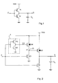
- Figure 1 shows the most common type of buffer amplifier used in MOS technology.
- This buffer amplifier consists of a simple inverter comprising two complementary MOS transistors, P channel and N channel respectively, P1 and N1, connected in series between a high supply line Vdd and ground.
- the gates of the transistors P1 and N1 are connected together to an input terminal E, and the common drain of the transistors P1 and N1 is connected to an output terminal S.
- a capacitor C L the equivalent load of the line or bus connected to terminal S.
- a second solution is to split the line connected to terminal S and use a buffer amplifier to each line fraction. This solution obviously leads an increase in the overall size of the circuit.
- An object of the present invention is to provide a high switching speed buffer amplifier made of MOS technology.
- Another object of the present invention is to provide a buffer amplifier with low input capacity.
- Another object of the present invention is to provide a buffer amplifier capable of controlling a line capable of to be capacitive.
- Another object of the present invention is to provide an amplifier-buffer circuit of optimal surface.
- a bus control buffer amplifier comprising a terminal input and an output terminal connected to the output line, the output terminal being associated with a first MOS transistor with low level N channel and to a second MOS transistor at high level N channel, the first channel MOS transistor N being directly controlled by an input signal.
- the second MOS transistor is N-channel, and its gate is controlled by a third MOS transistor at low level N channel directly controlled by signal input, and by a fourth N-channel MOS transistor high level, which is controlled by the inverted input signal; and the fourth N-channel MOS transistor includes a junction very abrupt drain-substrate.
- the substrate of the fourth N-channel MOS transistor is floating.
- the buffer amplifier is made in submicronic technology.
- the substrate of the second N-channel MOS transistor is floating.
- the second N-channel MOS transistor has the same dimensions as the first N-channel MOS transistor.
- the fourth transistor is defined so that the surface of the fourth transistor is three times smaller than that of second transistor.
- the fourth transistor is defined so that the length channel of the fourth transistor is six times that of the third transistor.
- FIG. 2 represents a buffer amplifier according to the present invention.
- This buffer amplifier is connected between an input terminal E and an output terminal S connected to a load of capacity C L.
- the output terminal S is connected to the drain of an N-channel MOS transistor N1 and to the source of an N-channel MOS transistor N2.
- the source of transistor N1 is connected to ground, and the drain of transistor N2 is connected to a power source Vdd.
- N-channel MOS transistors N3 and N4 are connected in series between ground and the high supply voltage Vdd.
- the connection point 10 of the transistors N3 and N4 is connected to the gate of the transistor N2.
- the gates of transistors N1 and N3 are directly connected to input terminal E.
- the gate of transistor N4 is connected to the input terminal E via an inverter 11.
- the inverter 11 comprises, for example, in a conventional manner, a P-channel MOS transistor P5 and an N-channel MOS transistor N5 in series between the power source Vdd and the ground.
- transistors N1 and N3 are blocked and transistor N4 becomes conducting, which turns transistor N2 on and tends to set output terminal S at high level, that is to say that one begins to charge the capacitor C L.
- the circuit according to the present invention seems have a disadvantage rather than an advantage over prior art circuit because the high output voltage is limited, a disadvantage which is particularly serious when supply voltages are low and today is the tendency of integrated circuits to use supply voltages high increasingly low, for example of the order of 3 V.
- the present invention not only plans to use the circuit described above but also to realize this circuit and in particular the transistor N4 in a particular technology.
- Figure 3 schematically shows a sectional view of a conventional MOS transistor formed in a P-type semiconductor substrate 21 above a buried layer 22 of N + type.
- This transistor comprises a heavily N-type source region 23 and a source extension region 24 as well as a heavily N-type drain region 25 and a drain extension region 26.
- a gate 28 is formed above a gate insulating layer 29 and is surrounded by spacers 30.
- the present invention uses transistors for the circuit, and in particular for the transistor N4 of the MOS transistors made in submicronic technology (in which the length grids is less than 0.5 ⁇ m).
- a specific characteristic of such technology is that the drain and source are heavily doped and shallow, i.e. the junction between the drain or the source and the substrate is very abrupt.
- this phenomenon is more marked if transistor N4 has a floating substrate.
- FIG. 5 illustrates the relationship between the rise time of the output signal (tr S ) and the rise time of the input signal (tr E ) for the buffer amplifier circuit according to the present invention.
- the rise time of the output signal increases slowly for short rise times of the input signal (less than 2 ns), then increases suddenly. This shows that the overvoltage effect on node 10 occurs well for very fast growing input signals.
- FIG. 6 illustrates the relationship between the rise time of the output signal (tr S ) and the capacitive load for the circuit according to the present invention (curve 61) and for a conventional circuit (curve 62).
- the rise time of the output signal varies linearly with the capacitance C L.
- the slope is lower in the case of the circuit according to the present invention. It can be seen that for high capacities (around 10 pF for example) the value of the rise time is reduced by around 15%. This shows that the device according to the invention provides a significant improvement in the switching speed for a line with a high capacitive load.
- the inventors have also observed that consumption power of a circuit according to the present invention was no different from that of a classic circuit.
- the present invention provides a circuit with low input capacity because, unlike the conventional circuit, the P-channel transistor does not intervene directly to charge the capacitor C L , and therefore no longer needs to be large.
- a circuit according to the present invention will have an input capacity reduced by about 50% compared to that of the conventional circuit.
- the present invention also provides a circuit for minimal surface because, even if the number of circuit components of the present invention is high compared to that of a circuit conventional, these components can be small.
- the maximum advantages of the present invention are obtained in the case where the output transistors N1 and N2 are N-channel MOS transistors. Note, however, that even when these transistors are NPN bipolar transistors, the invention retains advantages over the state of the art. Indeed, even if the NPN transistors are essentially fast switches, the invention provides the advantage of providing an increase in the output voltage excursion. Indeed, thanks to the overvoltage brought by the transistor N4 on the terminal control (base) of transistor N2, we prevent the voltage high available on the output terminal S is one lower base-emitter voltage drop (Vbe) at supply voltage high (Vdd).
Landscapes
- Engineering & Computer Science (AREA)
- Computer Hardware Design (AREA)
- Physics & Mathematics (AREA)
- Computing Systems (AREA)
- General Engineering & Computer Science (AREA)
- Mathematical Physics (AREA)
- Logic Circuits (AREA)
- Amplifiers (AREA)
Claims (8)
- Ein Bussteuerpufferverstärker mit einem Eingangsanschluss (E) und einem Ausgangsanschluss (S), verbunden mit der Ausgangsleitung, wobei der Ausgangsanschluss mit einem ersten "Pull"-Transistor (N1) und einem zweiten "Pull-up"-Transistor (N2) verbunden ist, wobei der erste Transistor direkt durch ein Eingangssignal geregelt wird, wobei Folgendes vorgesehen ist:das Gate des zweiten Transistors (N2) wird durch einen dritten direkt durch das Eingangssignal gesteuerten "Pull-down" N-Kanal-MOS-Transistor (N3) und durch einen vierten "Pull-up" N-Kanal-MOS-Transsitor (N4), der durch das invertierte Eingangssignal gesteuert wird; undferner dadurch gekennzeichnet, dass der vierte N-Kanal-MOS-Transistor (N4) eine sehr abrupte Drain-Substrat-Grenzschicht (junction) aufweist.
- Der Pufferverstärker nach Anspruch 1, dadurch gekennzeichnet, dass die ersten (N1) und zweiten (N2) Transistoren N-Kanal-MOS-Transistoren sind.
- Der Pufferverstärker nach Anspruch 1, dadurch gekennzeichnet, dass das Substrat des vierten N-Kanal-MOS-Transistors (N4) ein schwimmendes Substrat ist.
- Der Pufferverstärker nach Anspruch 1, dadurch gekennzeichnet, dass die Implementierung in Submikrontechnologie erfolgt.
- Der Pufferverstärker nach Anspruch 2, dadurch gekennzeichnet, dass das Substrat des zweiten N-Kanal-MOS-Transistors ein schwimmendes Substrat ist.
- Der Pufferverstärker nach Anspruch 2, dadurch gekennzeichnet, dass der zweite N-Kanal-MOS-Transistor die gleichen Dimensionen besitzt wie der erste N-Kanal-MOS-Transistor.
- Der Pufferverstärker nach Anspruch 2, dadurch gekennzeichnet, dass der vierte Transistor derart definiert ist, dass das Oberflächengebiet oder die Oberfläche des vierten Transistors dreimal kleiner ist als die des zweiten Transistors.
- Der Pufferverstärker nach Anspruch 2, dadurch gekennzeichnet, dass der vierte Transistor derart definiert ist, dass die Kanallänge des vierten Transistors gleich dem sechsfachen des dritten Transistors ist.
Applications Claiming Priority (2)
| Application Number | Priority Date | Filing Date | Title |
|---|---|---|---|
| FR9702459A FR2760151B1 (fr) | 1997-02-25 | 1997-02-25 | Amplificateur-tampon de commande de bus |
| FR9702459 | 1997-02-25 |
Publications (2)
| Publication Number | Publication Date |
|---|---|
| EP0860948A1 EP0860948A1 (de) | 1998-08-26 |
| EP0860948B1 true EP0860948B1 (de) | 2004-08-18 |
Family
ID=9504326
Family Applications (1)
| Application Number | Title | Priority Date | Filing Date |
|---|---|---|---|
| EP98410015A Expired - Lifetime EP0860948B1 (de) | 1997-02-25 | 1998-02-24 | Pufferverstärker für Bussteuerung |
Country Status (5)
| Country | Link |
|---|---|
| US (1) | US6144257A (de) |
| EP (1) | EP0860948B1 (de) |
| JP (1) | JP3179059B2 (de) |
| DE (1) | DE69825646T2 (de) |
| FR (1) | FR2760151B1 (de) |
Families Citing this family (8)
| Publication number | Priority date | Publication date | Assignee | Title |
|---|---|---|---|---|
| JP3539947B2 (ja) * | 2002-06-20 | 2004-07-07 | 沖電気工業株式会社 | パワー検出回路付リミティングアンプ |
| US7777996B2 (en) * | 2005-06-30 | 2010-08-17 | Lsi Corporation | Circuit protection system |
| JP4787554B2 (ja) * | 2005-07-01 | 2011-10-05 | パナソニック株式会社 | 入出力回路装置 |
| US8144848B2 (en) * | 2007-06-27 | 2012-03-27 | At&T Intellectual Property I, Lp | System and method for telephone directory advertising |
| US7825732B2 (en) * | 2007-10-24 | 2010-11-02 | Infineon Technologies Ag | Compensation for amplifiers driving a capacitive load |
| US8085956B2 (en) * | 2007-12-14 | 2011-12-27 | Knowles Electronics, Llc | Filter circuit for an electret microphone |
| US8575975B1 (en) * | 2009-01-28 | 2013-11-05 | Cirrus Logic, Inc. | Stepped voltage drive for driving capacitive loads |
| US8400211B2 (en) | 2010-10-15 | 2013-03-19 | Taiwan Semiconductor Manufacturing Company, Ltd. | Integrated circuits with reduced voltage across gate dielectric and operating methods thereof |
Family Cites Families (9)
| Publication number | Priority date | Publication date | Assignee | Title |
|---|---|---|---|---|
| US3806738A (en) * | 1972-12-29 | 1974-04-23 | Ibm | Field effect transistor push-pull driver |
| JPS5198938A (de) * | 1975-02-26 | 1976-08-31 | ||
| US4071783A (en) * | 1976-11-29 | 1978-01-31 | International Business Machines Corporation | Enhancement/depletion mode field effect transistor driver |
| US4199695A (en) * | 1978-03-03 | 1980-04-22 | International Business Machines Corporation | Avoidance of hot electron operation of voltage stressed bootstrap drivers |
| US4714840A (en) * | 1982-12-30 | 1987-12-22 | Thomson Components - Mostek Corporation | MOS transistor circuits having matched channel width and length dimensions |
| US4542310A (en) * | 1983-06-29 | 1985-09-17 | International Business Machines Corporation | CMOS bootstrapped pull up circuit |
| US5191244A (en) * | 1991-09-16 | 1993-03-02 | Advanced Micro Devices, Inc. | N-channel pull-up transistor with reduced body effect |
| JPH05167427A (ja) * | 1991-12-13 | 1993-07-02 | Toshiba Corp | レベルシフト回路 |
| US5422591A (en) * | 1994-01-03 | 1995-06-06 | Sgs-Thomson Microelectronics, Inc. | Output driver circuit with body bias control for multiple power supply operation |
-
1997
- 1997-02-25 FR FR9702459A patent/FR2760151B1/fr not_active Expired - Fee Related
-
1998
- 1998-02-24 DE DE69825646T patent/DE69825646T2/de not_active Expired - Fee Related
- 1998-02-24 JP JP05738398A patent/JP3179059B2/ja not_active Expired - Fee Related
- 1998-02-24 US US09/028,408 patent/US6144257A/en not_active Expired - Lifetime
- 1998-02-24 EP EP98410015A patent/EP0860948B1/de not_active Expired - Lifetime
Also Published As
| Publication number | Publication date |
|---|---|
| FR2760151A1 (fr) | 1998-08-28 |
| EP0860948A1 (de) | 1998-08-26 |
| JP3179059B2 (ja) | 2001-06-25 |
| DE69825646D1 (de) | 2004-09-23 |
| JPH10256897A (ja) | 1998-09-25 |
| FR2760151B1 (fr) | 1999-05-14 |
| DE69825646T2 (de) | 2005-08-18 |
| US6144257A (en) | 2000-11-07 |
Similar Documents
| Publication | Publication Date | Title |
|---|---|---|
| EP0388329B1 (de) | Steuerschaltung für einen MOS-Leistungstransistor mit induktiver Last | |
| EP0357528B1 (de) | MOS-Transistor und Anwendung bei einer Freilaufdiode | |
| EP0594834B1 (de) | In Standard-CMOS-Technologie realisierte, zwischen einer Logikschaltung mit niedriger Versorgungsspannung und einer Ausgangsstufe mit hoher Versorgungsspannung, liegende Schaltung | |
| FR2536607A1 (fr) | Circuit d'interface | |
| EP0328465B1 (de) | Gate-Steuerschaltung eines MOS-Leistungstransistors im Schaltbetrieb | |
| EP0432058B1 (de) | Dynamische Isolierschaltung für integrierte Schaltungen | |
| FR2634311A1 (fr) | Circuit tampon de sortie de donnees pour une memoire d'octets | |
| FR2693327A1 (fr) | Circuit de commutation de haute tension. | |
| EP0860948B1 (de) | Pufferverstärker für Bussteuerung | |
| EP0678802A1 (de) | Schaltungsanordnung zur Spannungsbegrenzung mit Hysteresiskomparator | |
| EP0359680A1 (de) | Integrierbare, aktive Diode | |
| FR2970611A1 (fr) | Étage de sortie forme dans et sur un substrat de type soi | |
| EP0881682B1 (de) | Hochspannungsschutzanordnung für einen integrierten MOS-Leistungstransistor | |
| FR2886783A1 (fr) | Pompe a charge bi-directionnelle a haut rendement | |
| FR2665775A1 (fr) | Circuit de commande en technologie mos. | |
| EP0865671A1 (de) | Normal leitender dual-thyristor | |
| FR2911450A1 (fr) | Circuit tampon a haute vitesse | |
| WO2002052364A1 (fr) | Regulateur de tension a gain statique en boucle ouverte reduit | |
| FR3134487A1 (fr) | Dispositif de copie d'un courant | |
| EP0109106A1 (de) | Schaltung zur Signalpegelumsetzung zwischen gesättigter und ungesättigter Logik | |
| EP3651363A1 (de) | Adiabatische logische zelle | |
| EP0553020B1 (de) | TTL-CMOS-Ausgangsstufe für integrierte Schaltungen | |
| EP0700162B1 (de) | Logische Schaltung mit Differenzstufen | |
| FR3103333A1 (fr) | Dispositif pour générer un courant | |
| FR2762727A1 (fr) | Circuit integre avec etage de sortie haute tension |
Legal Events
| Date | Code | Title | Description |
|---|---|---|---|
| PUAI | Public reference made under article 153(3) epc to a published international application that has entered the european phase |
Free format text: ORIGINAL CODE: 0009012 |
|
| AK | Designated contracting states |
Kind code of ref document: A1 Designated state(s): DE FR GB IT |
|
| RAP3 | Party data changed (applicant data changed or rights of an application transferred) |
Owner name: STMICROELECTRONICS S.A. |
|
| 17P | Request for examination filed |
Effective date: 19990128 |
|
| AKX | Designation fees paid |
Free format text: DE FR GB IT |
|
| RBV | Designated contracting states (corrected) |
Designated state(s): DE FR GB IT |
|
| RAP1 | Party data changed (applicant data changed or rights of an application transferred) |
Owner name: STMICROELECTRONICS S.A. |
|
| GRAP | Despatch of communication of intention to grant a patent |
Free format text: ORIGINAL CODE: EPIDOSNIGR1 |
|
| GRAS | Grant fee paid |
Free format text: ORIGINAL CODE: EPIDOSNIGR3 |
|
| GRAA | (expected) grant |
Free format text: ORIGINAL CODE: 0009210 |
|
| AK | Designated contracting states |
Kind code of ref document: B1 Designated state(s): DE FR GB IT |
|
| PG25 | Lapsed in a contracting state [announced via postgrant information from national office to epo] |
Ref country code: IT Free format text: LAPSE BECAUSE OF FAILURE TO SUBMIT A TRANSLATION OF THE DESCRIPTION OR TO PAY THE FEE WITHIN THE PRE;WARNING: LAPSES OF ITALIAN PATENTS WITH EFFECTIVE DATE BEFORE 2007 MAY HAVE OCCURRED AT ANY TIME BEFORE 2007. THE CORRECT EFFECTIVE DATE MAY BE DIFFERENT FROM THE ONE RECORDED.SCRIBED TIME-LIMIT Effective date: 20040818 |
|
| REG | Reference to a national code |
Ref country code: GB Ref legal event code: FG4D Free format text: NOT ENGLISH |
|
| REF | Corresponds to: |
Ref document number: 69825646 Country of ref document: DE Date of ref document: 20040923 Kind code of ref document: P |
|
| GBT | Gb: translation of ep patent filed (gb section 77(6)(a)/1977) |
Effective date: 20040922 |
|
| PLBE | No opposition filed within time limit |
Free format text: ORIGINAL CODE: 0009261 |
|
| STAA | Information on the status of an ep patent application or granted ep patent |
Free format text: STATUS: NO OPPOSITION FILED WITHIN TIME LIMIT |
|
| 26N | No opposition filed |
Effective date: 20050519 |
|
| PGFP | Annual fee paid to national office [announced via postgrant information from national office to epo] |
Ref country code: GB Payment date: 20080129 Year of fee payment: 11 |
|
| PGFP | Annual fee paid to national office [announced via postgrant information from national office to epo] |
Ref country code: FR Payment date: 20080228 Year of fee payment: 11 |
|
| PGFP | Annual fee paid to national office [announced via postgrant information from national office to epo] |
Ref country code: DE Payment date: 20090227 Year of fee payment: 12 |
|
| GBPC | Gb: european patent ceased through non-payment of renewal fee |
Effective date: 20090224 |
|
| REG | Reference to a national code |
Ref country code: FR Ref legal event code: ST Effective date: 20091030 |
|
| PG25 | Lapsed in a contracting state [announced via postgrant information from national office to epo] |
Ref country code: GB Free format text: LAPSE BECAUSE OF NON-PAYMENT OF DUE FEES Effective date: 20090224 Ref country code: FR Free format text: LAPSE BECAUSE OF NON-PAYMENT OF DUE FEES Effective date: 20090302 |
|
| PG25 | Lapsed in a contracting state [announced via postgrant information from national office to epo] |
Ref country code: DE Free format text: LAPSE BECAUSE OF NON-PAYMENT OF DUE FEES Effective date: 20100901 |