EP0861640A2 - Mikroelektronischer Positionssensor - Google Patents
Mikroelektronischer Positionssensor Download PDFInfo
- Publication number
- EP0861640A2 EP0861640A2 EP98610004A EP98610004A EP0861640A2 EP 0861640 A2 EP0861640 A2 EP 0861640A2 EP 98610004 A EP98610004 A EP 98610004A EP 98610004 A EP98610004 A EP 98610004A EP 0861640 A2 EP0861640 A2 EP 0861640A2
- Authority
- EP
- European Patent Office
- Prior art keywords
- magnetic field
- position sensor
- sensor according
- assembly
- sensitive elements
- Prior art date
- Legal status (The legal status is an assumption and is not a legal conclusion. Google has not performed a legal analysis and makes no representation as to the accuracy of the status listed.)
- Granted
Links
- 235000014676 Phragmites communis Nutrition 0.000 claims description 32
- 239000004020 conductor Substances 0.000 claims description 24
- 210000002105 tongue Anatomy 0.000 claims description 19
- 230000005355 Hall effect Effects 0.000 claims description 3
- 230000003068 static effect Effects 0.000 description 10
- 230000002093 peripheral effect Effects 0.000 description 7
- 238000004377 microelectronic Methods 0.000 description 6
- 230000006870 function Effects 0.000 description 5
- XUIMIQQOPSSXEZ-UHFFFAOYSA-N Silicon Chemical compound [Si] XUIMIQQOPSSXEZ-UHFFFAOYSA-N 0.000 description 3
- 239000000463 material Substances 0.000 description 3
- 229910052710 silicon Inorganic materials 0.000 description 3
- 239000010703 silicon Substances 0.000 description 3
- 230000003213 activating effect Effects 0.000 description 2
- 239000012141 concentrate Substances 0.000 description 2
- 238000010276 construction Methods 0.000 description 2
- 230000000712 assembly Effects 0.000 description 1
- 238000000429 assembly Methods 0.000 description 1
- 238000010923 batch production Methods 0.000 description 1
- 239000003575 carbonaceous material Substances 0.000 description 1
- 239000000428 dust Substances 0.000 description 1
- 238000004070 electrodeposition Methods 0.000 description 1
- 238000005516 engineering process Methods 0.000 description 1
- 230000004907 flux Effects 0.000 description 1
- 230000010354 integration Effects 0.000 description 1
- 238000001459 lithography Methods 0.000 description 1
- 239000000696 magnetic material Substances 0.000 description 1
- 238000013507 mapping Methods 0.000 description 1
- 239000011159 matrix material Substances 0.000 description 1
- 238000000034 method Methods 0.000 description 1
- 238000012986 modification Methods 0.000 description 1
- 230000004048 modification Effects 0.000 description 1
- 238000000206 photolithography Methods 0.000 description 1
- 238000007747 plating Methods 0.000 description 1
- 239000007787 solid Substances 0.000 description 1
- 239000010409 thin film Substances 0.000 description 1
Images

Classifications
-
- H—ELECTRICITY
- H01—ELECTRIC ELEMENTS
- H01H—ELECTRIC SWITCHES; RELAYS; SELECTORS; EMERGENCY PROTECTIVE DEVICES
- H01H36/00—Switches actuated by change of magnetic field or of electric field, e.g. by change of relative position of magnet and switch, by shielding
- H01H36/0006—Permanent magnet actuating reed switches
- H01H36/006—Permanent magnet actuating reed switches comprising a plurality of reed switches, e.g. selectors or joystick-operated
-
- H—ELECTRICITY
- H01—ELECTRIC ELEMENTS
- H01H—ELECTRIC SWITCHES; RELAYS; SELECTORS; EMERGENCY PROTECTIVE DEVICES
- H01H1/00—Contacts
- H01H1/0036—Switches making use of microelectromechanical systems [MEMS]
-
- H—ELECTRICITY
- H01—ELECTRIC ELEMENTS
- H01H—ELECTRIC SWITCHES; RELAYS; SELECTORS; EMERGENCY PROTECTIVE DEVICES
- H01H36/00—Switches actuated by change of magnetic field or of electric field, e.g. by change of relative position of magnet and switch, by shielding
- H01H2036/0093—Micromechanical switches actuated by a change of the magnetic field
-
- H—ELECTRICITY
- H01—ELECTRIC ELEMENTS
- H01H—ELECTRIC SWITCHES; RELAYS; SELECTORS; EMERGENCY PROTECTIVE DEVICES
- H01H2300/00—Orthogonal indexing scheme relating to electric switches, relays, selectors or emergency protective devices covered by H01H
- H01H2300/004—Application hearing aid
Definitions
- the invention relates to a microelectric position sensor for use in microelectronic equipment.
- the microelectric position sensor according to the invention is of the type including an assembly of magnetic field sensitive elements such as micro miniature reed switches or Hall effect elements, and means creating a magnetic field such as a permanent magnet for selectively influencing and activating the magnetic field sensitive elements.
- the magnetic field sensitive elements each have a switching function, and they thus form an assembly of switches which are operated by the magnet.
- the assembly of switches can be connected to an assembly of e.g. thin film resistors, whereby e.g. a potentiometer with discrete positions can be made.
- the assembly of switches can control the performance and functions of the digital circuit.
- a microelectric position sensor of the invention will find its main applications in microelectronic equipment such as hearing instruments where it can be used for controlling the gain or the output volume and other settings of the hearing instrument.
- Hearing instruments have been subject to a continuing miniaturisation, and in particular the electronic circuits have been miniaturised.
- Modern analogue hearing instruments typically include up to a hundred electronic components or elements, whereas modern digital hearing instruments of the all-in-the-ear type may include integrated circuits with hundreds of thousands of electronic elements.
- a microelectric position sensor according to the invention is suitable for such use in analogue as well as in digital hearing instruments.
- Traditional electro-mechanical resistive track potentiometers or trimmers convert a manually set angular or linear position to a corresponding resistive divider ratio according to a mapping function, which, in principle, is continuous.
- the operating principle is based on an electrically conductive wiper, which is moved manually along or around a distributed track of resistive material, e.g. a carbon based material.
- Low resistance electrical contacts are provided at both ends of the track and also at the wiper, and such potentiometers provide a resistive division of a voltage applied at the ends of the track by translation of a linear or angular position of the movable part of the potentiometer.
- Switches Traditional electro-mechanical slide or rotational switches rely on a mechanical wiper with an electrically conductive tip or edge which opens or closes the electrical contact between two or more terminals of the switch. The opening and closing function of switches may then be used for selecting, enabling or disabling different parts of electric circuitry connected to the switch.
- US Patent No. 5,592,079 discloses such a known microelectric position sensor, however without any focusing of the magnetic field.
- US Patent No. 4,258,346 discloses an arrangement including an assembly of magnetically actuated relays mounted adjacent a magnetic shield having an assembly of holes therein corresponding to the location of the relays.
- the shield prevents magnetic flux which is applied to one of the relays from being spilled over and inadvertently actuating a nearby relay.
- the magnet creating the magnetic field activating and deactivating the magnetic field sensitive elements includes focusing means focusing the magnetic field to a region including substantially only one of the magnetic field sensitive elements.
- a microelectronic position sensor having such a focusing arrangement can be made substantially smaller and more compact than any of the known devices, and, as a very important advantage, it can include a much higher number of individual magnetic field sensitive elements, thereby achieving the desired higher resolution.
- the magnetic field sensitive elements are micro reed switches, but Hall effect elements may also be used with minor modifications, which are obvious to the skilled person.
- the gain control in hearing instruments usually has a rotary knob, and for this use the assembly of magnetic field sensitive elements are provided in a circular assembly.
- the magnetic field sensitive elements can be arranged in a linear assembly.
- An arrangement of the magnetic field sensitive elements in a two-dimensional assembly or matrix is also possible. This embodiment can be applied in high resolution proximity or touch sensitive surfaces and can be used in joy sticks and other pointing devices.
- FIGS 1, 2A and 2B illustrate a microelectric position sensor of the rotary type.
- the sensor has a base 10 of silicon or other suitable material carrying a circular disc-shaped static part 11 also of silicon in solid connection with the base 10.
- the static part 11 carries an assembly of micro reed contactors or switches 13.
- a cover 12 of an inverted cup shape is fixed over the static part 11 and rests with its edge on the base 10 and thus covers and protects the reed contactors 13 e.g. against dust.
- the base 10, the static part 11 and the cover 12 together form, together with the reed contactors, a static construction.
- the reed contactors 13 can be manufactured in a number of ways, but for this application a preferred contactor is described in the article A New Reed Micro-contactor Fabricated by Multilevel UV-lithography and Electrodeposition, Intermediate report M 2 S 2 1994, pp. 4-5, ASULAB SA., CSEM.
- the microcontactors are thus fabricated using photo lithography techniques adapted from microelectronics combined with advanced plating technology. Important features of these micro reed contactors are that they are very small, typically smaller than 100 ⁇ m * 100 ⁇ m, the excellent device properties and the potential possibility of batch production of monolithic assemblies of micro reed contactors.
- the cover 12 carries a bar magnet 14 of permanently magnetised material.
- the bar magnet 14 rests near its two ends on magnetic focusing devices which, in the shown embodiment are shaped like tongues 15 and 16 consisting of magnetically conductive material.
- the tongues 15 and 16 have end portions 15a and 16a distant from the bar magnet 14.
- the focusing tongues 15 and 16 concentrate the magnetic field created by the bar magnet 14 in a region about a selected one of the micro reed contactors 13.
- Centrally each micro reed contactor 13 is connected to a central part 17 of magnetically and electrically conductive material common to all the micro reed contactors, and peripherally each micro reed contactor has its own individual peripheral part 18 also of magnetically and electrically conductive material.
- the end portion 16a of the focusing tongue 16 is situated above the central part 17 common to all the reed contactors, whereas the end portion 15a of the focusing tongue 15 is situated above the peripheral part 18 of one of the reed contactors 13 and is sized to concentrate the magnetic field at the peripheral part of a selected one of the reed contactors.
- a magnetic circuit is thus formed by the bar magnet 14, the focusing tongues 15 and 16, a selected one of the reed contactors 13 including the peripheral part 18 thereof and the central part 17, thereby causing the selected micro reed contactor to be activated and to close the electrical path between the common central part 17 and the individual peripheral part 18 corresponding to the selected micro reed contactor.
- Electrical terminals (not shown) are connected in known manner to the common central part 17 and to each of the individual peripheral parts 18.
- the bar magnet 14 and the focusing tongues 15 and 16 are connected to a (not shown) finger wheel and can be rotated about the central axis 19 relatively to the static construction formed by the base 10, the static part 11 and the cover 12, thereby displacing the end portion 15a of the focusing tongue 15 across the circular assembly of micro reed contactors 13, whereby the micro reed contactors will be activated individually, and electric contact will be created between the common central part 17 and the peripheral part 18 of the selected one of the micro reed contactors 13.
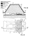
- FIGS 3A and 3B illustrate another embodiment of the invention on a larger scale.
- a static part 51 of silicon carries an assembly of micro reed contactors 53.
- each of the micro reed contactors 53 has a comb of tongues 60 which, at their roots 61, are connected to a common magnetic and electric conductor 57.
- the tongues 60 When activated by a magnetic field, the tongues 60 will bend and touch respective ones of electrical and magnetic conductors 62 on the static part 51.
- An electric and magnetic terminal 58 is situated at the opposite ends of the electrical and magnetic conductors 62, with a small electrically insulating gap 63 between the conductors 62 and the terminal 58.
- a movable part 52 is movably arranged above the micro reed contactors 53 on the static part 51.
- the movable part 52 carries a bar magnet 54 of permanent magnetic material.
- the opposed ends of the magnet 54 are connected to magnetic focusing tongues 55 and 56 of magnetically conductive material.
- the tongues 55 and 56 have the same function as the tongues 15 and 16, namely to focus the magnetic field from the magnet 54 on the common magnetic and electric conductor 57 and on an individual one of the electric and magnetic terminals 58, so that only one micro reed contactor 53 with its comb of tongues 60 will be activated.
- the electrical and magnetic conductors 62 are covered by an insulating layer 64, and electrical conductors 65 are provided on top of the insulating layer 64.
- the illustrated embodiment includes six electrical conductors 65 and six tongues 60 in the comb of each of the micro reed contactors 53.
- the six conductors 65 are connected to (not shown) output terminals of the microelectric position sensor.
- the electrical conductors 65 are connected to individual ones of the underlying electric and magnetic conductors 62. Electric contact is established at the contact points 67 through the insulating layer 64.
- Each micro reed contactor 53 has its individual combination of electrical conductors 65 connected to the electrical and magnetic conductors 62.
- the output terminal connected to the common electric conductor 57 will typically be connected to a reference potential such as ground potential representing logic '0' (zero), and the electrical conductors 65 will carry a binary code representing the position of the movable part 52.
- the output of the microelectric position sensor will be a digital code of the physical position of the gain control, which can be used by the digital circuits of the hearing instrument to set the gain correspondingly.
Landscapes
- Measurement Of Length, Angles, Or The Like Using Electric Or Magnetic Means (AREA)
- Transmission And Conversion Of Sensor Element Output (AREA)
Applications Claiming Priority (2)
| Application Number | Priority Date | Filing Date | Title |
|---|---|---|---|
| DK199700227A DK173778B1 (da) | 1997-02-28 | 1997-02-28 | En mikroelektrisk positionssensor |
| DK22797 | 1997-02-28 |
Publications (3)
| Publication Number | Publication Date |
|---|---|
| EP0861640A2 true EP0861640A2 (de) | 1998-09-02 |
| EP0861640A3 EP0861640A3 (de) | 1998-09-16 |
| EP0861640B1 EP0861640B1 (de) | 2003-04-16 |
Family
ID=8091164
Family Applications (1)
| Application Number | Title | Priority Date | Filing Date |
|---|---|---|---|
| EP98610004A Expired - Lifetime EP0861640B1 (de) | 1997-02-28 | 1998-02-27 | Mikroelektronischer Positionssensor |
Country Status (5)
| Country | Link |
|---|---|
| US (1) | US6012021A (de) |
| EP (1) | EP0861640B1 (de) |
| JP (1) | JPH116707A (de) |
| DE (1) | DE69813352T2 (de) |
| DK (2) | DK173778B1 (de) |
Cited By (1)
| Publication number | Priority date | Publication date | Assignee | Title |
|---|---|---|---|---|
| CN102867699A (zh) * | 2011-07-08 | 2013-01-09 | 富士康(昆山)电脑接插件有限公司 | 微开关及其制造方法 |
Families Citing this family (6)
| Publication number | Priority date | Publication date | Assignee | Title |
|---|---|---|---|---|
| US6593731B1 (en) * | 1999-07-08 | 2003-07-15 | California Institute Of Technology | Displacement transducer utilizing miniaturized magnet and hall junction |
| US6859542B2 (en) | 2001-05-31 | 2005-02-22 | Sonion Lyngby A/S | Method of providing a hydrophobic layer and a condenser microphone having such a layer |
| US6850849B1 (en) | 2001-06-20 | 2005-02-01 | Curtis Roys | Fluid flow monitor and control system |
| US6823270B1 (en) | 2001-06-20 | 2004-11-23 | Curtis Roys | Fluid flow monitoring system |
| US7072482B2 (en) | 2002-09-06 | 2006-07-04 | Sonion Nederland B.V. | Microphone with improved sound inlet port |
| US8712084B2 (en) | 2010-12-07 | 2014-04-29 | Sonion Nederland Bv | Motor assembly |
Family Cites Families (6)
| Publication number | Priority date | Publication date | Assignee | Title |
|---|---|---|---|---|
| US3139600A (en) * | 1960-12-12 | 1964-06-30 | Sylvania Electric Prod | Variable voltage generator |
| JPS6026430Y2 (ja) * | 1980-11-19 | 1985-08-09 | 株式会社 千野製作所 | 切換器 |
| GB2128027B (en) * | 1982-10-01 | 1985-11-06 | Electronic Components Ltd | Gearbox indicator switch |
| JPH0241544Y2 (de) * | 1985-08-13 | 1990-11-06 | ||
| GB8620079D0 (en) * | 1986-08-18 | 1986-10-01 | Walsh A B | Switch |
| EP0699295B1 (de) * | 1992-09-03 | 1997-04-09 | Microtronic A/S | Mikroelektronischer positionssensor |
-
1997
- 1997-02-28 DK DK199700227A patent/DK173778B1/da not_active IP Right Cessation
-
1998
- 1998-02-27 EP EP98610004A patent/EP0861640B1/de not_active Expired - Lifetime
- 1998-02-27 US US09/034,615 patent/US6012021A/en not_active Expired - Lifetime
- 1998-02-27 DE DE69813352T patent/DE69813352T2/de not_active Expired - Lifetime
- 1998-02-27 DK DK98610004T patent/DK0861640T3/da active
- 1998-03-02 JP JP10092154A patent/JPH116707A/ja active Pending
Cited By (2)
| Publication number | Priority date | Publication date | Assignee | Title |
|---|---|---|---|---|
| CN102867699A (zh) * | 2011-07-08 | 2013-01-09 | 富士康(昆山)电脑接插件有限公司 | 微开关及其制造方法 |
| CN102867699B (zh) * | 2011-07-08 | 2016-03-02 | 富士康(昆山)电脑接插件有限公司 | 微开关及其制造方法 |
Also Published As
| Publication number | Publication date |
|---|---|
| DK0861640T3 (da) | 2003-07-21 |
| DE69813352T2 (de) | 2004-04-08 |
| US6012021A (en) | 2000-01-04 |
| EP0861640A3 (de) | 1998-09-16 |
| EP0861640B1 (de) | 2003-04-16 |
| DE69813352D1 (de) | 2003-05-22 |
| DK173778B1 (da) | 2001-10-08 |
| JPH116707A (ja) | 1999-01-12 |
| DK22797A (da) | 1998-08-29 |
Similar Documents
| Publication | Publication Date | Title |
|---|---|---|
| US5829987A (en) | Electromechanical connection device | |
| US5867082A (en) | Switch with magnetically-coupled armature | |
| US4489297A (en) | Magnetic switch | |
| EP1154451A1 (de) | Schalter mit magnetisch gekoppeltem Anker | |
| EP1028446A2 (de) | Kombinierter Druckknopf- und Drehschalter | |
| GB2052871A (en) | Switch with wetted contacts | |
| EP0861640B1 (de) | Mikroelektronischer Positionssensor | |
| WO2013022756A1 (en) | Pushbutton switch | |
| US6351232B1 (en) | Electrical appliance with parameterable function at reduced cost | |
| EP0286388B1 (de) | Elektrische Steuervorrichtung | |
| US2794861A (en) | Combination telephone switch and dial | |
| EP0500127A2 (de) | Drucktaster-Schiebeschalter | |
| US3814886A (en) | Miniature electrical reversing switch mounted on trigger operated switch for hand-held tools | |
| US5120912A (en) | Membrane switch with series resistor | |
| US3665127A (en) | Thumbwheel switch with floatingly positioned actuator | |
| US4525607A (en) | Simplified electric switch construction | |
| US3346708A (en) | Rotary switch with roller detent apparatus directly biasing contact structure into open and closed positions | |
| US5075516A (en) | Miniature single in-line package electrical switch | |
| US3736396A (en) | Minimum friction contactors | |
| US5153391A (en) | Binary coded decimal (BCD) switch assembly with integral chip | |
| US3198895A (en) | Rotary electrical switch with recessed contacts and sealing means | |
| WO1993007633A1 (en) | Joystick | |
| US5144278A (en) | Variable impedance device and circuit for sensing adjustment thereof | |
| GB2223831A (en) | Joystick controller with reed switches | |
| US4680433A (en) | Contact assembly for a switch |
Legal Events
| Date | Code | Title | Description |
|---|---|---|---|
| PUAI | Public reference made under article 153(3) epc to a published international application that has entered the european phase |
Free format text: ORIGINAL CODE: 0009012 |
|
| PUAL | Search report despatched |
Free format text: ORIGINAL CODE: 0009013 |
|
| AK | Designated contracting states |
Kind code of ref document: A2 Designated state(s): CH DE DK GB LI NL |
|
| AX | Request for extension of the european patent |
Free format text: AL;LT;LV;MK;RO;SI |
|
| AK | Designated contracting states |
Kind code of ref document: A3 Designated state(s): AT BE CH DE DK ES FI FR GB GR IE IT LI LU MC NL PT SE |
|
| AX | Request for extension of the european patent |
Free format text: AL;LT;LV;MK;RO;SI |
|
| 17P | Request for examination filed |
Effective date: 19990225 |
|
| AKX | Designation fees paid |
Free format text: AT BE CH DE DK LI |
|
| RBV | Designated contracting states (corrected) |
Designated state(s): AT BE CH DE DK LI |
|
| RBV | Designated contracting states (corrected) |
Designated state(s): CH DE DK GB LI NL |
|
| 17Q | First examination report despatched |
Effective date: 20010412 |
|
| GRAG | Despatch of communication of intention to grant |
Free format text: ORIGINAL CODE: EPIDOS AGRA |
|
| GRAG | Despatch of communication of intention to grant |
Free format text: ORIGINAL CODE: EPIDOS AGRA |
|
| GRAH | Despatch of communication of intention to grant a patent |
Free format text: ORIGINAL CODE: EPIDOS IGRA |
|
| RAP1 | Party data changed (applicant data changed or rights of an application transferred) |
Owner name: SONIONMEMS A/S |
|
| GRAH | Despatch of communication of intention to grant a patent |
Free format text: ORIGINAL CODE: EPIDOS IGRA |
|
| GRAA | (expected) grant |
Free format text: ORIGINAL CODE: 0009210 |
|
| AK | Designated contracting states |
Designated state(s): CH DE DK GB LI NL |
|
| REG | Reference to a national code |
Ref country code: GB Ref legal event code: FG4D |
|
| REG | Reference to a national code |
Ref country code: CH Ref legal event code: EP |
|
| REG | Reference to a national code |
Ref country code: CH Ref legal event code: NV Representative=s name: KIRKER & CIE SA |
|
| REF | Corresponds to: |
Ref document number: 69813352 Country of ref document: DE Date of ref document: 20030522 Kind code of ref document: P |
|
| REG | Reference to a national code |
Ref country code: DK Ref legal event code: T3 |
|
| PLBE | No opposition filed within time limit |
Free format text: ORIGINAL CODE: 0009261 |
|
| STAA | Information on the status of an ep patent application or granted ep patent |
Free format text: STATUS: NO OPPOSITION FILED WITHIN TIME LIMIT |
|
| 26N | No opposition filed |
Effective date: 20040119 |
|
| PGFP | Annual fee paid to national office [announced via postgrant information from national office to epo] |
Ref country code: DK Payment date: 20100211 Year of fee payment: 13 Ref country code: CH Payment date: 20100215 Year of fee payment: 13 |
|
| PGFP | Annual fee paid to national office [announced via postgrant information from national office to epo] |
Ref country code: GB Payment date: 20100224 Year of fee payment: 13 Ref country code: DE Payment date: 20100312 Year of fee payment: 13 |
|
| PGFP | Annual fee paid to national office [announced via postgrant information from national office to epo] |
Ref country code: NL Payment date: 20100209 Year of fee payment: 13 |
|
| REG | Reference to a national code |
Ref country code: NL Ref legal event code: V1 Effective date: 20110901 |
|
| REG | Reference to a national code |
Ref country code: CH Ref legal event code: PL |
|
| REG | Reference to a national code |
Ref country code: DK Ref legal event code: EBP |
|
| GBPC | Gb: european patent ceased through non-payment of renewal fee |
Effective date: 20110227 |
|
| PG25 | Lapsed in a contracting state [announced via postgrant information from national office to epo] |
Ref country code: CH Free format text: LAPSE BECAUSE OF NON-PAYMENT OF DUE FEES Effective date: 20110228 Ref country code: LI Free format text: LAPSE BECAUSE OF NON-PAYMENT OF DUE FEES Effective date: 20110228 |
|
| PG25 | Lapsed in a contracting state [announced via postgrant information from national office to epo] |
Ref country code: NL Free format text: LAPSE BECAUSE OF NON-PAYMENT OF DUE FEES Effective date: 20110901 |
|
| REG | Reference to a national code |
Ref country code: DE Ref legal event code: R119 Ref document number: 69813352 Country of ref document: DE Effective date: 20110901 |
|
| PG25 | Lapsed in a contracting state [announced via postgrant information from national office to epo] |
Ref country code: GB Free format text: LAPSE BECAUSE OF NON-PAYMENT OF DUE FEES Effective date: 20110227 |
|
| PG25 | Lapsed in a contracting state [announced via postgrant information from national office to epo] |
Ref country code: DE Free format text: LAPSE BECAUSE OF NON-PAYMENT OF DUE FEES Effective date: 20110901 |