EP0864957A2 - Circuit à tension de sortie constante - Google Patents
Circuit à tension de sortie constante Download PDFInfo
- Publication number
- EP0864957A2 EP0864957A2 EP98301089A EP98301089A EP0864957A2 EP 0864957 A2 EP0864957 A2 EP 0864957A2 EP 98301089 A EP98301089 A EP 98301089A EP 98301089 A EP98301089 A EP 98301089A EP 0864957 A2 EP0864957 A2 EP 0864957A2
- Authority
- EP
- European Patent Office
- Prior art keywords
- constant voltage
- emitter
- bipolar transistor
- electric potential
- resistor
- Prior art date
- Legal status (The legal status is an assumption and is not a legal conclusion. Google has not performed a legal analysis and makes no representation as to the accuracy of the status listed.)
- Withdrawn
Links
Images

Classifications
-
- G—PHYSICS
- G05—CONTROLLING; REGULATING
- G05F—SYSTEMS FOR REGULATING ELECTRIC OR MAGNETIC VARIABLES
- G05F3/00—Non-retroactive systems for regulating electric variables by using an uncontrolled element, or an uncontrolled combination of elements, such element or such combination having self-regulating properties
- G05F3/02—Regulating voltage or current
- G05F3/08—Regulating voltage or current wherein the variable is DC
- G05F3/10—Regulating voltage or current wherein the variable is DC using uncontrolled devices with non-linear characteristics
- G05F3/16—Regulating voltage or current wherein the variable is DC using uncontrolled devices with non-linear characteristics being semiconductor devices
- G05F3/20—Regulating voltage or current wherein the variable is DC using uncontrolled devices with non-linear characteristics being semiconductor devices using diode- transistor combinations
- G05F3/30—Regulators using the difference between the base-emitter voltages of two bipolar transistors operating at different current densities
Definitions
- the invention relates to a constant voltage output circuit and, more particularly, to a constant voltage output circuit which can lighten a restriction in a manufacturing process and can obtain a wide voltage set range.
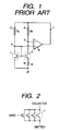
- Fig. 1 is a diagram showing an example of a conventional constant voltage output circuit.
- reference numeral 1 denotes a bipolar transistor (hereinafter, abbreviated to BJT); 2 indicates a BJT whose size is larger than the BJT 1.
- the size of BJT 2 is generally just integer times as large as the size of BJT 1.
- Reference numerals 3 and 4 denote resistors having a same resistance value R 0 . Terminals 5 and 6 of the resistors 3 and 4 are connected to collector terminals of the BJT 1 and BJT 2, respectively. The other terminals of the resistors 3 and 4 are mutually connected and become a common terminal 7.
- Reference numeral 8 denotes a resistor of a resistance value R 1 connecting an emitter of the BJT 2 and the ground and 9 indicates an operational amplifier (hereinafter, referred to as an ope-amplifier) in which a (+) input terminal (non-inverting input terminal) is connected to the terminal 5, a (-) input terminal (inverting input terminal) is connected to the terminal 6, and an output is connected to the common terminal 7.
- An emitter of the BJT 1 is directly connected to the ground. Bases of the BJTs 1 and 2 are mutually connected to the terminal 5.
- Fig. 2 shows a constructional example of the BJT 2.
- Collectors of four BJTs 1' of the same size as that of the BJT 1 are mutually connected, their bases are mutually connected, and their emitters are mutually connected, thereby setting the size of BJT 2 to be just four times as large as that of BJT 1.
- a current flowing the resistor 3, namely, a collector current of the BJT 1 is labeled as I 0 . Since electric potentials of the terminals 5 and 6 are equal due to the operation of the operational amplifier 9, a current flowing in the resistor 4, namely, the collector current of the BJT 2 is also equal to I 0 .
- V BG V BE1 + I 0 R 0
- a predetermined output voltage is derived from the terminal 7.
- a voltage level can be accurately set.
- An output of the ope-amplifier which is used in the above example is also a collector current source of the BJT and it is necessary to use an ope-amplifier having a high current supplying ability. There is inevitably a problem such that the size of ope-amplifier has to be enlarged.
- V BG can be changed by selecting the set potentials of V BE1 .
- a range where normal current-voltage characteristics of the bipolar transistor can be held is a range of about 0.5 to 0.7 V as V BE1
- the constant voltage output in only a range of about 1.1 to 1.3 V can be also set. In other words, there is a problem such that a selection width of the constant voltage output value is narrow.
- Still another object of the invention is to provide a constant voltage output circuit which can easily accomplish a miniaturization and a small area that is occupied by the circuit.
- Another object of the invention is to provide a constant voltage output circuit which can obtain a wide range of a constant voltage output that can be set.
- Another object of the invention is to provide a constant voltage output circuit which can perform a constant voltage output of high performance by a simple construction and can be also applied to a CMOS process.
- Another object of the invention is to provide a constant voltage output circuit comprising: first and second bipolar transistors whose bases are mutually connected; a first resistor for connecting an emitter of the first bipolar transistor to a constant voltage source; second and third resistors which are serially connected and connect an emitter of the second bipolar transistor to the constant voltage source; and means for deciding a common base electric potential of the first and second bipolar transistors so that an electric potential of the emitter of the first bipolar transistor and an electric potential of a connecting portion of the second and third resistors are equalized.
- Another object of the invention is to provide a constant voltage output circuit having first and second bipolar transistors each having a base, an emitter, and a collector, wherein the bases of the first and second bipolar transistors are electrically mutually connected, the emitter of the first bipolar transistor is connected to a line which is set to a predetermined electric potential through a first resistor, the emitter of the second bipolar transistor is connected to the line that was set to the predetermined potential through second and third resistors which are serially connected, an operational amplifier is arranged so that an electric potential between the emitter of the first bipolar transistor and the first resistor and an electric potential between the second and third resistors regarding the second bipolar transistors are inputted, and an output terminal of the operational amplifier and the bases of the first and second bipolar transistors are connected.
- a constant voltage output circuit comprising: first and second BJTs whose bases are mutually connected; a first resistor for connecting an emitter of the first BJT to a constant voltage source (for example, a ground or a ground potential or the like); and second and third resistors which are serially connected and connect an emitter of the second BJT to the constant voltage source, wherein a common base electric potential of the first and second BJTs is determined so that an electric potential of the emitter of the first BJT and an electric potential of a node between the second and third resistors are equalized.
- collectors of the BJTs can be connected to a common electric potential, a manufacturing process which is used in the invention can be simplified than the conventional one. Since it is sufficient to merely control the base potential in the constant voltage output, a scale of an operational amplifier (ope-amplifier) or the like can be reduced in the invention. Further, by controlling the base potential by a resistance division of an output of the operational amplifier or the like, a degree of freedom of selection of a set value of the constant voltage output can be remarkably widened.
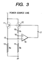
- Fig. 3 is a diagram for explaining a preferred example of a circuit of the invention.
- reference numeral 11 denotes a BJT and 12 indicates a BJT whose size is larger than that of the BJT 11.
- the size of BJT 12 is set to be just integer times as large as the size of BJT 11.
- Reference numeral 13 denotes a resistor having a resistance value R 0 .
- An emitter 15 of the BJT 11 is connected to one terminal of the resistor 13 and the other terminal of the resistor 13 is connected to the ground.
- Reference numeral 14 denotes a resistor having the same resistance value R 0 as that of the resistor 13.
- One input terminal of the resistor 14 is connected to the ground and another terminal 16 is connected to one terminal of a resistor 18 having another resistance value R 1 .
- the other terminal of the resistor 18 is connected to an emitter of the BJT 12.
- Reference numeral 19 denotes an operational amplifier in which a (+) input terminal is connected to the terminal 16 and a (-) input terminal is connected to the terminal 15 and an output terminal 17 is commonly connected to bases of the BJTs 11 and 12.
- a constant voltage output which does not depend on a power source voltage and a temperature is generated at the terminal 17 and its value is determined by the sum of a voltage drop amount of the resistor R 0 and a difference between the base-emitter potentials of the BJTs, so that the constant voltage output is equal to the same value of about 1.2V as that in the foregoing example.
- the construction such that the collector terminals are independent as in the foregoing circuit is unnecessary. Therefore, for example, it is also possible to use a BJT fixed to a semiconductor substrate. In other words, the semiconductor substrate can be also used as a collector region. Further, even if the formation of the BJT is not a purpose, the invention can be accomplished. For example, even in the CMOS process, the circuit of the invention can be constructed by using a parasitic bipolar transistor in which a P well is used as a base and an n-type source drain is used as an emitter and an n-type common substrate is used as a collector. According to the invention as mentioned above, the constant voltage output can be realized by a simpler manufacturing process or by taking into consideration of a design layout of a semiconductor device even if any special process is not particularly executed.
- Fig. 3 it is a base current of the BJT that is driven by the output of the ope-amplifier serving as a constant voltage output.
- a current supply amount of the constant voltage output in the invention is extremely small. Therefore, a scale of the ope-amplifier which is used in the constant voltage output circuit can be sufficiently reduced.
- Fig. 4 is a diagram showing the second embodiment of the invention.
- reference numeral 20 denotes a common terminal of the bases of the BJTs 11 and 12; 21 a resistor having a resistance value R 2 for connecting the terminals 17 and 20; and 22 a resistor having a resistance value R 3 for connecting the terminal 17 and the ground level.
- R 2 a resistor having a resistance value for connecting the terminals 17 and 20
- R 3 a resistor having a resistance value for connecting the terminal 17 and the ground level.
- the same component elements as those in Fig. 3 are designated by the same reference numerals and their descriptions are omitted.
- a current flowing in the terminal 20 is so smaller than the current flowing in the resistors 21 and 22 that it can be sufficiently ignored.
- a voltage of the terminal 20 has a voltage value obtained by dividing the voltage of the terminal 17 by the resistances R 2 and R 3 .
- the voltage of the terminal 20 is a constant voltage of about 1.2V shown in the first embodiment of the invention, so that a voltage value of (R 2 + R 3 )/R 3 times as high as the voltage at the terminal 20 appears at the terminal 17.
- R 2 and R 3 By properly selecting R 2 and R 3 , a value of 1.2V or higher can be freely set as a constant voltage output value.
- the constant voltage is determined by the base potential of the BJT, by multiplying such a value by a gain of a resistance ratio, freedom of selecting of the constant voltage output value can be made greater.
- NPN transistors as BJTs (bipolar transistors)
- the invention can be also applied to a constant voltage output circuit constructed by using PNP transistors.
- the restriction with respect to the manufacturing process to which the constant voltage output circuit can be applied can be remarkably lightened (on the contrary, the process is not made complicated).
- the constant voltage output circuit of the invention can be applied. Since a restriction with regard to the current supplying ability of the ope-amplifier which is used in the constant voltage output circuit is also remarkably lightened, the scale of the ope-amplifier or the like can be reduced. Further, although a range which can be set as a constant voltage value is about 1.1 to 1.3 V hitherto, according to the invention, the constant voltage setting range can be extremely widened. It will be obviously understood that the constant voltage output can be stably performed.
Landscapes
- Engineering & Computer Science (AREA)
- Microelectronics & Electronic Packaging (AREA)
- Physics & Mathematics (AREA)
- Power Engineering (AREA)
- Nonlinear Science (AREA)
- Electromagnetism (AREA)
- General Physics & Mathematics (AREA)
- Radar, Positioning & Navigation (AREA)
- Automation & Control Theory (AREA)
- Control Of Electrical Variables (AREA)
Applications Claiming Priority (2)
| Application Number | Priority Date | Filing Date | Title |
|---|---|---|---|
| JP9030082A JPH10228326A (ja) | 1997-02-14 | 1997-02-14 | 定電圧出力回路 |
| JP30082/97 | 1997-02-14 |
Publications (2)
| Publication Number | Publication Date |
|---|---|
| EP0864957A2 true EP0864957A2 (fr) | 1998-09-16 |
| EP0864957A3 EP0864957A3 (fr) | 1999-03-31 |
Family
ID=12293884
Family Applications (1)
| Application Number | Title | Priority Date | Filing Date |
|---|---|---|---|
| EP98301089A Withdrawn EP0864957A3 (fr) | 1997-02-14 | 1998-02-13 | Circuit à tension de sortie constante |
Country Status (3)
| Country | Link |
|---|---|
| US (1) | US6020731A (fr) |
| EP (1) | EP0864957A3 (fr) |
| JP (1) | JPH10228326A (fr) |
Families Citing this family (2)
| Publication number | Priority date | Publication date | Assignee | Title |
|---|---|---|---|---|
| US6707286B1 (en) * | 2003-02-24 | 2004-03-16 | Ami Semiconductor, Inc. | Low voltage enhanced output impedance current mirror |
| US7772920B1 (en) * | 2009-05-29 | 2010-08-10 | Linear Technology Corporation | Low thermal hysteresis bandgap voltage reference |
Family Cites Families (11)
| Publication number | Priority date | Publication date | Assignee | Title |
|---|---|---|---|---|
| US4714872A (en) * | 1986-07-10 | 1987-12-22 | Tektronix, Inc. | Voltage reference for transistor constant-current source |
| US4924113A (en) * | 1988-07-18 | 1990-05-08 | Harris Semiconductor Patents, Inc. | Transistor base current compensation circuitry |
| US4945260A (en) * | 1989-04-17 | 1990-07-31 | Advanced Micro Devices, Inc. | Temperature and supply compensated ECL bandgap reference voltage generator |
| JPH03185506A (ja) * | 1989-12-14 | 1991-08-13 | Toyota Motor Corp | 安定化定電圧回路 |
| US5319303A (en) * | 1992-02-12 | 1994-06-07 | Sony/Tektronix Corporation | Current source circuit |
| US5291122A (en) * | 1992-06-11 | 1994-03-01 | Analog Devices, Inc. | Bandgap voltage reference circuit and method with low TCR resistor in parallel with high TCR and in series with low TCR portions of tail resistor |
| JP3293699B2 (ja) * | 1993-09-03 | 2002-06-17 | キヤノン株式会社 | 増幅装置 |
| FR2711258A1 (fr) * | 1993-10-13 | 1995-04-21 | Philips Composants | Circuit générateur de tension stabilisée du type bandgap. |
| DE69325027T2 (de) * | 1993-12-02 | 1999-09-16 | Co.Ri.M.Me. Consorzio Per La Ricerca Sulla Microelettronica Nel Mezzogiorno, Catania | Spannungsreferenz mit linearem negativem Temperaturkoeffizienten |
| DE19521663A1 (de) * | 1995-06-14 | 1996-12-19 | Philips Patentverwaltung | Integrierter Schaltkreis mit Spannungsregelschaltung |
| DE19530737A1 (de) * | 1995-08-22 | 1997-02-27 | Philips Patentverwaltung | Schaltungsanordnung zum Liefern eines konstanten Stromes |
-
1997
- 1997-02-14 JP JP9030082A patent/JPH10228326A/ja active Pending
-
1998
- 1998-02-12 US US09/022,411 patent/US6020731A/en not_active Expired - Fee Related
- 1998-02-13 EP EP98301089A patent/EP0864957A3/fr not_active Withdrawn
Also Published As
| Publication number | Publication date |
|---|---|
| US6020731A (en) | 2000-02-01 |
| JPH10228326A (ja) | 1998-08-25 |
| EP0864957A3 (fr) | 1999-03-31 |
Similar Documents
| Publication | Publication Date | Title |
|---|---|---|
| EP0429198B1 (fr) | Circuit référence de tension du type band-gap | |
| US6351111B1 (en) | Circuits and methods for providing a current reference with a controlled temperature coefficient using a series composite resistor | |
| US6426669B1 (en) | Low voltage bandgap reference circuit | |
| US4329639A (en) | Low voltage current mirror | |
| JPH01143510A (ja) | 二端子温度補償式電流源回路 | |
| US6181196B1 (en) | Accurate bandgap circuit for a CMOS process without NPN devices | |
| JPH05173659A (ja) | バンドギャップ参照回路装置 | |
| EP0072589A2 (fr) | Dispositif de stabilisation de courant | |
| JPH08321732A (ja) | カレントミラー回路および基準電流回路 | |
| EP0139425B1 (fr) | Circuit source de courant constant | |
| US6288525B1 (en) | Merged NPN and PNP transistor stack for low noise and low supply voltage bandgap | |
| JPH0784659A (ja) | 電圧基準のための曲率補正回路 | |
| US6175224B1 (en) | Regulator circuit having a bandgap generator coupled to a voltage sensor, and method | |
| JP4031043B2 (ja) | 温度補償を有する基準電圧源 | |
| US6605987B2 (en) | Circuit for generating a reference voltage based on two partial currents with opposite temperature dependence | |
| US6771055B1 (en) | Bandgap using lateral PNPs | |
| KR950010131B1 (ko) | 열 전류 공급원 및 집적 전압 조절기 | |
| EP0080620A1 (fr) | Circuit régulateur de tension à bande interdite | |
| US6020731A (en) | Constant voltage output circuit which determines a common base electric potential for first and second bipolar transistors whose bases are connected | |
| JP2595545B2 (ja) | 定電圧回路 | |
| JPH08339232A (ja) | 基準電圧回路 | |
| JP3263334B2 (ja) | 電流源回路 | |
| JPS6154286B2 (fr) | ||
| US4389619A (en) | Adjustable-gain current amplifier for temperature-independent trimming | |
| JPH0669140B2 (ja) | レベルシフト回路 |
Legal Events
| Date | Code | Title | Description |
|---|---|---|---|
| PUAI | Public reference made under article 153(3) epc to a published international application that has entered the european phase |
Free format text: ORIGINAL CODE: 0009012 |
|
| AK | Designated contracting states |
Kind code of ref document: A2 Designated state(s): DE FR GB NL |
|
| AX | Request for extension of the european patent |
Free format text: AL;LT;LV;MK;RO;SI |
|
| PUAL | Search report despatched |
Free format text: ORIGINAL CODE: 0009013 |
|
| AK | Designated contracting states |
Kind code of ref document: A3 Designated state(s): AT BE CH DE DK ES FI FR GB GR IE IT LI LU MC NL PT SE |
|
| AX | Request for extension of the european patent |
Free format text: AL;LT;LV;MK;RO;SI |
|
| 17P | Request for examination filed |
Effective date: 19990816 |
|
| 17Q | First examination report despatched |
Effective date: 19990924 |
|
| AKX | Designation fees paid |
Free format text: DE FR GB NL |
|
| STAA | Information on the status of an ep patent application or granted ep patent |
Free format text: STATUS: THE APPLICATION IS DEEMED TO BE WITHDRAWN |
|
| 18D | Application deemed to be withdrawn |
Effective date: 20000405 |