EP0864992A2 - Verfahren, Gerät und Rechnerprogrammprodukt zur Simulation der Diffusion von Verunreinigunen in einem Halbleiter - Google Patents
Verfahren, Gerät und Rechnerprogrammprodukt zur Simulation der Diffusion von Verunreinigunen in einem Halbleiter Download PDFInfo
- Publication number
- EP0864992A2 EP0864992A2 EP98104401A EP98104401A EP0864992A2 EP 0864992 A2 EP0864992 A2 EP 0864992A2 EP 98104401 A EP98104401 A EP 98104401A EP 98104401 A EP98104401 A EP 98104401A EP 0864992 A2 EP0864992 A2 EP 0864992A2
- Authority
- EP
- European Patent Office
- Prior art keywords
- point
- defects
- intensity
- absorption
- ion implanting
- Prior art date
- Legal status (The legal status is an assumption and is not a legal conclusion. Google has not performed a legal analysis and makes no representation as to the accuracy of the status listed.)
- Withdrawn
Links
Images




Classifications
-
- H—ELECTRICITY
- H10—SEMICONDUCTOR DEVICES; ELECTRIC SOLID-STATE DEVICES NOT OTHERWISE PROVIDED FOR
- H10P—GENERIC PROCESSES OR APPARATUS FOR THE MANUFACTURE OR TREATMENT OF DEVICES COVERED BY CLASS H10
- H10P32/00—Diffusion of dopants within, into or out of wafers, substrates or parts of devices
-
- G—PHYSICS
- G06—COMPUTING OR CALCULATING; COUNTING
- G06F—ELECTRIC DIGITAL DATA PROCESSING
- G06F30/00—Computer-aided design [CAD]
- G06F30/20—Design optimisation, verification or simulation
- G06F30/23—Design optimisation, verification or simulation using finite element methods [FEM] or finite difference methods [FDM]
-
- G—PHYSICS
- G06—COMPUTING OR CALCULATING; COUNTING
- G06F—ELECTRIC DIGITAL DATA PROCESSING
- G06F2119/00—Details relating to the type or aim of the analysis or the optimisation
- G06F2119/08—Thermal analysis or thermal optimisation
Definitions
- the present invention relates to a computer simulating method applied to a semiconductor fabrication process and, in particular, to an impurity diffusion simulating method which takes point-defects into account.
- a process simulator calculates and predicts physical amounts and shapes of impurity profiles in a device fabricated by a semiconductor LSI fabrication process including an ion implanting process and an ion diffusing process.
- the semiconductor LSI fabrication process is optimized for the maximum electric characteristics using the process simulator, the cost and time for designing LSI chips can be remarkably reduced as compared to the case that many experimental LSI chips are made and tested.
- the process simulator calculates physical amounts of a semiconductor device, it can analyze actions of impurities in the semiconductor device. For details of the process simulator, refer to "Technology of Process Device Simulator (translated title)", by Ryo Dan, Sangyo-Tosho Publishing Company, pp 18-79, April 20, 1990.
- the region where a large number of point-defects generate during the ion implanting process become amorphous because the crystal structure of the region deteriorates.
- the amorphous layer is re-crystallized at the beginning.
- point-defects such as interstitial silicon atoms and holes are absorbed, thereby affecting the diffusion of the impurities.
- R(x, t, T) K(x, T) [C(x, t) - C*(T)] where x represents an analytic coordinate vector; t represents an analytic time; T represents an analytic temperature; K(x, T) represents the intensity with which point-defects are absorbed; c(x, t) represents a distribution of the concentration of point-defects; and C*(T) represents the concentration of point-defects at the thermal equilibrium.
- An object of the present invention is to provide a diffusion simulating method that can be extended to a two-dimensional or three-dimensional simulation and that can be used in various ion implanting conditions.
- a method for simulating the diffusion of impurities during ion implanting process and thermal diffusion process in a semiconductor LSI fabrication which comprises the steps of: obtaining the intensity of absorption of point-defects in a substrate during the thermal diffusion process as a local function of a distribution of an initial concentration of point-defects that generate during the ion implanting process of which the argument is an analytic coordinate vector that is represented by one-dimensional coordinates, two-dimensional coordinates, or three-dimensional coordinates; and including a term representing the absorption of impurities by the point-defects in a diffusion equation, the term being obtained with the intensity of absorption of the point-defects.
- the point-defects may be interstitial silicon atoms, holes, or complex point-defects consisting of interstitial silicon atoms and impurities or consisting of holes and impurities.
- the intensity of absorption may be obtained as a local function with plural arguments of which each is the initial concentration of the point-defect intensity which generates during each of the ion implanting process.
- the intensity of absorption also may obtained as a local function of the initial concentration of the point-defect intensity which is modified corresponding to another thermal diffusion subsequent to the ion implanting process.
- Fig. 1 is a graph for explaining the method of deriving the intensity of absorption of interstitial silicon (hereinafter referred to as suffix I), that is point-defects, in a diffusion simulating method according to the first embodiment of the present invention.
- the concentration C D (x) of initial point-defects (represented by curve 11 in Fig. 1) that generate in the ion implanting process is obtained with an ion implanting simulator.
- concentration C D (x) the distribution of the intensity of absorption of interstitial silicon (represented by curve 12) is obtained.
- R I (x, t, T) K I (x, T)[C I (x, t) - C* I (T)] where C I (x, t) represents the distribution of concentration of interstitial silicon; and C* I (T) represents the concentration of interstitial silicon at the thermal equilibrium.
- function f I (C, T) is selected in such a manner that the diffusion simulation can be accurately performed even if the variation is introduced in ion implanting conditions such as implanted dose amount and energy of implanted ions and in diffusing conditions such as diffusion temperature and diffusion time.
- Fig. 2 shows results of a one-dimensional impurity diffusion simulation using the point-defects absorption term represented by the polynomial.
- curve 21 represents a distribution of the concentration of phosphorus just after the ion implanting process is performed.
- Each point of curve 22 represents an actually measured value of the concentration of phosphorus after the annealing is performed.
- Curve 23 represents the simulation result of the distribution of the concentration of phosphorous after the annealing in the case that the diffusion equation does not include the point-defects absorption term.
- curve 24 represents the simulation result of the distribution of the concentration of phosphorous after the annealing in the case that the diffusion equation includes the point-defects absorption term. As shown in Fig. 2, when the diffusion equation includes the point-defects absorption term, the result of the diffusion simulation exactly match the measured values.
- the different point of this embodiment from the first embodiment is that the intensity of absorption of holes (hereinafter denoted by suffix V) is used instead of interstitial silicon atoms.
- the distribution of the intensity of absorption of holes is obtained as a local function of the distribution of an initial concentration C D (x) of point-defects that generate in the ion implanting process.
- the different point of this embodiment from the former two embodiments is that the intensity of absorption of complex point-defects consisting of interstitial silicon atoms and impurity atoms or consisting of holes and impurity atoms is used.
- the distribution of the intensity of complex point-defects (hereinafter denoted by a suffix X) is obtained as a local function of a distribution of an initial concentration C D (x) of point-defects that generate in the ion implanting process.
- K X (x, T) f X (C D (x), T)
- R X (x, t, T) K X (x, T)[C X (x, t) - C* X (T)]
- C X (x, t) represents the distribution of the concentration of complex point-defects
- C* X (T) represents the distribution of the concentration of the complex point-defects at the thermal equilibrium.
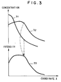
- Fig. 3 diagramatically shows a simulating method for obtaining the intensity of absorption of point-defects according to the fourth embodiment of the present invention.
- the different point of the fourth embodiment from the former three embodiments is that the ion implanting process is performed several times.
- a distribution of an initial concentration C i D (x) of point-defects, where i represents the serial number of each implantation process, is obtained using the ion implanting simulator for each ion implanting process as shown in Fig. 3 in which, for example, a couple of distributions are represented by curves 31 and 32.
- Fig. 4 diagramatically shows a simulating method for obtaining the intensity of absorption of point-defects according to the fifth embodiment of the present invention.
- the different point of the fifth embodiment from the former four embodiments is that another annealing is inserted between ion implanting process and the annealing under simulation.
- the distribution (represented by curve 41) of the initial concentration C D (x) of point-defects that generates when the ion implanting process is performed varies at the time when the another annealing is subsequently applied.
- the diffusion of impurities can be simulated in a two-dimensional space or a three-dimensional space as well as a one-dimensional space with a diffusion equation including a term representing the absorption of point-defects.
- the diffusion simulation can cope with various conditions of the ion implanting process such as multiple ion implantation and annealing after ion implantation, thus the practicability of the diffusion simulation can be enhanced.
- the present invention is a computer program executing in a computer system which comprises a central processing unit, a main memory, a secondary memory, and a bus connecting the central processing unit, the main memory, and the secondary memory.
- the computer program is stored in the secondary memory.
- the computer program resides in a main memory during execution.
- the computer program includes instructions which causes the central processing unit to perform the functions or methods explained above.
Landscapes
- Engineering & Computer Science (AREA)
- Physics & Mathematics (AREA)
- Theoretical Computer Science (AREA)
- Computer Hardware Design (AREA)
- Evolutionary Computation (AREA)
- Geometry (AREA)
- General Engineering & Computer Science (AREA)
- General Physics & Mathematics (AREA)
- Management, Administration, Business Operations System, And Electronic Commerce (AREA)
- Insulated Gate Type Field-Effect Transistor (AREA)
- Testing Or Measuring Of Semiconductors Or The Like (AREA)
Applications Claiming Priority (3)
| Application Number | Priority Date | Filing Date | Title |
|---|---|---|---|
| JP5755697 | 1997-03-12 | ||
| JP57556/97 | 1997-03-12 | ||
| JP5755697A JP3102374B2 (ja) | 1997-03-12 | 1997-03-12 | 拡散シミュレーション方法 |
Publications (2)
| Publication Number | Publication Date |
|---|---|
| EP0864992A2 true EP0864992A2 (de) | 1998-09-16 |
| EP0864992A3 EP0864992A3 (de) | 2000-03-01 |
Family
ID=13059099
Family Applications (1)
| Application Number | Title | Priority Date | Filing Date |
|---|---|---|---|
| EP98104401A Withdrawn EP0864992A3 (de) | 1997-03-12 | 1998-03-11 | Verfahren, Gerät und Rechnerprogrammprodukt zur Simulation der Diffusion von Verunreinigunen in einem Halbleiter |
Country Status (4)
| Country | Link |
|---|---|
| US (1) | US6154718A (de) |
| EP (1) | EP0864992A3 (de) |
| JP (1) | JP3102374B2 (de) |
| KR (1) | KR100297157B1 (de) |
Cited By (1)
| Publication number | Priority date | Publication date | Assignee | Title |
|---|---|---|---|---|
| WO2002080045A3 (en) * | 2001-03-28 | 2003-11-13 | California Inst Of Techn | De novo processing of electronic materials |
Families Citing this family (5)
| Publication number | Priority date | Publication date | Assignee | Title |
|---|---|---|---|---|
| US6697771B1 (en) * | 1999-06-30 | 2004-02-24 | Kabushiki Kaisha Toshiba | Semiconductor device manufacturing system and the method thereof |
| JP4991062B2 (ja) * | 2001-05-29 | 2012-08-01 | ラピスセミコンダクタ株式会社 | 半導体プロセスデバイスモデリング方法 |
| WO2007007402A1 (ja) * | 2005-07-13 | 2007-01-18 | Fujitsu Limited | イオン注入のシミュレーション方法及び半導体装置の製造方法 |
| JP5405055B2 (ja) * | 2008-06-18 | 2014-02-05 | ルネサスエレクトロニクス株式会社 | 半導体装置の解析及び設計装置、及び半導体装置の解析及び設計方法 |
| JP6135611B2 (ja) * | 2014-07-03 | 2017-05-31 | 信越半導体株式会社 | 点欠陥濃度計算方法、Grown−in欠陥計算方法、Grown−in欠陥面内分布計算方法及びこれらを用いたシリコン単結晶製造方法 |
Family Cites Families (4)
| Publication number | Priority date | Publication date | Assignee | Title |
|---|---|---|---|---|
| US4599118A (en) * | 1981-12-30 | 1986-07-08 | Mostek Corporation | Method of making MOSFET by multiple implantations followed by a diffusion step |
| US5504016A (en) * | 1991-03-29 | 1996-04-02 | National Semiconductor Corporation | Method of manufacturing semiconductor device structures utilizing predictive dopant-dopant interactions |
| JPH06283458A (ja) * | 1993-03-30 | 1994-10-07 | Toshiba Corp | シミュレーション方法及びシミュレーション装置 |
| JP2713212B2 (ja) * | 1995-03-13 | 1998-02-16 | 日本電気株式会社 | 拡散シミュレーション方法 |
-
1997
- 1997-03-12 JP JP5755697A patent/JP3102374B2/ja not_active Expired - Fee Related
-
1998
- 1998-03-11 EP EP98104401A patent/EP0864992A3/de not_active Withdrawn
- 1998-03-12 KR KR1019980008294A patent/KR100297157B1/ko not_active Expired - Fee Related
- 1998-03-12 US US09/041,504 patent/US6154718A/en not_active Expired - Fee Related
Cited By (1)
| Publication number | Priority date | Publication date | Assignee | Title |
|---|---|---|---|---|
| WO2002080045A3 (en) * | 2001-03-28 | 2003-11-13 | California Inst Of Techn | De novo processing of electronic materials |
Also Published As
| Publication number | Publication date |
|---|---|
| JPH10256174A (ja) | 1998-09-25 |
| KR19980080183A (ko) | 1998-11-25 |
| EP0864992A3 (de) | 2000-03-01 |
| JP3102374B2 (ja) | 2000-10-23 |
| US6154718A (en) | 2000-11-28 |
| KR100297157B1 (ko) | 2001-08-07 |
Similar Documents
| Publication | Publication Date | Title |
|---|---|---|
| US5761481A (en) | Semiconductor simulator tool for experimental N-channel transistor modeling | |
| US6360190B1 (en) | Semiconductor process device simulation method and storage medium storing simulation program | |
| EP0864992A2 (de) | Verfahren, Gerät und Rechnerprogrammprodukt zur Simulation der Diffusion von Verunreinigunen in einem Halbleiter | |
| JP2783174B2 (ja) | イオン注入不純物分布のシミュレーション方法 | |
| US5889687A (en) | Simulator, simulation and fabrication methods of semiconductor device and storage medium storing program for executing the simulation method | |
| US11973868B2 (en) | Systems and methods for a fast near-field electromagnetic simulation methodology for side-channel emission analysis | |
| EP0867818A2 (de) | Verfahren, Gerät und Rechnerprogrammprodukt zur Simulation einer Ionenimplantierung | |
| US5784302A (en) | High speed point defect diffusion simulating method | |
| JP3050290B2 (ja) | アモルファス化領域決定方法 | |
| US5504016A (en) | Method of manufacturing semiconductor device structures utilizing predictive dopant-dopant interactions | |
| CN118395683B (zh) | 基于非参数解集的太阳能辐照度概率建模方法及装置 | |
| EP0701221A2 (de) | Verfahren zur Bestimmung von Potential-Anfangswerten in Halbleiterbaustein-Simulation | |
| Senez et al. | 3-dimensional simulation of thermal diffusion and oxidation processes | |
| JP2000150659A (ja) | 半導体集積回路装置のレイアウト設計方法 | |
| JP3266113B2 (ja) | イオン注入プロセスのシミュレーション方法 | |
| Ebert et al. | Efficient Shape Uncertainty Quantification for the TESLA Cavity | |
| Penumalli | Computer simulation in VLSI process modeling | |
| US6148276A (en) | Diffusion simulating method | |
| JPH11162863A (ja) | 半導体シミュレーション方法 | |
| Coelho et al. | High-Speed Electrothermal Simulations for Power Modules with PEEC and Thermal Resistance Networks | |
| JPH07105267A (ja) | 半導体装置の設計方法 | |
| JPH06290240A (ja) | シミュレーション方法 | |
| JPH07147254A (ja) | 高速三次元不純物分布計算方法 | |
| Balamurugan et al. | Improved analytic models and efficient parameter extraction for computationally efficient 1D and 2D ion implantation modeling | |
| JPH09270391A (ja) | イオン注入プロセスのシミュレーション方法 |
Legal Events
| Date | Code | Title | Description |
|---|---|---|---|
| PUAI | Public reference made under article 153(3) epc to a published international application that has entered the european phase |
Free format text: ORIGINAL CODE: 0009012 |
|
| AK | Designated contracting states |
Kind code of ref document: A2 Designated state(s): CH DE GB LI |
|
| AX | Request for extension of the european patent |
Free format text: AL;LT;LV;MK;RO;SI |
|
| PUAL | Search report despatched |
Free format text: ORIGINAL CODE: 0009013 |
|
| AK | Designated contracting states |
Kind code of ref document: A3 Designated state(s): AT BE CH DE DK ES FI FR GB GR IE IT LI LU MC NL PT SE |
|
| AX | Request for extension of the european patent |
Free format text: AL;LT;LV;MK;RO;SI |
|
| 17P | Request for examination filed |
Effective date: 20000118 |
|
| AKX | Designation fees paid |
Free format text: CH DE GB LI |
|
| RAP1 | Party data changed (applicant data changed or rights of an application transferred) |
Owner name: NEC ELECTRONICS CORPORATION |
|
| STAA | Information on the status of an ep patent application or granted ep patent |
Free format text: STATUS: THE APPLICATION HAS BEEN WITHDRAWN |
|
| 18W | Application withdrawn |
Effective date: 20031126 |