EP0865683B1 - Serieller multi-gb/s datenempfänger - Google Patents
Serieller multi-gb/s datenempfänger Download PDFInfo
- Publication number
- EP0865683B1 EP0865683B1 EP96910879A EP96910879A EP0865683B1 EP 0865683 B1 EP0865683 B1 EP 0865683B1 EP 96910879 A EP96910879 A EP 96910879A EP 96910879 A EP96910879 A EP 96910879A EP 0865683 B1 EP0865683 B1 EP 0865683B1
- Authority
- EP
- European Patent Office
- Prior art keywords
- data pulse
- collector
- input
- transistor
- pair
- Prior art date
- Legal status (The legal status is an assumption and is not a legal conclusion. Google has not performed a legal analysis and makes no representation as to the accuracy of the status listed.)
- Expired - Lifetime
Links
Images

Classifications
-
- H—ELECTRICITY
- H03—ELECTRONIC CIRCUITRY
- H03K—PULSE TECHNIQUE
- H03K3/00—Circuits for generating electric pulses; Monostable, bistable or multistable circuits
- H03K3/02—Generators characterised by the type of circuit or by the means used for producing pulses
- H03K3/023—Generators characterised by the type of circuit or by the means used for producing pulses by the use of differential amplifiers or comparators, with internal or external positive feedback
- H03K3/0233—Bistable circuits
- H03K3/02337—Bistables with hysteresis, e.g. Schmitt trigger
Definitions
- This invention relates to a data receiver and more particularly to a receiver for detecting and amplifying low level data pulses.
- EMI electromagnetic interference
- One technique that has been employed successfully to reduce the number of interconnections and EMI in communications switching equipment involves a contactless backplane. This technique is based on directional coupling principles wherein data transfer occurs between proximate conductors.
- An example of one such coupling connector is described in U.S. Patent 5,432,486 which issued July 11, 1995 to Wong and assigned to Northern Telecom Limited. The technique can be expanded to permit point-to-multipoint and multipoint-to-point data transmission over a passive backplane without loss of signal integrity due to multipoint connectors.
- distribution of the multi gigabit-per-second serial data employs a form of a.c. coupling, of such small proportions, that the data information is contained in the data transitions.
- a data signal in NRZ format on the transmission path is coupled to the receiver path as positive and negative going pulses.
- the received data at the demultiplex circuit is considerably attenuated: signal levels of only 70 mV peak-to-peak, or less, are not uncommon.
- the present invention relates to the requirement of detecting serial data at gigabit-per-second rates received over a transmission medium through which the signal levels have been substantially attenuated.
- a data pulse receiver comprising: a grounded base amplifier having a bipolar transistor with a base, a collector and an emitter, said base being connected to a.c. ground; an input connected to said emitter for receiving said data pulse, said input having impedance matching means; a constant current source between said emitter and ground; a load resistor between said collector and a positive supply; hysteresis generating means connected to said collector and said hysteresis generating means having a current supply; and an output terminal (76) between said collector and load resistor to deliver an amplified data pulse output.
- the receiver employs a pair of grounded base amplifiers, each with its own current source, in order to accept a differential input.
- the hysteresis generating means includes a set-reset flip flop.
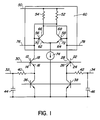
- FIGURE 1 is a circuit diagram of one embodiment of the present invention.
- the receiver includes grounded base amplifier 12 having base 14, emitter 16 and collector 18, and grounded base amplifier 22 having base 24, emitter 26 and collector 28.
- Bases 14 and 24 are connected to a.c. ground at 30.
- FIGURE 1 is based on a differential input and to this end the coupled data pulses in differential format are supplied to negative input 32 and positive input 34. It is to be understood that the input need not be differential in which case the receiver would have a single input and a single grounded base amplifier.
- Grounded base amplifiers 12 and 22 have constant current sources 36 and 38 respectively. Also shown in FIGURE 1 are input impedance matching resistors 40 and 42. Capacitors 44 and 46 represent stray capacitance inherent in the structure.
- the collectors 18 and 28 of transistors 12 and 22 respectively are connected to a positive source 50 through load resistors 52 and 54 respectively.
- Load resistors 52 and 54 in combination with bipolar transistors 56 and 58 form a regenerating flip-flop 60.
- Regenerating flip-flop 60 reconverts the Return to Zero RZ pulse signal to the required NRZ format.
- Transistors 56 and 58 include commonly connected emitters 62 and 64, collectors 66 and 68, and bases 70,72.
- the commonly connected emitters 62,64 are provided with tail current by current source 74.
- Positive and negative output pulses are provided at terminals 76 and 78 respectively.
- the circuit of FIGURE 1 obtains a matching impedance of, for example, 50 ohms by means of resistors 40 and 42 in the input circuit together with the input impedance of the grounded base differential amplifiers 12 and 22.
- the circuit has the largest possible bandwidth due to the use of the grounded base transistors. Also from Kirchoff's Law, it is clear that, apart from the effect of parasitic components, the entire signal energy is utilized by the grounded base amplifier. Further, the effect of parasitic capacitance on the input terminals, which would normally shunt the input signal, is compensated by the inductance seen at the emitter of the grounded base amplifier. This latter effect significantly extends the frequency response of the amplifier. Design of the grounded base amplifier is as follows:
- the maximum pulse level is 120mV (single ended) and the minimum pulse level is 70 mV.
- Error(%) 100*0.019*((1/(Ie-(Vp/50)))-(1/Ie))/50 where Ie is the emitter bias current and Vp is the pulse amplitude.
- the transistors of the grounded base amplifier will in general be quite large, in order to withstand electrostatic discharge potentials. Normally this protection will be augmented by means of parallel diodes (not shown). As a result, due to the size of the transistors, the effect of parasitic emitter and base resistance has been neglected since these will be quite small. The above results have been plotted in FIGURE 4, showing the variation of impedance mismatch for various signal levels against the amplifier bias current.
- the grounded base amplifiers 12,22 are connected to a set-reset flip-flop 60.
- the magnitude of the tail current of the flip-flop 60 can be adjusted by current supply 74 to obtain a controlled amount of hysteresis. Specifically, the tail current can be adjusted to whatever threshold current is specified for the detection of the input signal current. It will be noted from FIGURE 1 that due to the grounded base amplifiers, the input signal current passes through the collector load resistors 52,54 of the flip-flop 60. Also, the tail current of the flip-flop 60 passes through the same collector load resistors.
- the voltage produced by the current pulses in the collector resistors 52,54 must exceed the voltage established by the tail current of the flip-flop in the same resistors.
- the tail current can be easily adjusted by means of an external resistor or wired connection, to suit a particular application. Note that the contribution of the currents from both amplifier inputs must be taken into account, assuming the input signal to be differential. If the input signal is only applied to one input of the amplifier, the tail current must be halved for the same amount of hysteresis. Under normal circumstances the input signal will be differential so as to make the circuit substantially immune to common mode input noise. It can be shown from standard communications theory that the required input noise level relative to the hysteresis level must be of the order of -24dB to obtain a transmission bit error rate of one error in 10 -14 .
- a pulse current of 1 mA is transported by both grounded base amplifier emitter collector circuits, and the bias current level of the RS flip-flop must be 2mA.
- To match the input impedance between 40 to 60 under maximum signal conditions would require a total power supply current of 5mA (or a power of 15mW at 3 volt power supply).
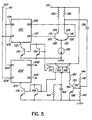
- FIGURE 5 represents a particular application of the signal data receiver of the present invention.
- the level of the input signal or data at line 102 and 104 is either not known or is variable. Under these conditions a fixed hysteresis level is undesirable since an optimum bit error rate cannot generally be obtained. To overcome this difficulty it is desirable to monitor the level of the incoming data signal and to adjust the hysteresis level by automatic means.
- a target specification for this data receiver is that it should be able to detect incoming data pulses with a peak amplitude of 30 mV and pulse duration exceeding the hysteresis level of not less than 100ps.
- the energy present in such data pulses is so small that monitoring the level accurately presents some difficulty.
- recall that the data pulses are converted immediately from RZ (return to zero) format to NRZ format (non-return to zero) by the pulse receiver circuit. Direct monitoring of the amplitude of the input data stream has in fact not been possible.
- an alternative scheme has been employed which successfully monitors the input pulse height very accurately and enables optimum adjustment of the hysteresis level.
- the pulse height at the output of the pulse receiver is primarily determined by the level of the hysteresis bias current to the set-reset flip-flop of FIGURE 1. Therefore, at the output of the set-reset flip-flop there is no amplitude information about the incoming data stream. This flip-flop will toggle, provided that the input data signal magnitude exceeds the hysteresis level by an unknown amount. If the output of the flip-flop is connected to a differential pair, then the output of the differential pair will also toggle, if the flip-flop toggles. Further, common mode variations at the output of the flip-flop are not present at the output of the differential pair.
- the presence or absence of pulses at the output of the differential pair can be taken to indicate that the hysteresis level is either less than or greater than the incoming data pulse magnitude.
- a.c. coupling the output of the differential pair to a rectifier circuit one obtains a signal whose magnitude is either large, or very small, depending on whether the hysteresis level is less than or greater than the incoming data pulse peak magnitude.
- a voltage is obtained which can be used to adjust the level of the hysteresis bias current. The net result is an automatic hysteresis adjustment which continually adjusts the data pulse receiver hysteresis level to the level of the data pulses.
- a second data pulse receiver is utilized in parallel with the one which monitors the data pulse magnitude, and the hysteresis level of the second data pulse receiver is set to a proportionate lower value of that of the monitoring receiver. It is possible in fact to set the hysteresis level of the second data pulse receiver to be any desired proportion of the peak height of the data pulse, a level of 50% usually results in optimum bit error rate performance.
- two data pulse receivers are connected in parallel, their individual input impedances are adjusted to provide a proper combined input termination impedance.
- FIGURE 5 illustrates schematically a data pulse receiver with automatic hysteresis adjustment.
- the data pulses are transferred to the receiver via lines 100,101.
- the receiver illustrated in FIGURE 1 is box 102 in FIGURE 5.
- the differential pulse input is supplied at input terminals 104 and 106.
- the receiver output is taken from terminals 108 and 110 while the current sink for this receiver is supplied at terminal 112.
- Pulse receiver 102 is used to monitor the data level.
- Pulse receiver 202 having input 204,206, outputs 208,210 and hysteresis current 212, is used to receive the data with very low bit-error-rate.
- transistors 116, 118, 172, 174, 176 and 178 are all the same size.
- P-channel field effect transistors 166,168 and 170 have different sizes: in particular the ratio of the transconductance of transistors 170 and 168 determines the ratio of the current sink from receivers 102,202 respectively.
- Transistor pairs 172,174 and 176,178 are 1:1 mirrors used for monitoring the current sourced by transistors 170,168 respectively. Further, if the transconductance of transistor 166 is less than that of transistor 168 then the P-channel FET mirror of 166,168 will exhibit current gain. This is of advantage in increasing the accuracy of the pulse height detector circuit.
- transistors, 166,168 and 170 have equal channel length and channel widths in the ratio 1:5:10 respectively.
- the hysteresis level of pulse receiver 202 will be set to half the data peak amplitude.
- the differential output of receiver 102 is supplied to differential pair 116,118 at bases 120,122, respectively.
- Emitters 128,130 are connected to bias current source 132.
- Collectors 124,126 are connected to a positive supply 135 via load resistors 134,136 respectively.
- the differential pair 116,118 will switch if the output of pulse receiver 102 switches. This will occur if the data pulse peak magnitude is greater than the hysteresis level of the pulse receiver 102.
- An output of differential pair 116,118 is taken from load resistor 136 and is a.c. coupled via capacitor 138 to the detector circuit comprising resistors 140,142 and transistor 150. In a practical circuit one might also utilize the output from load resistor 134 with an additional parallel connected detector circuit, thereby increasing the sensitivity of the circuit.
- the second detector circuit is not shown in FIGURE 5 for the sake of simplicity.
- the detection circuit of resistors 140,142 and transistor 150 is biased by means of a reference voltage at 144 and the ratio of resistors 140 and 142 so that the voltage at base 152 is just less than a diode voltage drop, say about 0.75 volts.
- pulses are coupled via capacitor 138 to base 152 of transistor 150, they momentarily increase the potential on base 152 and thereby cause transistor 150 to conduct current and so to lower the gate potential of FET 166.
- Capacitor 162 in conjunction with resistor 160 is used to integrate the pulsed current from transistor 150, so that transistors 166,168 and 170 conduct a slowly varying current. The minimum value of the current in these transistors is set by resistor 164 which therefore sets the minimum hysteresis level.
Landscapes
- Dc Digital Transmission (AREA)
- Manipulation Of Pulses (AREA)
Claims (11)
- Datenimpulsempfänger mit:einem Verstärker (12) mit geerdeter Basis, der einen bipolaren Transistor mit einer Basis (14), einem Kollektor (18) und einem Emitter (16) aufweist, wobei die Basis (14) mit Wechselspannungserde (30) verbunden ist;einem Eingang (32), der mit dem Emitter verbunden ist, um den Datenimpuls zu empfangen, wobei der Eingang eine Impedanzanpaßeinrichtung (40) aufweist;eine Konstantstromquelle (36), die zwischen dem Emitter und Erde eingeschaltet ist;einem Lastwiderstand (52) zwischen dem Kollektor und einer positiven Versorgung (50);eine Hysterese erzeugende Einrichtungen (60), die mit dem Kollektor verbunden sind, wobei die die Hysterese erzeugenden Einrichtungen eine Stromversorgung (74) aufweisen; undeinen Ausgangsanschluß (76) zwischen dem Kollektor und dem Lastwiderstand zur Lieferung eines verstärkten Datenimpuls-Ausganges.
- Datenimpulsempfänger nach Anspruch 1, der ein Paar von Verstärkern (12, 22) mit geerdeter Basis aufweist, die zum Empfang eines Differenzeinganges verbunden sind.
- Datenimpulsempfänger nach Anspruch 1 oder 2, wobei der Datenimpuls eine Spitzenamplitude von zumindest 30 mV und eine Impulsdauer von zumindest 100 ps aufweist.
- Datenimpulsempfänger nach Anspruch 1, bei dem die die Hysterese erzeugenden Einrichtungen eine regenerative Flipflopschaltung (60) zur Umwandlung einer Impulsschwingungsform mit Rückkehr auf Null in eine Datenschwingungsform ohne Rückkehr auf Null umfassen.
- Datenimpulsempfänger nach einem der vorhergehenden Ansprüche, dadurch gekennzeichnet, daß die Stromversorgung (74) für die die Hysterese erzeugenden Einrichtungen (60) programmierbar ist, um so selektiv Eingangssignalstörungen zu unterdrücken.
- Datenimpulsempfänger nach einem der vorhergehenden Ansprüche, der automatische Hysterese-Einstelleinrichtungen aufweist.
- Datenimpulsempfänger nach Anspruch 6, bei dem der Datenimpuls-Ausgang mit einem Differenzpaar (116, 118) gekoppelt ist, das einen impulsförmigen Ausgang liefert, dessen Vorhandensein davon abhängt, daß der Hysterese-Pegel kleiner als die Amplitude der ankommenden Datenimpulse ist.
- Datenimpulsempfänger nach Anspruch 7, bei dem der impulsförmige Ausgang von dem Differenzpaar wechselspannungsmäßig mit einer Gleichrichterschaltung (136, 138) gekoppelt ist.
- Datenimpulsempfänger nach Anspruch 8, bei dem die Gleichrichterschaltung ein Ausgangssignal liefert, das in einer Integrationsschaltung (150, 160, 162) integriert wird, um eine Gleichspannung zu gewinnen, die zur Einstellung des Pegels des Hysterese-Vorstromes verwendet wird.
- Datenimpulsempfänger nach Anspruch 9, in Kombination mit einem zweiten Datenimpulsempfänger, der zum Empfang des Eingangsdatenimpulses parallel zu dem ersten Impulsempfänger angeschaltet ist, wobei dem zweiten Datenimpulsempfänger ein Hysterese-Vorstrom zugeführt wird, dessen Pegel ein voreingestelltes Verhältnis des Hysterese-Vorstromes ist, der dem ersten Impulsempfänger zugeführt wird.
- Datenimpulsempfänger nach Anspruch 1, bei dem:der Verstärker (12) mit geerdeter Basis ein Paar von bipolaren Transistoren (12, 22) aufweist, wobei jeder der Transistoren eine Basis (14, 24), einen Kollektor (18, 28) und einen Emitter (16, 26) aufweist, wobei die Basen mit Wechselspannungserde (30) verbunden sind;mit zwei Eingängen (32, 34), wobei der erste Eingang (32) mit dem Emitter (16) des ersten Transistors (12) des Paares von bipolaren Transistoren verbunden ist, wobei der erste Eingang Impedanzanpaßeinrichtungen (40) aufweist, und wobei der zweite Eingang (34) mit dem Emitter (26) des zweiten Transistors (22) des Paares von bipolaren Transistoren verbunden ist, wobei der zweite Eingang Impedanzanpaßeinrichtungen (42) aufweist;mit zwei Konstantstromquellen (36, 38) wobei die ersten Konstantstromquelle (36) zwischen dem Emitter des ersten Transistors des Paares von bipolaren Transistoren und Erde eingeschaltet ist, und wobei die zweite Konstantstromquelle (38) zwischen dem Emitter des zweiten Transistors des Paares von bipolaren Transistoren und Erde eingeschaltet ist;mit zwei Lasteingängen (52, 54), wobei der erste Lastwiderstand (52) zwischen dem Kollektor des ersten Transistors des Paares von bipolaren Transistoren und einer positiven Versorgung (50) eingeschaltet ist, und wobei der zweite Lastwiderstand (54) zwischen dem Kollektor des zweiten Transistors des Paares von bipolaren Transistoren und einer positiven Versorgung eingeschaltet ist;mit eine Hysterese erzeugenden Einrichtungen (60) mit einer Stromversorgung (74) und einer Setz-Rücksetz-Flipflopschaltung, wobei die die Hysterese erzeugenden Einrichtungen mit dem Kollektor des ersten Transistors und dem Kollektor des zweiten Transistors verbunden sind; undmit zwei Ausgangsanschlüssen (76, 78), wobei der erste Ausgangsanschluß mit dem Kollektor des ersten Transistors des Paares von bipolaren Transistoren verbunden ist, während der zweite Ausgangsanschluß mit dem Kollektor des zweiten Transistors des Paares von bipolaren Transistoren verbunden ist.
Applications Claiming Priority (3)
| Application Number | Priority Date | Filing Date | Title |
|---|---|---|---|
| US08/568,911 US5852637A (en) | 1995-12-07 | 1995-12-07 | Serial multi-GB/s data receiver |
| US568911 | 1995-12-07 | ||
| PCT/CA1996/000271 WO1997021270A1 (en) | 1995-12-07 | 1996-05-01 | Serial multi-gb/s data receiver |
Publications (2)
| Publication Number | Publication Date |
|---|---|
| EP0865683A1 EP0865683A1 (de) | 1998-09-23 |
| EP0865683B1 true EP0865683B1 (de) | 2002-08-14 |
Family
ID=24273267
Family Applications (1)
| Application Number | Title | Priority Date | Filing Date |
|---|---|---|---|
| EP96910879A Expired - Lifetime EP0865683B1 (de) | 1995-12-07 | 1996-05-01 | Serieller multi-gb/s datenempfänger |
Country Status (6)
| Country | Link |
|---|---|
| US (1) | US5852637A (de) |
| EP (1) | EP0865683B1 (de) |
| JP (1) | JPH11506290A (de) |
| CA (1) | CA2235591C (de) |
| DE (1) | DE69623037T2 (de) |
| WO (1) | WO1997021270A1 (de) |
Families Citing this family (12)
| Publication number | Priority date | Publication date | Assignee | Title |
|---|---|---|---|---|
| US6058144A (en) * | 1998-04-03 | 2000-05-02 | Nortel Networks Corporation | Multi-GB/S data pulse receiver |
| US6272185B1 (en) * | 1998-05-04 | 2001-08-07 | Nortel Networks Limited | Method and apparatus for performing data pulse detection |
| US6529564B1 (en) * | 1999-01-28 | 2003-03-04 | Nortel Networks Limited | Data pulse receiver |
| US6751217B1 (en) * | 1999-10-06 | 2004-06-15 | Nortel Networks Limited | Combined selector switch and serial multi-Gb/s data pulse receiver |
| US7124221B1 (en) | 1999-10-19 | 2006-10-17 | Rambus Inc. | Low latency multi-level communication interface |
| US6396329B1 (en) | 1999-10-19 | 2002-05-28 | Rambus, Inc | Method and apparatus for receiving high speed signals with low latency |
| US7161513B2 (en) | 1999-10-19 | 2007-01-09 | Rambus Inc. | Apparatus and method for improving resolution of a current mode driver |
| US6956905B1 (en) * | 2000-03-23 | 2005-10-18 | Xilinx, Inc. | Peak detector circuit |
| US7778351B2 (en) * | 2002-04-09 | 2010-08-17 | International Business Machines Corporation | Tunable CMOS receiver apparatus |
| US8861667B1 (en) | 2002-07-12 | 2014-10-14 | Rambus Inc. | Clock data recovery circuit with equalizer clock calibration |
| US8319756B2 (en) * | 2002-11-15 | 2012-11-27 | Entropic Communications, Inc. | Adaptive hysteresis for reduced swing signalling circuits |
| JP5293320B2 (ja) * | 2009-03-23 | 2013-09-18 | 富士通セミコンダクター株式会社 | 受信回路 |
Citations (1)
| Publication number | Priority date | Publication date | Assignee | Title |
|---|---|---|---|---|
| US4599602A (en) * | 1983-08-03 | 1986-07-08 | Matsushita Electric Industrial Co., Ltd. | Serial-type A/D converter utilizing folding circuit cells |
Family Cites Families (7)
| Publication number | Priority date | Publication date | Assignee | Title |
|---|---|---|---|---|
| US4259601A (en) * | 1978-12-08 | 1981-03-31 | Motorola, Inc. | Comparison circuit having bidirectional hysteresis |
| US4488063A (en) * | 1979-11-19 | 1984-12-11 | Burroughs Corporation | EFL Latch merged with decoder-multiplexer |
| US4386282A (en) * | 1980-09-29 | 1983-05-31 | Bell Telephone Laboratories, Incorporated | Emitter function logic (EFL) shift register |
| US4728818A (en) * | 1986-12-17 | 1988-03-01 | Tandem Computers Incorporated | Emitter function logic with concurrent, complementary outputs |
| US4970412A (en) * | 1989-07-28 | 1990-11-13 | Motorola, Inc. | Comparator circuit |
| JPH06101671B2 (ja) * | 1989-09-27 | 1994-12-12 | 株式会社東芝 | 電圧比較回路 |
| US5432486A (en) * | 1993-05-20 | 1995-07-11 | Northern Telecom Limited | Capacitive and inductive coupling connector |
-
1995
- 1995-12-07 US US08/568,911 patent/US5852637A/en not_active Expired - Lifetime
-
1996
- 1996-05-01 WO PCT/CA1996/000271 patent/WO1997021270A1/en not_active Ceased
- 1996-05-01 JP JP9520809A patent/JPH11506290A/ja active Pending
- 1996-05-01 CA CA002235591A patent/CA2235591C/en not_active Expired - Fee Related
- 1996-05-01 DE DE69623037T patent/DE69623037T2/de not_active Expired - Fee Related
- 1996-05-01 EP EP96910879A patent/EP0865683B1/de not_active Expired - Lifetime
Patent Citations (1)
| Publication number | Priority date | Publication date | Assignee | Title |
|---|---|---|---|---|
| US4599602A (en) * | 1983-08-03 | 1986-07-08 | Matsushita Electric Industrial Co., Ltd. | Serial-type A/D converter utilizing folding circuit cells |
Also Published As
| Publication number | Publication date |
|---|---|
| DE69623037D1 (de) | 2002-09-19 |
| CA2235591A1 (en) | 1997-06-12 |
| US5852637A (en) | 1998-12-22 |
| WO1997021270A1 (en) | 1997-06-12 |
| JPH11506290A (ja) | 1999-06-02 |
| EP0865683A1 (de) | 1998-09-23 |
| CA2235591C (en) | 2000-07-18 |
| DE69623037T2 (de) | 2002-12-12 |
Similar Documents
| Publication | Publication Date | Title |
|---|---|---|
| US6272185B1 (en) | Method and apparatus for performing data pulse detection | |
| US6768352B1 (en) | Low voltage receiver circuit and method for shifting the differential input signals of the receiver depending on a common mode voltage of the input signals | |
| US6037841A (en) | Impedance matched CMOS transimpedance amplifier for high-speed fiber optic communications | |
| US6130548A (en) | Signal converting receiver having constant hysteresis, and method therefor | |
| US5977819A (en) | CMOS gigabit serial link differential transmitter and receiver | |
| US8599966B2 (en) | Coupling system for data receivers | |
| US5852637A (en) | Serial multi-GB/s data receiver | |
| US10949375B2 (en) | Methods and apparatus for an interface | |
| EP1068667B1 (de) | Mehrfach-gb/s datenpulsempfänger | |
| US5153466A (en) | All monolithic transceiver operative from a low voltage vcc dc supply | |
| US5050190A (en) | Signal detection circuit not affected by minute voltage fluctuations contained in input signal and operation method therefor | |
| JP4237402B2 (ja) | 対称送信ライン駆動用出力バッファ | |
| EP1145426B1 (de) | Datenimpulsempfänger | |
| US4817208A (en) | Fiber optic receiver | |
| US5625648A (en) | Signal receiving and signal processing unit | |
| US6628721B1 (en) | Simplified differential signaling | |
| US20040264582A1 (en) | Method for reducing DC offset error for single ended and differential signals | |
| MXPA96003708A (en) | Unit of reception and processing of sign |
Legal Events
| Date | Code | Title | Description |
|---|---|---|---|
| PUAI | Public reference made under article 153(3) epc to a published international application that has entered the european phase |
Free format text: ORIGINAL CODE: 0009012 |
|
| 17P | Request for examination filed |
Effective date: 19980707 |
|
| AK | Designated contracting states |
Kind code of ref document: A1 Designated state(s): DE FR GB |
|
| RAP3 | Party data changed (applicant data changed or rights of an application transferred) |
Owner name: NORTEL NETWORKS CORPORATION |
|
| RAP1 | Party data changed (applicant data changed or rights of an application transferred) |
Owner name: NORTEL NETWORKS LIMITED |
|
| 17Q | First examination report despatched |
Effective date: 20001129 |
|
| GRAG | Despatch of communication of intention to grant |
Free format text: ORIGINAL CODE: EPIDOS AGRA |
|
| GRAG | Despatch of communication of intention to grant |
Free format text: ORIGINAL CODE: EPIDOS AGRA |
|
| GRAH | Despatch of communication of intention to grant a patent |
Free format text: ORIGINAL CODE: EPIDOS IGRA |
|
| GRAH | Despatch of communication of intention to grant a patent |
Free format text: ORIGINAL CODE: EPIDOS IGRA |
|
| GRAA | (expected) grant |
Free format text: ORIGINAL CODE: 0009210 |
|
| AK | Designated contracting states |
Kind code of ref document: B1 Designated state(s): DE FR GB |
|
| REG | Reference to a national code |
Ref country code: GB Ref legal event code: FG4D |
|
| REF | Corresponds to: |
Ref document number: 69623037 Country of ref document: DE Date of ref document: 20020919 |
|
| ET | Fr: translation filed | ||
| PLBE | No opposition filed within time limit |
Free format text: ORIGINAL CODE: 0009261 |
|
| STAA | Information on the status of an ep patent application or granted ep patent |
Free format text: STATUS: NO OPPOSITION FILED WITHIN TIME LIMIT |
|
| 26N | No opposition filed |
Effective date: 20030515 |
|
| PGFP | Annual fee paid to national office [announced via postgrant information from national office to epo] |
Ref country code: GB Payment date: 20040422 Year of fee payment: 9 |
|
| PGFP | Annual fee paid to national office [announced via postgrant information from national office to epo] |
Ref country code: FR Payment date: 20040503 Year of fee payment: 9 |
|
| PGFP | Annual fee paid to national office [announced via postgrant information from national office to epo] |
Ref country code: DE Payment date: 20040528 Year of fee payment: 9 |
|
| PG25 | Lapsed in a contracting state [announced via postgrant information from national office to epo] |
Ref country code: GB Free format text: LAPSE BECAUSE OF NON-PAYMENT OF DUE FEES Effective date: 20050501 |
|
| PG25 | Lapsed in a contracting state [announced via postgrant information from national office to epo] |
Ref country code: DE Free format text: LAPSE BECAUSE OF NON-PAYMENT OF DUE FEES Effective date: 20051201 |
|
| GBPC | Gb: european patent ceased through non-payment of renewal fee |
Effective date: 20050501 |
|
| PG25 | Lapsed in a contracting state [announced via postgrant information from national office to epo] |
Ref country code: FR Free format text: LAPSE BECAUSE OF NON-PAYMENT OF DUE FEES Effective date: 20060131 |
|
| REG | Reference to a national code |
Ref country code: FR Ref legal event code: ST Effective date: 20060131 |