EP0866558A2 - Programmbares logisches Feld mit als Produktterm konfigurierbarem Speicher mit wahlfreiem Zugriff - Google Patents
Programmbares logisches Feld mit als Produktterm konfigurierbarem Speicher mit wahlfreiem Zugriff Download PDFInfo
- Publication number
- EP0866558A2 EP0866558A2 EP98302057A EP98302057A EP0866558A2 EP 0866558 A2 EP0866558 A2 EP 0866558A2 EP 98302057 A EP98302057 A EP 98302057A EP 98302057 A EP98302057 A EP 98302057A EP 0866558 A2 EP0866558 A2 EP 0866558A2
- Authority
- EP
- European Patent Office
- Prior art keywords
- programmable logic
- logic device
- random access
- access memory
- circuitry
- Prior art date
- Legal status (The legal status is an assumption and is not a legal conclusion. Google has not performed a legal analysis and makes no representation as to the accuracy of the status listed.)
- Withdrawn
Links
Images




Classifications
-
- H—ELECTRICITY
- H03—ELECTRONIC CIRCUITRY
- H03K—PULSE TECHNIQUE
- H03K19/00—Logic circuits, i.e. having at least two inputs acting on one output; Inverting circuits
- H03K19/02—Logic circuits, i.e. having at least two inputs acting on one output; Inverting circuits using specified components
- H03K19/173—Logic circuits, i.e. having at least two inputs acting on one output; Inverting circuits using specified components using elementary logic circuits as components
- H03K19/177—Logic circuits, i.e. having at least two inputs acting on one output; Inverting circuits using specified components using elementary logic circuits as components arranged in matrix form
- H03K19/17748—Structural details of configuration resources
- H03K19/1776—Structural details of configuration resources for memories
-
- H—ELECTRICITY
- H03—ELECTRONIC CIRCUITRY
- H03K—PULSE TECHNIQUE
- H03K19/00—Logic circuits, i.e. having at least two inputs acting on one output; Inverting circuits
- H03K19/02—Logic circuits, i.e. having at least two inputs acting on one output; Inverting circuits using specified components
- H03K19/173—Logic circuits, i.e. having at least two inputs acting on one output; Inverting circuits using specified components using elementary logic circuits as components
- H03K19/177—Logic circuits, i.e. having at least two inputs acting on one output; Inverting circuits using specified components using elementary logic circuits as components arranged in matrix form
- H03K19/17724—Structural details of logic blocks
- H03K19/17728—Reconfigurable logic blocks, e.g. lookup tables
-
- H—ELECTRICITY
- H03—ELECTRONIC CIRCUITRY
- H03K—PULSE TECHNIQUE
- H03K19/00—Logic circuits, i.e. having at least two inputs acting on one output; Inverting circuits
- H03K19/02—Logic circuits, i.e. having at least two inputs acting on one output; Inverting circuits using specified components
- H03K19/173—Logic circuits, i.e. having at least two inputs acting on one output; Inverting circuits using specified components using elementary logic circuits as components
- H03K19/177—Logic circuits, i.e. having at least two inputs acting on one output; Inverting circuits using specified components using elementary logic circuits as components arranged in matrix form
- H03K19/17704—Logic circuits, i.e. having at least two inputs acting on one output; Inverting circuits using specified components using elementary logic circuits as components arranged in matrix form the logic functions being realised by the interconnection of rows and columns
Definitions
- This invention relates to programmable logic array devices having embedded random access memory arrays which can be configured as programmable product-term-type logic elements if desired. More particularly, the invention relates to programmable logic devices having look-up tables for performing logic and larger blocks of random access memory which are usable by the user for such purposes as data storage and additional look-up table logic, and which larger blocks of random access memory are alternatively configurable as programmable product-term-type logic elements.
- One known type of programmable logic device includes an array of programmable AND gates which typically produces multiple outputs, each generally resulting from the ANDing of multiple inputs. These AND gate array outputs are commonly referred to as "product terms" because the logical representation of the AND function is analogous to multiplication. Generally, a plurality of these product terms, or “p-terms,” are combined by an OR gate to produce a sum-of-products output (the OR function being analogous to addition).
- Another type of programmable logic device is implemented using many relatively small look-up tables whose inputs are either the inputs of the programmable logic device or the outputs of other look-up tables in the device.
- Programmable logic architectures have recently been developed in which relatively large, user-configurable blocks of random access memory (RAM) are provided among blocks of look-up-table-type programmable logic.
- RAM random access memory
- One such architecture is described in Cliff et al. U.S. patent 5,689,195, which is hereby incorporated by reference herein in its entirety.
- These user-configurable memory blocks can be used as general-purpose memory for the device, or they can be used as additional relatively large look-up-table-type logic blocks.
- Look-up-table-type logic may have a disadvantage relative to p-term-type logic with respect to the number of inputs to a logic function that can be implemented in one reasonably sized block of circuitry.
- Cliff et al. reference shows devices having many four-input look-up tables and several relatively large blocks of user-configurable RAM that can function as eight- to 11-input look-up tables. To perform logic functions of more than 11 inputs in such a device it is necessary to use a tree of the available look-up table units.
- circuitry for storing data in a RAM block, or for using the RAM block as ordinary memory (including additional lock-up table logic), circuitry is provided for addressing the various rows of the block one at a time on an individual basis.
- additional circuitry is provided for alternatively addressing multiple rows of the block in parallel. For each column of memory locations in a RAM block, the contents of the rows that are addressed in parallel are logically ANDed to produce a p-term output of the contents of those rows.
- OR logic circuitry is provided for selective use to logically OR various column outputs and thereby produce sum-of-products output signals when the RAM block is being used in p-term mode.
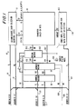
- RAM module 10 can be an embedded array block in a programmable logic device having an architecture such as that described in the above-mentioned Cliff et al. reference, or any other type of device having embedded RAM blocks or modules.
- FIG. 2 shows how a plurality of RAM blocks 10 can be embedded among the logic blocks 21 of programmable logic device 20. Each of logic blocks 21 is made up of several logic modules 22, each of which includes a four-input look-up table. Additional structure of device 20 (including interconnection conductor network 23) can be as shown and described in the above-mentioned Cliff et al. reference.
- Another example of a programmable logic device which can include embedded RAM blocks 10 in accordance with the invention is shown in FIG. 6 and described later in this specification.
- RAM array 11 At the heart of RAM module 10 is the RAM array 11.
- the illustrative RAM module 10 shown in FIG. 1 has one 16-bit write port (DataIn bus conductors 12) and one 16-bit read port (conductors 110).
- RAM array 11 is a two kilobit array arranged as 64 by 32 bits. RAM array 11 can be written by inputting up to 16 bits of data at one time on DataIn bus 12, which feeds column decode, data selection and control logic 13.
- Column control logic 13 uses write address data bits 10 through 6 on AddrW lines 14 to decode and select for which columns of array 11 the data on lines 12 are intended. Thirty-two column select lines 15 and 32 data lines 16 connect column control logic 13 to array 11.
- Additional address data bits 5 through 0, for indicating for which row the data on lines 12 is intended, are input on AddrW lines 17 and are decoded by address decoder 18 and address multiplexer 19.
- address multiplexer 19 passes the decoded address data to array 11 on the addressed one of write enable lines 101.
- elements 18 and 19 operate to select the write enable input 101 for the one of 64 rows of the RAM array that is addressed by AddrW bits 5 through 0.
- row address data bits 5 through 0 are provided on AddrR lines 171 and column address data bits 10 through 6 are provided on AddrR lines 102.
- the column address data on lines 102 control the data output selection logic of output control module 103 to select the columns of RAM array 11 from which data will be output via leads 110.
- the row address data that are input on lines 171 are decoded by address decoder 18 and address multiplexer 19.
- address multiplexer 19 passes the decoded address data to array 11 on the addressed one of 64 read address lines 105.
- field effect transistor 36 connects memory element 31 to data out line 304, which can be read if it is selected by logic 103.
- transistor 36 is turned on by row read line 305, then if element 31 contains a logic "1", transistor 37 pulls data out line 304, held high by pull-up 306, toward ground.
- Reading the output of line 304 may require a sense amplifier, even when RAM module 10 is used as ordinary RAM, and output control logic 103 therefore preferably includes a sense amplifier, which may be conventional, for each output line 304.
- p-term address multiplexer 107 disconnects address lines 205 from address lines 105, and connects them instead to 64 p-term inputs on lines 115, which are the true and complement of the 32 signals on address inputs 14, 102, and 171 and data inputs 12.
- Inputs 12, 14 are available as p-term inputs because they are not normally used in read mode.
- This particular choice of input signals for p-term mode is arbitrary, and instead any other signals could be used for part or all of the 32 p-term mode inputs described in the immediately preceding sentences.
- Lines 205 thus select multiple rows at a time, so that each output line 304 becomes a p-term of the 64 true and complement signals to the extent that in the column associated with that output line the various memory cells are programmed logic "1".
- each line 304 is pulled low if any of the cells 30 on that line is programmed with a logic "1” and is selected by a logic "1" on the associated row read line 305.
- the output on each line 304 is read by a sense amplifier in control logic 103.
- Control logic 103 may also contain one or more OR gates, to each of which two or more of the p-terms on lines 304 can be connected for a sum-of-products output.
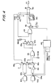
- Logic 103 may also include flip-flops or other register elements to optionally provide registered outputs. An illustrative embodiment of representative portions of logic 103 is shown in more detail in FIG. 4, which will now be described.
- conductors 304n and 304m correspond to two representative instances of conductor 304 in FIG. 3.
- AND gates 402n and 402m represent the AND function performed by the connection of multiple transistors 36 in FIG. 3 to each conductor 304.
- the OR function required for sum-of-products logic is performed by or with the aid of elements 404, 406, 410, 420, 430, and 470.
- the alternate route 440 from conductors 304 to programmable logic connector ("PLC") 450 is used when RAM module 10 is serving as ordinary RAM rather than as p-term logic.
- the circuitry represented by block 440 may therefore be constructed as shown in the above-mentioned Cliff et al. reference. When used to perform sum-of-products logic, the circuitry shown in FIG. 4 may be thought of as logic macrocell circuitry, and it will sometimes be referred to in that way.
- PLC 406a is programmable by FCE R1 to apply either VCC (logic 1) or p-term 304n to one input of PLC 470.
- PLC 406b is programmable by FCE R1 to apply either p-term 304n or VSS (logic 0) to one input of OR gate 410.
- PLC 406c is programmable by FCE R2 to apply either p-term 304m or the logical inverse of p-term 304m (produced by inverter 404) to a second input of OR gate 410.
- the third input to OR gate 410 is a cascade connection 408in from adjacent sum-ofproducts logic (not shown but similar to the logic shown in FIG. 4 for adjacent p-terms 304). In particular, the cascade in 408in of each macrocell is the cascade out 408out of the adjacent macrocell.
- OR gate 410 The output of OR gate 410 is applied to one input terminal of each of PLCs 420a and 420b.
- PLC 420a is programmable by FCE R3 to apply either the output of OR gate 410 or VSS to cascade out 408out.
- PLC 420b is programmable by FCE R3 to apply either the output of OR gate 410 or VSS to one input terminal of EXCLUSIVE OR gate 430.
- the other input to EXCLUSIVE OR gate 430 is the output signal of PLC 470.
- Elements 430 and 470 cooperate to allow the macrocell to produce the EXCLUSIVE OR of the output of OR gate 410 with any of (1) VCC (from PLC 406a), (2) a single p-term 304n output (from PLC 406a), (3) VSS, (4) the Q output of flip-flop 460, or (5) the inverted Q output of flip-flop 460.
- PLC 470 is programmably controlled by FCEs R4 and R5.
- PLC 450 is programmable by FCE 452 (which can be the same as FCE 106 in FIG. 1) to select either the output of EXCLUSIVE OR gate 430 or an output of logic 440 for application to the D input of flip-flop 460 and one input of PLC 480.
- PLC 480 is programmable by FCE R6 to apply either the output of PLC 450 or the Q output of flip-flop 460 to RAM module 10 output lead 110.
- the macrocell shown in FIG. 4 can output either a registered (Q) or combinatorial sum-of-products signal via conductor 110.
- Elements 460 and 480 are usable similarly in conjunction with circuitry 440 to provide either a registered or unregistered conventional RAM or ROM output from RAM module 10.
- the sum-of-products macrocell circuitry shown in FIG. 4 can be generally similar to the macrocell circuitry shown in Pedersen U.S. patent 5,121,006, which is hereby incorporated by reference herein.
- the write port at lines 101 is not used for the above-described p-term mode operation of module 10. Therefore, the write port is available during p-term operation for writing to array 11.
- a device can be provided that is self-modifying, assuming that address data for writing to array 11 can be applied to the array.
- the write address lines are used for p-term inputs, a different arrangement can be used if self-modifying logic is desired. For example, other p-term inputs can be provided in place of using the write address lines that are shown being used for some of those inputs.
- the write address lines can then remain available for use in modifying the contents of array 11. This ability to write into the p-term block (i.e., array 11) can provide effective implementation of logic for reconfigurable computing applications.
- the p-term array 11 can be used as a 32-input 16-output multiplexer, giving flexible routing that can be changed on the fly.
- using the full power of the p-term to implement logic functions allows significantly different logic functions to be "downloaded" by changing the contents of array 11.
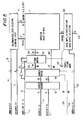
- FIG. 5 shows an example of how the circuitry of FIG. 1 can be modified to facilitate writing new data to array 11 to allow complete freedom to change the data in array 11 without interfering with use of the array as a p-term array in sum-of-products logic.
- the 32 word line signals needed by array 11 in p-term mode come from separate word line signal conductors 114, rather than being "borrowed” from other sources like conductors 12, 14, 102, and 171. (Such independent sourcing of all the word line signals is not absolutely necessary. For example, some of the word line signals could still be "borrowed" as in FIG.
- circuitry shown in FIG. 5 has all the additional advantageous characteristics described in the immediately preceding paragraph (e.g., the circuitry can implement logic for reconfigurable computing applications, the circuitry can function as a dynamic 32-input 16-output multiplexer, and significantly different p-term logic functions can be "downloaded" into array 11 whenever desired).
- RAM blocks 10 of an SRAM-based look-up-table-type device 20 By configuring RAM blocks 10 of an SRAM-based look-up-table-type device 20 in the manner shown herein, one obtains a look-up-table-type device that can optionally provide p-term logic functions of large numbers of inputs.
- FIG. 6 shows another example of a programmable logic device 20' having RAM blocks 10 embedded among logic blocks 21'.
- device 20' may be constructed generally as shown in Freeman United States patent Re. 34,363, which is also hereby incorporated by reference herein.
- each logic block 21' may be a configurable logic block ("CLB") which includes one or two small look-up tables.
- CLB 21' may be surrounded by interconnection conductors 23' for conveying signals to, from, and between CLBs 21' and other circuitry on or off the device.
- Such other circuitry on the device includes RAM blocks 10.
- Each CLB 21' may receive signals from the interconnection conductors 23' adjacent to any of its sides.
- each CLB may output signals to any of its sides.
- each RAM block 10 is usable either as ordinary RAM/ROM or to perform p-term logic.
- FIG. 7 illustrates a programmable logic device 20/20' of this invention in a data processing system 502.
- Data processing system 502 may include one or more of the following components: a processor 504; memory 506; I/O circuitry 508; and peripheral devices 510. These components are coupled together by a system bus 520 and are populated on a circuit board 530 which is contained in an end-user system 540.
- System 502 can be used in a wide variety of applications, such as computer networking, data networking, instrumentation, video processing, digital signal processing, or any other application where the advantage of using programmable or reprogrammable logic is desirable.
- Programmable logic device 20/20' can be used to perform a variety of different logic functions.
- programmable logic device 20/20' can be configured as a processor or controller that works in cooperation with processor 504.
- Programmable logic device 20/20' may also be used as an arbiter for arbitrating access to a shared resource in system 502.
- programmable logic device 20/20' can be configured as an interface between processor 504 and one of the other components in system 502. It should be noted that system 502 is only exemplary, and that the true scope and spirit of the invention should be indicated by the following claims.
- function control elements 106 and other FCEs can be SRAMs, DRAMs, first-in first-out ("FIFO") memories, EPROMs, EEPROMs, function control registers (e.g., as in Wahlstrom U.S. patent 3,473,160), ferro-electric memories, fuses, antifuses, or the like. From the various examples mentioned above it will be seen that this invention is applicable to both one-time-only programmable and reprogrammable devices.
- each transistor 37 could be logic 1 1 rather than logic 0 as shown in FIG. 3, and each data out conductor 304 could have a pull down connection to logic 0 rather than a pull up connection to logic 1 as shown in FIG. 3.
Landscapes
- Physics & Mathematics (AREA)
- Mathematical Physics (AREA)
- Engineering & Computer Science (AREA)
- Computer Hardware Design (AREA)
- Computing Systems (AREA)
- General Engineering & Computer Science (AREA)
- Logic Circuits (AREA)
Applications Claiming Priority (4)
| Application Number | Priority Date | Filing Date | Title |
|---|---|---|---|
| US4104697P | 1997-03-21 | 1997-03-21 | |
| US41046P | 1997-03-21 | ||
| US09/034,050 US6020759A (en) | 1997-03-21 | 1998-03-03 | Programmable logic array device with random access memory configurable as product terms |
| US34050P | 1998-03-03 |
Publications (2)
| Publication Number | Publication Date |
|---|---|
| EP0866558A2 true EP0866558A2 (de) | 1998-09-23 |
| EP0866558A3 EP0866558A3 (de) | 1999-12-08 |
Family
ID=26710485
Family Applications (1)
| Application Number | Title | Priority Date | Filing Date |
|---|---|---|---|
| EP98302057A Withdrawn EP0866558A3 (de) | 1997-03-21 | 1998-03-18 | Programmbares logisches Feld mit als Produktterm konfigurierbarem Speicher mit wahlfreiem Zugriff |
Country Status (3)
| Country | Link |
|---|---|
| US (4) | US6020759A (de) |
| EP (1) | EP0866558A3 (de) |
| JP (1) | JPH11243334A (de) |
Cited By (2)
| Publication number | Priority date | Publication date | Assignee | Title |
|---|---|---|---|---|
| EP1177631A4 (de) * | 1999-05-07 | 2002-07-03 | Morphics Tech Inc | Heterogenes programmierbares gatterfeld |
| GB2387003A (en) * | 2002-02-11 | 2003-10-01 | Lattice Semiconductor Corp | Programmable device with generic logic blocks for perfoming logic and/or memory functions |
Families Citing this family (96)
| Publication number | Priority date | Publication date | Assignee | Title |
|---|---|---|---|---|
| US6020759A (en) | 1997-03-21 | 2000-02-01 | Altera Corporation | Programmable logic array device with random access memory configurable as product terms |
| US6128215A (en) * | 1997-08-19 | 2000-10-03 | Altera Corporation | Static random access memory circuits |
| US6104208A (en) * | 1998-03-04 | 2000-08-15 | Altera Corporation | Programmable logic device incorporating function blocks operable as wide-shallow RAM |
| US6467017B1 (en) * | 1998-06-23 | 2002-10-15 | Altera Corporation | Programmable logic device having embedded dual-port random access memory configurable as single-port memory |
| US6144573A (en) * | 1998-06-26 | 2000-11-07 | Altera Corporation | Programmable logic devices with improved content addressable memory capabilities |
| US6433579B1 (en) * | 1998-07-02 | 2002-08-13 | Altera Corporation | Programmable logic integrated circuit devices with differential signaling capabilities |
| US6215326B1 (en) * | 1998-11-18 | 2001-04-10 | Altera Corporation | Programmable logic device architecture with super-regions having logic regions and a memory region |
| US6225822B1 (en) | 1998-11-18 | 2001-05-01 | Altera Corporation | Fast signal conductor networks for programmable logic devices |
| US6326808B1 (en) * | 1998-12-03 | 2001-12-04 | Vantis Corporation | Inversion of product term line before or logic in a programmable logic device (PLD) |
| US6472903B1 (en) * | 1999-01-08 | 2002-10-29 | Altera Corporation | Programmable logic device input/output architecture with power bus segmentation for multiple I/O standards |
| US6603332B2 (en) | 1999-02-25 | 2003-08-05 | Xilinx, Inc. | Configurable logic block for PLD with logic gate for combining output with another configurable logic block |
| US6396302B2 (en) * | 1999-02-25 | 2002-05-28 | Xilinx, Inc. | Configurable logic element with expander structures |
| US6184712B1 (en) | 1999-02-25 | 2001-02-06 | Xilinx, Inc. | FPGA configurable logic block with multi-purpose logic/memory circuit |
| US6400180B2 (en) | 1999-02-25 | 2002-06-04 | Xilinix, Inc. | Configurable lookup table for programmable logic devices |
| US6150838A (en) * | 1999-02-25 | 2000-11-21 | Xilinx, Inc. | FPGA configurable logic block with multi-purpose logic/memory circuit |
| US6407576B1 (en) * | 1999-03-04 | 2002-06-18 | Altera Corporation | Interconnection and input/output resources for programmable logic integrated circuit devices |
| AU1727901A (en) * | 1999-11-29 | 2001-06-04 | Cellot Inc. | Universal hardware device and method and tools for use therewith |
| US7185293B1 (en) | 1999-11-29 | 2007-02-27 | Cellot, Inc. | Universal hardware device and method and tools for use therewith |
| US6256253B1 (en) * | 2000-02-18 | 2001-07-03 | Infineon Technologies North America Corp. | Memory device with support for unaligned access |
| US6400635B1 (en) | 2000-03-15 | 2002-06-04 | Altera Corporation | Memory circuitry for programmable logic integrated circuit devices |
| US6661733B1 (en) * | 2000-06-15 | 2003-12-09 | Altera Corporation | Dual-port SRAM in a programmable logic device |
| US7119576B1 (en) | 2000-09-18 | 2006-10-10 | Altera Corporation | Devices and methods with programmable logic and digital signal processing regions |
| US7346644B1 (en) | 2000-09-18 | 2008-03-18 | Altera Corporation | Devices and methods with programmable logic and digital signal processing regions |
| US6754766B1 (en) | 2002-02-14 | 2004-06-22 | Altera Corporation | Emulation of content-addressable memories |
| US6747480B1 (en) | 2002-07-12 | 2004-06-08 | Altera Corporation | Programmable logic devices with bidirect ional cascades |
| US7111110B1 (en) | 2002-12-10 | 2006-09-19 | Altera Corporation | Versatile RAM for programmable logic device |
| US6888372B1 (en) * | 2002-12-20 | 2005-05-03 | Altera Corporation | Programmable logic device with soft multiplier |
| JP3958232B2 (ja) | 2003-03-05 | 2007-08-15 | 富士通株式会社 | 動作継続中にデータ書き換え可能な論理装置 |
| US6894531B1 (en) * | 2003-05-22 | 2005-05-17 | Altera Corporation | Interface for a programmable logic device |
| KR100610006B1 (ko) * | 2004-05-04 | 2006-08-08 | 삼성전자주식회사 | 호스트 시스템의 다중동작 지원에 적합한 메모리 구조를갖는 반도체 메모리 장치 |
| US7218141B2 (en) * | 2004-12-07 | 2007-05-15 | Altera Corporation | Techniques for implementing hardwired decoders in differential input circuits |
| WO2007015479A1 (ja) * | 2005-08-01 | 2007-02-08 | Matsushita Electric Industrial Co., Ltd. | プログラマブル・ロジック・アレイ及びプログラマブル・ロジック・アレイモジュールジェネレータ |
| US8620980B1 (en) | 2005-09-27 | 2013-12-31 | Altera Corporation | Programmable device with specialized multiplier blocks |
| US8266199B2 (en) * | 2006-02-09 | 2012-09-11 | Altera Corporation | Specialized processing block for programmable logic device |
| US8266198B2 (en) * | 2006-02-09 | 2012-09-11 | Altera Corporation | Specialized processing block for programmable logic device |
| US8041759B1 (en) | 2006-02-09 | 2011-10-18 | Altera Corporation | Specialized processing block for programmable logic device |
| US8301681B1 (en) | 2006-02-09 | 2012-10-30 | Altera Corporation | Specialized processing block for programmable logic device |
| US7836117B1 (en) | 2006-04-07 | 2010-11-16 | Altera Corporation | Specialized processing block for programmable logic device |
| US7822799B1 (en) | 2006-06-26 | 2010-10-26 | Altera Corporation | Adder-rounder circuitry for specialized processing block in programmable logic device |
| US8386550B1 (en) | 2006-09-20 | 2013-02-26 | Altera Corporation | Method for configuring a finite impulse response filter in a programmable logic device |
| JP4191219B2 (ja) * | 2006-10-30 | 2008-12-03 | エルピーダメモリ株式会社 | メモリ回路、半導体装置及びメモリ回路の制御方法 |
| US7930336B2 (en) * | 2006-12-05 | 2011-04-19 | Altera Corporation | Large multiplier for programmable logic device |
| US8386553B1 (en) | 2006-12-05 | 2013-02-26 | Altera Corporation | Large multiplier for programmable logic device |
| US7814137B1 (en) | 2007-01-09 | 2010-10-12 | Altera Corporation | Combined interpolation and decimation filter for programmable logic device |
| US8650231B1 (en) | 2007-01-22 | 2014-02-11 | Altera Corporation | Configuring floating point operations in a programmable device |
| US7865541B1 (en) | 2007-01-22 | 2011-01-04 | Altera Corporation | Configuring floating point operations in a programmable logic device |
| US8645450B1 (en) | 2007-03-02 | 2014-02-04 | Altera Corporation | Multiplier-accumulator circuitry and methods |
| US7949699B1 (en) | 2007-08-30 | 2011-05-24 | Altera Corporation | Implementation of decimation filter in integrated circuit device using ram-based data storage |
| JP5260077B2 (ja) * | 2008-02-15 | 2013-08-14 | 太陽誘電株式会社 | プログラマブル論理デバイスおよびその構築方法およびその使用方法 |
| US8959137B1 (en) | 2008-02-20 | 2015-02-17 | Altera Corporation | Implementing large multipliers in a programmable integrated circuit device |
| US8244789B1 (en) | 2008-03-14 | 2012-08-14 | Altera Corporation | Normalization of floating point operations in a programmable integrated circuit device |
| US8626815B1 (en) | 2008-07-14 | 2014-01-07 | Altera Corporation | Configuring a programmable integrated circuit device to perform matrix multiplication |
| US8255448B1 (en) | 2008-10-02 | 2012-08-28 | Altera Corporation | Implementing division in a programmable integrated circuit device |
| US8307023B1 (en) | 2008-10-10 | 2012-11-06 | Altera Corporation | DSP block for implementing large multiplier on a programmable integrated circuit device |
| US8468192B1 (en) | 2009-03-03 | 2013-06-18 | Altera Corporation | Implementing multipliers in a programmable integrated circuit device |
| US8645449B1 (en) | 2009-03-03 | 2014-02-04 | Altera Corporation | Combined floating point adder and subtractor |
| US8886696B1 (en) | 2009-03-03 | 2014-11-11 | Altera Corporation | Digital signal processing circuitry with redundancy and ability to support larger multipliers |
| US8706790B1 (en) | 2009-03-03 | 2014-04-22 | Altera Corporation | Implementing mixed-precision floating-point operations in a programmable integrated circuit device |
| US8805916B2 (en) * | 2009-03-03 | 2014-08-12 | Altera Corporation | Digital signal processing circuitry with redundancy and bidirectional data paths |
| US8549055B2 (en) * | 2009-03-03 | 2013-10-01 | Altera Corporation | Modular digital signal processing circuitry with optionally usable, dedicated connections between modules of the circuitry |
| US8650236B1 (en) | 2009-08-04 | 2014-02-11 | Altera Corporation | High-rate interpolation or decimation filter in integrated circuit device |
| US8396914B1 (en) | 2009-09-11 | 2013-03-12 | Altera Corporation | Matrix decomposition in an integrated circuit device |
| US8412756B1 (en) | 2009-09-11 | 2013-04-02 | Altera Corporation | Multi-operand floating point operations in a programmable integrated circuit device |
| US8539016B1 (en) | 2010-02-09 | 2013-09-17 | Altera Corporation | QR decomposition in an integrated circuit device |
| US7948267B1 (en) | 2010-02-09 | 2011-05-24 | Altera Corporation | Efficient rounding circuits and methods in configurable integrated circuit devices |
| US8601044B2 (en) * | 2010-03-02 | 2013-12-03 | Altera Corporation | Discrete Fourier Transform in an integrated circuit device |
| US8458243B1 (en) | 2010-03-03 | 2013-06-04 | Altera Corporation | Digital signal processing circuit blocks with support for systolic finite-impulse-response digital filtering |
| US8484265B1 (en) | 2010-03-04 | 2013-07-09 | Altera Corporation | Angular range reduction in an integrated circuit device |
| US8510354B1 (en) | 2010-03-12 | 2013-08-13 | Altera Corporation | Calculation of trigonometric functions in an integrated circuit device |
| US8539014B2 (en) * | 2010-03-25 | 2013-09-17 | Altera Corporation | Solving linear matrices in an integrated circuit device |
| US8589463B2 (en) | 2010-06-25 | 2013-11-19 | Altera Corporation | Calculation of trigonometric functions in an integrated circuit device |
| US8862650B2 (en) | 2010-06-25 | 2014-10-14 | Altera Corporation | Calculation of trigonometric functions in an integrated circuit device |
| US8577951B1 (en) | 2010-08-19 | 2013-11-05 | Altera Corporation | Matrix operations in an integrated circuit device |
| US8400863B1 (en) * | 2010-08-20 | 2013-03-19 | Altera Corporation | Configurable memory block |
| US8645451B2 (en) | 2011-03-10 | 2014-02-04 | Altera Corporation | Double-clocked specialized processing block in an integrated circuit device |
| US9600278B1 (en) | 2011-05-09 | 2017-03-21 | Altera Corporation | Programmable device using fixed and configurable logic to implement recursive trees |
| US8812576B1 (en) | 2011-09-12 | 2014-08-19 | Altera Corporation | QR decomposition in an integrated circuit device |
| US8949298B1 (en) | 2011-09-16 | 2015-02-03 | Altera Corporation | Computing floating-point polynomials in an integrated circuit device |
| US9053045B1 (en) | 2011-09-16 | 2015-06-09 | Altera Corporation | Computing floating-point polynomials in an integrated circuit device |
| US8868820B2 (en) * | 2011-10-31 | 2014-10-21 | Microsemi SoC Corporation | RAM block designed for efficient ganging |
| US8762443B1 (en) | 2011-11-15 | 2014-06-24 | Altera Corporation | Matrix operations in an integrated circuit device |
| TWI455485B (zh) * | 2012-02-22 | 2014-10-01 | Global Unichip Corp | 由數位電路與類比電路所共用之輸入輸出單元 |
| US9965208B1 (en) | 2012-02-23 | 2018-05-08 | Micron Technology, Inc. | Memory device having a controller to enable and disable mode control circuitry of the controller |
| US8543634B1 (en) | 2012-03-30 | 2013-09-24 | Altera Corporation | Specialized processing block for programmable integrated circuit device |
| US9098332B1 (en) | 2012-06-01 | 2015-08-04 | Altera Corporation | Specialized processing block with fixed- and floating-point structures |
| US8996600B1 (en) | 2012-08-03 | 2015-03-31 | Altera Corporation | Specialized processing block for implementing floating-point multiplier with subnormal operation support |
| US9207909B1 (en) | 2012-11-26 | 2015-12-08 | Altera Corporation | Polynomial calculations optimized for programmable integrated circuit device structures |
| US9189200B1 (en) | 2013-03-14 | 2015-11-17 | Altera Corporation | Multiple-precision processing block in a programmable integrated circuit device |
| US9348795B1 (en) | 2013-07-03 | 2016-05-24 | Altera Corporation | Programmable device using fixed and configurable logic to implement floating-point rounding |
| US9983990B1 (en) | 2013-11-21 | 2018-05-29 | Altera Corporation | Configurable storage circuits with embedded processing and control circuitry |
| US9379687B1 (en) | 2014-01-14 | 2016-06-28 | Altera Corporation | Pipelined systolic finite impulse response filter |
| US9954533B2 (en) * | 2014-12-16 | 2018-04-24 | Samsung Electronics Co., Ltd. | DRAM-based reconfigurable logic |
| US9880952B2 (en) | 2015-01-15 | 2018-01-30 | Toshiba Memory Corporation | Bus access controller, hardware engine, controller, and memory system |
| US9684488B2 (en) | 2015-03-26 | 2017-06-20 | Altera Corporation | Combined adder and pre-adder for high-radix multiplier circuit |
| US9779785B2 (en) | 2015-05-11 | 2017-10-03 | Wisconsin Alumni Research Foundation | Computer architecture using compute/storage tiles |
| US10942706B2 (en) | 2017-05-05 | 2021-03-09 | Intel Corporation | Implementation of floating-point trigonometric functions in an integrated circuit device |
Family Cites Families (36)
| Publication number | Priority date | Publication date | Assignee | Title |
|---|---|---|---|---|
| US34363A (en) * | 1862-02-11 | Improvement in machinery for cleaning cotton | ||
| US3473160A (en) * | 1966-10-10 | 1969-10-14 | Stanford Research Inst | Electronically controlled microelectronic cellular logic array |
| US3849638A (en) * | 1973-07-18 | 1974-11-19 | Gen Electric | Segmented associative logic circuits |
| US4195352A (en) * | 1977-07-08 | 1980-03-25 | Xerox Corporation | Split programmable logic array |
| USRE34363E (en) | 1984-03-12 | 1993-08-31 | Xilinx, Inc. | Configurable electrical circuit having configurable logic elements and configurable interconnects |
| DE3477622D1 (en) * | 1984-11-30 | 1989-05-11 | Ibm | Memory using conventional cells to perform a ram or an associative memory function |
| JP2541248B2 (ja) * | 1987-11-20 | 1996-10-09 | 三菱電機株式会社 | プログラマブル・ロジック・アレイ |
| US4912345A (en) * | 1988-12-29 | 1990-03-27 | Sgs-Thomson Microelectronics, Inc. | Programmable summing functions for programmable logic devices |
| US5099150A (en) * | 1989-09-29 | 1992-03-24 | Sgs-Thomson Microelectronics, Inc. | Circuit block for programmable logic devices, configurable as a user-writable memory or a logic circuit |
| US5128559A (en) * | 1989-09-29 | 1992-07-07 | Sgs-Thomson Microelectronics, Inc. | Logic block for programmable logic devices |
| US4975601A (en) * | 1989-09-29 | 1990-12-04 | Sgs-Thomson Microelectronics, Inc. | User-writable random access memory logic block for programmable logic devices |
| US5027011A (en) * | 1989-10-31 | 1991-06-25 | Sgs-Thomson Microelectronics, Inc. | Input row drivers for programmable logic devices |
| US5144582A (en) * | 1990-03-30 | 1992-09-01 | Sgs-Thomson Microelectronics, Inc. | Sram based cell for programmable logic devices |
| US5121006A (en) * | 1991-04-22 | 1992-06-09 | Altera Corporation | Registered logic macrocell with product term allocation and adjacent product term stealing |
| US5883850A (en) * | 1991-09-03 | 1999-03-16 | Altera Corporation | Programmable logic array integrated circuits |
| US5633830A (en) * | 1995-11-08 | 1997-05-27 | Altera Corporation | Random access memory block circuitry for programmable logic array integrated circuit devices |
| US5550782A (en) * | 1991-09-03 | 1996-08-27 | Altera Corporation | Programmable logic array integrated circuits |
| US5270587A (en) * | 1992-01-06 | 1993-12-14 | Micron Technology, Inc. | CMOS logic cell for high-speed, zero-power programmable array logic devices |
| US5383146A (en) * | 1992-06-08 | 1995-01-17 | Music Semiconductors, Inc. | Memory with CAM and RAM partitions |
| GB9303084D0 (en) * | 1993-02-16 | 1993-03-31 | Inmos Ltd | Programmable logic circuit |
| US5302865A (en) * | 1993-02-16 | 1994-04-12 | Intel Corporation | High-speed comparator logic for wide compares in programmable logic devices |
| US5362999A (en) * | 1993-03-18 | 1994-11-08 | Xilinx, Inc. | EPLD chip with hybrid architecture optimized for both speed and flexibility |
| US5809281A (en) * | 1993-03-30 | 1998-09-15 | Altera Corporation | Field programmable gate array with high speed SRAM based configurable function block configurable as high performance logic or block of SRAM |
| US5386155A (en) * | 1993-03-30 | 1995-01-31 | Intel Corporation | Apparatus and method for selecting polarity and output type in a programmable logic device |
| US5450608A (en) * | 1993-04-15 | 1995-09-12 | Intel Corporation | Programmable logic having selectable output states for initialization and resets asynchronously using control bit associated with each product term |
| US5689195A (en) * | 1995-05-17 | 1997-11-18 | Altera Corporation | Programmable logic array integrated circuit devices |
| KR0120579B1 (ko) * | 1994-07-14 | 1997-10-30 | 김주용 | 리 프로그램가능한 프로그램어블 로직 어래이 |
| JPH0863975A (ja) * | 1994-08-25 | 1996-03-08 | Fujitsu Ltd | スタティックramおよびこのスタティックramを有する処理装置 |
| US5761099A (en) * | 1994-11-04 | 1998-06-02 | Altera Corporation | Programmable logic array integrated circuits with enhanced carry routing |
| US5532957A (en) * | 1995-01-31 | 1996-07-02 | Texas Instruments Incorporated | Field reconfigurable logic/memory array |
| US6049223A (en) * | 1995-03-22 | 2000-04-11 | Altera Corporation | Programmable logic array integrated circuit with general-purpose memory configurable as a random access or FIFO memory |
| US5757207A (en) * | 1995-03-22 | 1998-05-26 | Altera Corporation | Programmable logic array integrated circuit incorporating a first-in first-out memory |
| US5559450A (en) * | 1995-07-27 | 1996-09-24 | Lucent Technologies Inc. | Field programmable gate array with multi-port RAM |
| US5744980A (en) * | 1996-02-16 | 1998-04-28 | Actel Corporation | Flexible, high-performance static RAM architecture for field-programmable gate arrays |
| US6020759A (en) * | 1997-03-21 | 2000-02-01 | Altera Corporation | Programmable logic array device with random access memory configurable as product terms |
| US6052327A (en) * | 1997-10-14 | 2000-04-18 | Altera Corporation | Dual-port programmable logic device variable depth and width memory array |
-
1998
- 1998-03-03 US US09/034,050 patent/US6020759A/en not_active Expired - Lifetime
- 1998-03-18 EP EP98302057A patent/EP0866558A3/de not_active Withdrawn
- 1998-03-21 JP JP10092511A patent/JPH11243334A/ja active Pending
-
1999
- 1999-11-19 US US09/443,970 patent/US6118720A/en not_active Expired - Fee Related
-
2000
- 2000-06-22 US US09/599,764 patent/US6347061B1/en not_active Expired - Lifetime
-
2001
- 2001-12-26 US US10/033,976 patent/US6556500B2/en not_active Expired - Fee Related
Cited By (6)
| Publication number | Priority date | Publication date | Assignee | Title |
|---|---|---|---|---|
| EP1177631A4 (de) * | 1999-05-07 | 2002-07-03 | Morphics Tech Inc | Heterogenes programmierbares gatterfeld |
| GB2387003A (en) * | 2002-02-11 | 2003-10-01 | Lattice Semiconductor Corp | Programmable device with generic logic blocks for perfoming logic and/or memory functions |
| GB2387003B (en) * | 2002-02-11 | 2004-04-21 | Lattice Semiconductor Corp | Device and method with generic logic blocks |
| US6765408B2 (en) | 2002-02-11 | 2004-07-20 | Lattice Semiconductor Corporation | Device and method with generic logic blocks |
| US6903573B1 (en) | 2002-02-11 | 2005-06-07 | Lattice Semiconductor Corporation | Programmable logic device with enhanced wide input product term cascading |
| US6915323B1 (en) | 2002-02-11 | 2005-07-05 | Lattice Semiconductor Corporation | Macrocells supporting a carry cascade |
Also Published As
| Publication number | Publication date |
|---|---|
| JPH11243334A (ja) | 1999-09-07 |
| US6118720A (en) | 2000-09-12 |
| US6020759A (en) | 2000-02-01 |
| EP0866558A3 (de) | 1999-12-08 |
| US20020057621A1 (en) | 2002-05-16 |
| US6347061B1 (en) | 2002-02-12 |
| US6556500B2 (en) | 2003-04-29 |
Similar Documents
| Publication | Publication Date | Title |
|---|---|---|
| US6020759A (en) | Programmable logic array device with random access memory configurable as product terms | |
| US6191611B1 (en) | Driver circuitry for programmable logic devices with hierarchical interconnection resources | |
| US5850152A (en) | Programmable logic array integrated circuit devices | |
| US6501296B2 (en) | Logic/memory circuit having a plurality of operating modes | |
| US6184712B1 (en) | FPGA configurable logic block with multi-purpose logic/memory circuit | |
| US5986465A (en) | Programmable logic integrated circuit architecture incorporating a global shareable expander | |
| US6467017B1 (en) | Programmable logic device having embedded dual-port random access memory configurable as single-port memory | |
| US5898318A (en) | Programmable logic array integrated circuits with enhanced cascade | |
| US5371422A (en) | Programmable logic device having multiplexers and demultiplexers randomly connected to global conductors for interconnections between logic elements | |
| US6215326B1 (en) | Programmable logic device architecture with super-regions having logic regions and a memory region | |
| EP0746103B1 (de) | Integrierte Schaltungen mit programmierbaren logischen Feldern | |
| US6034540A (en) | Programmable logic integrated circuit architecture incorporating a lonely register | |
| US6812738B1 (en) | Vector routing in a programmable logic device | |
| US6747480B1 (en) | Programmable logic devices with bidirect ional cascades | |
| GB2318198A (en) | Programmable logic | |
| US6344989B1 (en) | Programmable logic devices with improved content addressable memory capabilities | |
| GB2318663A (en) | Hierarchical interconnect for programmable logic devices | |
| US6356110B1 (en) | Multifunction memory array in a programmable logic device | |
| US6072332A (en) | Variable depth memories for programmable logic devices | |
| US6278288B1 (en) | Programmable logic device with enhanced multiplexing capabilities in interconnect resources | |
| US6263482B1 (en) | Programmable logic device having macrocells with selectable product-term inversion | |
| US5936425A (en) | Tri-statable input/output circuitry for programmable logic | |
| US6819135B2 (en) | Fast signal conductor networks for programmable logic devices | |
| GB2333872A (en) | Programmable logic array |
Legal Events
| Date | Code | Title | Description |
|---|---|---|---|
| PUAI | Public reference made under article 153(3) epc to a published international application that has entered the european phase |
Free format text: ORIGINAL CODE: 0009012 |
|
| AK | Designated contracting states |
Kind code of ref document: A2 Designated state(s): DE FR GB IT NL |
|
| AX | Request for extension of the european patent |
Free format text: AL;LT;LV;MK;RO;SI |
|
| PUAL | Search report despatched |
Free format text: ORIGINAL CODE: 0009013 |
|
| AK | Designated contracting states |
Kind code of ref document: A3 Designated state(s): AT BE CH DE DK ES FI FR GB GR IE IT LI LU MC NL PT SE |
|
| AX | Request for extension of the european patent |
Free format text: AL;LT;LV;MK;RO;SI |
|
| RIC1 | Information provided on ipc code assigned before grant |
Free format text: 6H 03K 19/177 A, 6H 03K 19/173 B |
|
| 17P | Request for examination filed |
Effective date: 20000505 |
|
| AKX | Designation fees paid |
Free format text: DE FR GB IT NL |
|
| 17Q | First examination report despatched |
Effective date: 20040616 |
|
| STAA | Information on the status of an ep patent application or granted ep patent |
Free format text: STATUS: THE APPLICATION IS DEEMED TO BE WITHDRAWN |
|
| 18D | Application deemed to be withdrawn |
Effective date: 20041228 |