EP0867014B1 - Carte a puce - Google Patents
Carte a puce Download PDFInfo
- Publication number
- EP0867014B1 EP0867014B1 EP96946372A EP96946372A EP0867014B1 EP 0867014 B1 EP0867014 B1 EP 0867014B1 EP 96946372 A EP96946372 A EP 96946372A EP 96946372 A EP96946372 A EP 96946372A EP 0867014 B1 EP0867014 B1 EP 0867014B1
- Authority
- EP
- European Patent Office
- Prior art keywords
- chip
- memory
- card
- processor
- mirror
- Prior art date
- Legal status (The legal status is an assumption and is not a legal conclusion. Google has not performed a legal analysis and makes no representation as to the accuracy of the status listed.)
- Expired - Lifetime
Links
Images
Classifications
-
- G—PHYSICS
- G07—CHECKING-DEVICES
- G07F—COIN-FREED OR LIKE APPARATUS
- G07F7/00—Mechanisms actuated by objects other than coins to free or to actuate vending, hiring, coin or paper currency dispensing or refunding apparatus
- G07F7/08—Mechanisms actuated by objects other than coins to free or to actuate vending, hiring, coin or paper currency dispensing or refunding apparatus by coded identity card or credit card or other personal identification means
- G07F7/10—Mechanisms actuated by objects other than coins to free or to actuate vending, hiring, coin or paper currency dispensing or refunding apparatus by coded identity card or credit card or other personal identification means together with a coded signal, e.g. in the form of personal identification information, like personal identification number [PIN] or biometric data
- G07F7/1008—Active credit-cards provided with means to personalise their use, e.g. with PIN-introduction/comparison system
-
- G—PHYSICS
- G06—COMPUTING OR CALCULATING; COUNTING
- G06K—GRAPHICAL DATA READING; PRESENTATION OF DATA; RECORD CARRIERS; HANDLING RECORD CARRIERS
- G06K19/00—Record carriers for use with machines and with at least a part designed to carry digital markings
- G06K19/06—Record carriers for use with machines and with at least a part designed to carry digital markings characterised by the kind of the digital marking, e.g. shape, nature, code
- G06K19/067—Record carriers with conductive marks, printed circuits or semiconductor circuit elements, e.g. credit or identity cards also with resonating or responding marks without active components
- G06K19/07—Record carriers with conductive marks, printed circuits or semiconductor circuit elements, e.g. credit or identity cards also with resonating or responding marks without active components with integrated circuit chips
-
- G—PHYSICS
- G06—COMPUTING OR CALCULATING; COUNTING
- G06K—GRAPHICAL DATA READING; PRESENTATION OF DATA; RECORD CARRIERS; HANDLING RECORD CARRIERS
- G06K19/00—Record carriers for use with machines and with at least a part designed to carry digital markings
- G06K19/06—Record carriers for use with machines and with at least a part designed to carry digital markings characterised by the kind of the digital marking, e.g. shape, nature, code
- G06K19/067—Record carriers with conductive marks, printed circuits or semiconductor circuit elements, e.g. credit or identity cards also with resonating or responding marks without active components
- G06K19/07—Record carriers with conductive marks, printed circuits or semiconductor circuit elements, e.g. credit or identity cards also with resonating or responding marks without active components with integrated circuit chips
- G06K19/0701—Record carriers with conductive marks, printed circuits or semiconductor circuit elements, e.g. credit or identity cards also with resonating or responding marks without active components with integrated circuit chips at least one of the integrated circuit chips comprising an arrangement for power management
- G06K19/0702—Record carriers with conductive marks, printed circuits or semiconductor circuit elements, e.g. credit or identity cards also with resonating or responding marks without active components with integrated circuit chips at least one of the integrated circuit chips comprising an arrangement for power management the arrangement including a battery
- G06K19/0704—Record carriers with conductive marks, printed circuits or semiconductor circuit elements, e.g. credit or identity cards also with resonating or responding marks without active components with integrated circuit chips at least one of the integrated circuit chips comprising an arrangement for power management the arrangement including a battery the battery being rechargeable, e.g. solar batteries
-
- G—PHYSICS
- G06—COMPUTING OR CALCULATING; COUNTING
- G06K—GRAPHICAL DATA READING; PRESENTATION OF DATA; RECORD CARRIERS; HANDLING RECORD CARRIERS
- G06K19/00—Record carriers for use with machines and with at least a part designed to carry digital markings
- G06K19/06—Record carriers for use with machines and with at least a part designed to carry digital markings characterised by the kind of the digital marking, e.g. shape, nature, code
- G06K19/067—Record carriers with conductive marks, printed circuits or semiconductor circuit elements, e.g. credit or identity cards also with resonating or responding marks without active components
- G06K19/07—Record carriers with conductive marks, printed circuits or semiconductor circuit elements, e.g. credit or identity cards also with resonating or responding marks without active components with integrated circuit chips
- G06K19/077—Constructional details, e.g. mounting of circuits in the carrier
- G06K19/07701—Constructional details, e.g. mounting of circuits in the carrier the record carrier comprising an interface suitable for human interaction
- G06K19/07703—Constructional details, e.g. mounting of circuits in the carrier the record carrier comprising an interface suitable for human interaction the interface being visual
-
- G—PHYSICS
- G06—COMPUTING OR CALCULATING; COUNTING
- G06Q—INFORMATION AND COMMUNICATION TECHNOLOGY [ICT] SPECIALLY ADAPTED FOR ADMINISTRATIVE, COMMERCIAL, FINANCIAL, MANAGERIAL OR SUPERVISORY PURPOSES; SYSTEMS OR METHODS SPECIALLY ADAPTED FOR ADMINISTRATIVE, COMMERCIAL, FINANCIAL, MANAGERIAL OR SUPERVISORY PURPOSES, NOT OTHERWISE PROVIDED FOR
- G06Q20/00—Payment architectures, schemes or protocols
- G06Q20/30—Payment architectures, schemes or protocols characterised by the use of specific devices or networks
- G06Q20/34—Payment architectures, schemes or protocols characterised by the use of specific devices or networks using cards, e.g. integrated circuit [IC] cards or magnetic cards
- G06Q20/341—Active cards, i.e. cards including their own processing means, e.g. including an IC or chip
-
- G—PHYSICS
- G07—CHECKING-DEVICES
- G07F—COIN-FREED OR LIKE APPARATUS
- G07F7/00—Mechanisms actuated by objects other than coins to free or to actuate vending, hiring, coin or paper currency dispensing or refunding apparatus
- G07F7/08—Mechanisms actuated by objects other than coins to free or to actuate vending, hiring, coin or paper currency dispensing or refunding apparatus by coded identity card or credit card or other personal identification means
- G07F7/0806—Details of the card
- G07F7/0813—Specific details related to card security
- G07F7/082—Features insuring the integrity of the data on or in the card
Definitions
- the invention is directed to a chip card comprising a memory chip and / or processor chip.
- chip cards are increasingly used in cashless payments through because it's about pure detection and storage, such as with the help of a magnetic stripe, an interactive communication with an external reader or writer. Accordingly, information can be read from the chip card in the smart card new information registered and interacting information is processed with the chip card, for example for Generation of an identifier in the manner of a signature or an access authorization enabling key.
- the communication between card and reader or writer can either done by the card having a contact field and with corresponded contacts of the reader-writer in contact is, or contactless, for example by inductive or capacitive information transfer.
- a major disadvantage of known chip cards is that they can also be used essentially limited is that the information content the cards can only be read in conjunction with a reader / writer can be. In other words, the regulation requires that the cardholder inserts his card into or with such a device communicates without contact, and then saved on the device on the card Being able to read out information.
- EP 0 534 559 A1 also discloses such Read smart cards contactlessly, while US 5,180,901 A Arrangement disclosed, with which a card via a fingerprint can be authorized. With all of these arrangements, however, is for the Display requires a relatively large amount of energy.
- the object of the invention is a chip card of the type under consideration so that their Possible uses are significantly expanded by reading out the map content or the current operating mode of the map at any time easily and without the help of external reading devices.
- the one or more memory and / or processor chips are not activated when the mirror memory is read out is used for reading requires little energy.
- through separation between mirror memory and memory and / or processor chip advantageous be ensured that the memory and / or processor chips during the Read process of the mirror memory can not be manipulated.
- the combination of an LCD display for the memory content with a solar cell enables battery independent at any time with the help of the for the Look at the map anyway required sunlight or artificial Light to read out the memory content.
- the mirror memory is replaced by a So-called balcony chip or Easik memory with flow logic formed.
- the data information can hereby be obtained from the mirror memory can be read out without the memory and / or Processor chips should be activated. This ensures that the Reading out little energy is needed so that the current through the solar cell provided energy is sufficient.
- the display option provided according to the invention allows, for example, to design the chip card as a ticket or admission ticket, whereby a control person is able to check at any time whether beforehand the corresponding debiting process has been carried out.
- the card can be used in general payment transactions According to the invention, for example, a residual credit is read out become. Basically, it is always possible to check the status of the card any time after the last communication process with a Read / write device without checking it afterwards, so that especially third parties who are not involved in this communication process involved, can obtain information about this.
- a memory chip and / or processor chip connected switching device in particular resistance switching device, to switch the chip card operating mode and / or the memory contents to enable a rolling switchable Ad provided.
- the switching device is preferably designed as a resistance switch such that that, for example, by thumb pressure on a certain one Card area of these switches operated in the manner of a pressure switch can be, the switching pulses thus generated electronically to achieve forwarding can be used.
- This makes it possible to activate different memory areas one after the other and their Retrieve content or different activities of a processor chip to expire. Accordingly, the card can be used multifunctionally and can be switched accordingly if necessary.
- the user can control the switching, i.e. it detects when actuated switching immediately based on the display in which operating mode the card is currently in place or which memory areas are activated.
- a mirror memory e.g. in form of Easik storage to use because of its low required amperage it makes it possible to use a low energy consumption for the display.
- an antenna coil can be arranged on the card, which is connected to the memory chip and / or processor chip.
- the coil can, for example, be formed on the card as a printed circuit be or run around the card, so that is ensured in any case is that the flat map geometry is essentially unchanged remains.
- the solar cell can use a storage medium, e.g. in Shape of a battery or a capacitor, so that the energy in the unused state is collected and stored over a long period of time and can then be retrieved in concentrated use.
- a storage medium e.g. in Shape of a battery or a capacitor
- Another advantageous embodiment provides that the chip card Identification field which makes the reading more person-significant Data, such as a fingerprint, for comparison with im Corresponding recognition data previously stored in the memory chip allows. This can ensure that the card actually can only be used by the authorized user while at Losing the card an unauthorized finder is unable to do so Activate card.
- At least one contactless memory chip or processor chip and at least one contact memory chip or processor chip are arranged on the card, one below the other are connected such that they are at least partially the same Have information content. Accordingly, it is possible to choose to communicate contactlessly or contact-wise with a reader / writer.
- the invention also relates to a method for producing such Chip card, it being provided that the individual components initially arranged on a carrier film, preferably made of ABS, and then under Cut out any contact surfaces with a plastic coating be provided.
- a carrier film preferably made of ABS
- the casing is preferably made by extrusion coating or by application of wrapping films realized.
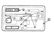
- a contact Chip 1 with a corresponding contact field On the chip card shown in the drawing are a contact Chip 1 with a corresponding contact field, a non-contact one Chip 2, as well as a solar cell 3 and an optical display in the form of a LCD display 4 arranged.
- a battery 5 is used for buffering or temporarily storing the incident ones Light energy that is converted by the solar cell 3.
- a pressure contact switch 6 serves as a switch between different Operating modes or save.
- the chip 1 with contact is a mirror memory 7 or a so-called Assigned balcony chip that reads the mirror image in the Allows chip 7 existing memory information from chip 1 without having to activate the processor chip 1 itself, i.e. reading can made using the energy supplied by the solar cell 3 become.
- the contact chip 1 and the non-contact chip 2 are connected by means of a data exchange line 8 so that it is possible that both chips at least partially have the same information content.
- the contactless chip 2 is a coil 9 for sending and receiving assigned to communication with a reader / writer.
- a capacitor control module 10 enables in the capacitor to store electrical energy and thereby a peak energy requirement cover up.
- the solar cell can also use energy for computing operations or deliver the chips.
- the capacitor control module can, in addition to the aforementioned energy storage to cover the peak demand also excess energy in the contactless area or excess energy from a reader / writer or save unused energy.
- optical display can be static, i.e. the displayed one Storage information remains there for longer periods without further notice Energy supply visible.
Landscapes
- Engineering & Computer Science (AREA)
- General Physics & Mathematics (AREA)
- Physics & Mathematics (AREA)
- Microelectronics & Electronic Packaging (AREA)
- Theoretical Computer Science (AREA)
- Computer Hardware Design (AREA)
- Business, Economics & Management (AREA)
- Computer Security & Cryptography (AREA)
- Life Sciences & Earth Sciences (AREA)
- Sustainable Development (AREA)
- Computer Networks & Wireless Communication (AREA)
- Sustainable Energy (AREA)
- Accounting & Taxation (AREA)
- Strategic Management (AREA)
- General Business, Economics & Management (AREA)
- Credit Cards Or The Like (AREA)
- Photoreceptors In Electrophotography (AREA)
- Dry Shavers And Clippers (AREA)
- Electrochromic Elements, Electrophoresis, Or Variable Reflection Or Absorption Elements (AREA)
Claims (6)
- Carte à puce comprenant une puce de mémoire contenant des informations mémoire et ou une puce à microprocesseur ainsi qu'une possibilité d'affichage (4) avec une alimentation de tension, caractérisée par une mémoire symétrique (7) sur laquelle sont transférées à chaque procédure de travail de la puce mémoire et de la puce à microprocesseur (1, 2) les nouvelles informations internes de mémoire en association avec un appareil externe d'écriture et ou de lecture de sorte que la mémoire symétrique(7) présente des informations de mémoire correspondant aux contenus de mémoire dans la puce à mémoire et/ou dans la puce à microprocesseur (1, 2), la mémoire symétrique (7) étant reliée à la possibilité d'affichage (4) de sorte que les informations qui y sont stockées puissent être affichées au moyen de la possibilité d'affichage (4) sans avoir besoin d'activer la puce à mémoire et/ou la puce à microprocesseur.
- Carte à puce selon la revendication 1, caractérisée par un dispositif de commutation relié à une puce à mémoire et/ou une puce à microprocesseur (1, 2), en particulier un dispositif de commutation de résistance pour la commutation entre les modes de fonctionnement de cartes à puce et/ou des contenus de mémoire pour permettre un affichage commutable par défilement.
- Carte à puce selon la revendication 1 ou 2, caractérisée en ce qu'une bobine d'accord (9) est disposée sur la carte et est de préférence réalisée par pression.
- Carte à puce selon la revendication 1 ou 2, caractérisée en ce que la cellule solaire (3) est associée à un support de mémoire, de préférence sous forme d'une pile (5) et/ou d'un condensateur.
- Carte à puce selon la revendication 1 ou 2, caractérisée en ce qu'elle présente un champ d'identification qui permet la lecture de données relatives à la personne, telles qu'une empreinte digitale pour les comparer à des données d'authentification correspondantes stockées précédemment dans la puce mémoire.
- Carte à puce selon la revendication 1 ou 2, caractérisée en ce que qu'au moins une puce à mémoire ou une puce à microprocesseur (1) sans contact et au moins une puce à mémoire ou une puce à microprocesseur (2) à contact sont prévues et sont reliées entre elles de manière à présenter respectivement au moins partiellement le même contenu d'informations.
Applications Claiming Priority (9)
| Application Number | Priority Date | Filing Date | Title |
|---|---|---|---|
| DE19546189 | 1995-12-11 | ||
| DE19546189 | 1995-12-11 | ||
| DE19610505 | 1996-03-18 | ||
| DE19610505 | 1996-03-18 | ||
| DE19615142 | 1996-04-17 | ||
| DE19615142 | 1996-04-17 | ||
| DE19621597 | 1996-05-30 | ||
| DE19621597 | 1996-05-30 | ||
| PCT/EP1996/005487 WO1997022084A1 (fr) | 1995-12-11 | 1996-12-07 | Carte a puce |
Publications (2)
| Publication Number | Publication Date |
|---|---|
| EP0867014A1 EP0867014A1 (fr) | 1998-09-30 |
| EP0867014B1 true EP0867014B1 (fr) | 2003-03-26 |
Family
ID=27438246
Family Applications (1)
| Application Number | Title | Priority Date | Filing Date |
|---|---|---|---|
| EP96946372A Expired - Lifetime EP0867014B1 (fr) | 1995-12-11 | 1996-12-07 | Carte a puce |
Country Status (7)
| Country | Link |
|---|---|
| US (1) | US6390373B1 (fr) |
| EP (1) | EP0867014B1 (fr) |
| JP (1) | JP2000501862A (fr) |
| AT (1) | ATE235721T1 (fr) |
| AU (1) | AU2845997A (fr) |
| DE (1) | DE59610279D1 (fr) |
| WO (1) | WO1997022084A1 (fr) |
Families Citing this family (23)
| Publication number | Priority date | Publication date | Assignee | Title |
|---|---|---|---|---|
| DE19757863A1 (de) * | 1997-12-24 | 1999-07-08 | Peter Grohse | Sende- und Empfangseinheit zum Bezahlen von Autobahngebühren |
| IL137498A0 (en) * | 1998-01-27 | 2001-07-24 | Viztec Inc | Transmitting advertisements to smart cards |
| DE19816860A1 (de) * | 1998-03-06 | 1999-11-18 | Deutsche Telekom Ag | Chipkarte, insbesondere Guthabenkarte |
| US20120195018A1 (en) * | 2005-11-22 | 2012-08-02 | Lex Kosowsky | Wireless communication device using voltage switchable dielectric material |
| FI111998B (fi) * | 1999-12-08 | 2003-10-15 | Nokia Corp | Käyttöliittymä |
| MXPA02011695A (es) * | 2000-06-28 | 2004-02-12 | Holdings Ltd G | Sistema de transaccion con dispositivo personal portatil de identificacion y de control de transaccion. |
| DE10035094A1 (de) * | 2000-07-17 | 2002-03-28 | Giesecke & Devrient Gmbh | Anzeigevorrichtung für einen tragbaren Datenträger |
| CN1537301A (zh) * | 2001-03-16 | 2004-10-13 | G���ع�����˾ | 在便携式事务处理装置上替换标识数据的系统和方法 |
| JP4863035B2 (ja) * | 2001-06-20 | 2012-01-25 | 大日本印刷株式会社 | 情報表示カード |
| JP2006510085A (ja) * | 2002-12-12 | 2006-03-23 | コーニンクレッカ フィリップス エレクトロニクス エヌ ヴィ | 温度を感知する電子インクを使用した不揮発性ディスプレイを有するスマートカード |
| WO2004090805A1 (fr) * | 2003-04-14 | 2004-10-21 | G. Holdings Ltd. | Dispositif electronique portatif permettant des operations de transfert de donnees en alternat suite a une instruction d'activation invariable |
| US9022294B2 (en) * | 2003-04-14 | 2015-05-05 | G. Holdings Ltd. | Portable electronic device and method for alternate data conveyance operations responsive to an invariable activation command |
| US7937593B2 (en) * | 2004-08-06 | 2011-05-03 | Broadcom Corporation | Storage device content authentication |
| US7252242B2 (en) * | 2005-02-04 | 2007-08-07 | Chun-Hsin Ho | Method for providing additional service based on dual UICC |
| FI118779B (fi) * | 2005-10-07 | 2008-03-14 | Riku Rikkola | Kortti, kortin vastaanottolaite ja järjestelmä sähköenergian välittämistä varten |
| JP4867298B2 (ja) * | 2005-11-09 | 2012-02-01 | 大日本印刷株式会社 | Icカード |
| ES2310075B1 (es) * | 2006-01-12 | 2009-11-05 | Cesar Sanchez Ceballos | Tarjeta electronica con chip incorporado. |
| KR20080036686A (ko) * | 2006-10-24 | 2008-04-29 | 삼성전자주식회사 | 외부 광원을 이용한 정보 표시 기능을 갖는 메모리 카드와정보 표시 방법 |
| ATE530996T1 (de) * | 2009-04-09 | 2011-11-15 | NagraID Security SA | Karte vom typ bankkarte mit einem durch den benutzer aktivierbaren schalter |
| DE102015010458A1 (de) * | 2015-08-11 | 2017-02-16 | Giesecke & Devrient Gmbh | Tragbarer Datenträger, inbesondere Chipkarte |
| EP3349151B1 (fr) * | 2017-01-11 | 2019-11-06 | Mohammad Khaled Asef | Bouton-poussoir double face ayant une fonction tactile |
| US20230297805A1 (en) * | 2022-03-17 | 2023-09-21 | Capital One Services, Llc | Finger-activated chip or contactless card |
| WO2025158664A1 (fr) * | 2024-01-26 | 2025-07-31 | 株式会社Nttドコモ | Carte à puce |
Family Cites Families (7)
| Publication number | Priority date | Publication date | Assignee | Title |
|---|---|---|---|---|
| US4800255A (en) * | 1986-08-22 | 1989-01-24 | Datatrak, Inc. | Electronic access card with visual display |
| JPH04182893A (ja) * | 1990-11-19 | 1992-06-30 | Nec Eng Ltd | 端末装置 |
| DE4121023C2 (de) * | 1991-06-26 | 1994-06-01 | Smartdiskette Gmbh | In eine EDV-Einrichtung einsteckbares Element |
| NL9101608A (nl) * | 1991-09-24 | 1993-04-16 | Nedap Nv | Chipkaart met identificatiemogelijkheid op afstand. |
| DE4203748A1 (de) * | 1992-02-04 | 1993-08-05 | Provera Ges Fuer Projektierung | Verfahren und einrichtung zur mehrfachnutzung und auswertung von wiederaufladbaren chip-karten |
| DE9310271U1 (de) * | 1993-07-09 | 1993-09-02 | Siemens AG, 80333 München | Mobiler Datenspeicher mit Display |
| US6068183A (en) * | 1998-04-17 | 2000-05-30 | Viztec Inc. | Chip card system |
-
1996
- 1996-12-07 JP JP09521723A patent/JP2000501862A/ja active Pending
- 1996-12-07 AT AT96946372T patent/ATE235721T1/de not_active IP Right Cessation
- 1996-12-07 AU AU28459/97A patent/AU2845997A/en not_active Abandoned
- 1996-12-07 EP EP96946372A patent/EP0867014B1/fr not_active Expired - Lifetime
- 1996-12-07 DE DE59610279T patent/DE59610279D1/de not_active Expired - Lifetime
- 1996-12-07 US US09/091,091 patent/US6390373B1/en not_active Expired - Fee Related
- 1996-12-07 WO PCT/EP1996/005487 patent/WO1997022084A1/fr not_active Ceased
Also Published As
| Publication number | Publication date |
|---|---|
| US6390373B1 (en) | 2002-05-21 |
| EP0867014A1 (fr) | 1998-09-30 |
| JP2000501862A (ja) | 2000-02-15 |
| DE59610279D1 (de) | 2003-04-30 |
| ATE235721T1 (de) | 2003-04-15 |
| WO1997022084A1 (fr) | 1997-06-19 |
| AU2845997A (en) | 1997-07-03 |
Similar Documents
| Publication | Publication Date | Title |
|---|---|---|
| EP0867014B1 (fr) | Carte a puce | |
| EP1303835B1 (fr) | Support de donnees portable | |
| EP0920675B1 (fr) | Systeme de traitement d'informations presentant un support en forme de carte muni d'un affichage | |
| EP0774144B1 (fr) | Carte a puce | |
| EP0834155B1 (fr) | Procede de distribution de cartes a puce | |
| EP0784301B1 (fr) | Méthode et système pour le paiement de services et support de données portable à utiliser dans un tel système | |
| DE3906349C2 (fr) | ||
| DE3687186T2 (de) | Transaktionskarte. | |
| DE69807513T2 (de) | Tragbare chipkarte | |
| DE2560080C2 (de) | Datenaustauschanordnung | |
| DE69423368T2 (de) | Reise-registrierungssystem | |
| DE102005008258A1 (de) | Datenträger mit TAN-Generator und Display | |
| DE60224235T2 (de) | Intelligente Dokumente | |
| EP0340222A1 (fr) | Dispositif manuel portatif de traitement automatique de donnees enregistrees sur des supports de donnees. | |
| EP0260221A2 (fr) | Méthode pour la transmission d'information sans contact | |
| DD282308A5 (de) | Schaltungsanordnung mit einer zumindest einen teil der anordnung enthaltenden karte fuer geschaefts-, indentifizierungs- und/oder betaetigungszwecke | |
| DE19629351C2 (de) | Mobiles Chipkarten-Lesemodul | |
| EP0815530B1 (fr) | Procede et dispositif permettant d'adapter une carte a puce a differents terminaux de cartes | |
| EP3264337B1 (fr) | Adaptateur pour un appareil de lecture | |
| DE4138131A1 (de) | Kontaktlose chip-karte mit integriertem mikroprozessor und vorrichtung zum lesen und eingeben von informationen | |
| WO1997008645A2 (fr) | Carte plastique pourvue d'une ou plusieurs puces | |
| DE4203748A1 (de) | Verfahren und einrichtung zur mehrfachnutzung und auswertung von wiederaufladbaren chip-karten | |
| EP1055207A1 (fr) | Procede pour commander un echange d'informations et de donnees entre un telephone mobile et un reseau de transmission de donnees | |
| DE19544144C2 (de) | Verfahren zur Datenübertragung zwischen Datenträgerkarten | |
| DE4027735A1 (de) | Verfahren und vorrichtung zur gesicherten datenfernuebermittlung |
Legal Events
| Date | Code | Title | Description |
|---|---|---|---|
| PUAI | Public reference made under article 153(3) epc to a published international application that has entered the european phase |
Free format text: ORIGINAL CODE: 0009012 |
|
| 17P | Request for examination filed |
Effective date: 19980713 |
|
| AK | Designated contracting states |
Kind code of ref document: A1 Designated state(s): AT BE CH DE DK ES FI FR GB GR IE IT LI LU MC NL PT SE |
|
| 17Q | First examination report despatched |
Effective date: 19990205 |
|
| GRAG | Despatch of communication of intention to grant |
Free format text: ORIGINAL CODE: EPIDOS AGRA |
|
| GRAG | Despatch of communication of intention to grant |
Free format text: ORIGINAL CODE: EPIDOS AGRA |
|
| GRAH | Despatch of communication of intention to grant a patent |
Free format text: ORIGINAL CODE: EPIDOS IGRA |
|
| GRAH | Despatch of communication of intention to grant a patent |
Free format text: ORIGINAL CODE: EPIDOS IGRA |
|
| GRAA | (expected) grant |
Free format text: ORIGINAL CODE: 0009210 |
|
| RBV | Designated contracting states (corrected) |
Designated state(s): AT CH DE ES FR GB IE IT LI NL SE |
|
| AK | Designated contracting states |
Designated state(s): AT CH DE ES FR GB IE IT LI NL SE |
|
| PG25 | Lapsed in a contracting state [announced via postgrant information from national office to epo] |
Ref country code: NL Free format text: LAPSE BECAUSE OF FAILURE TO SUBMIT A TRANSLATION OF THE DESCRIPTION OR TO PAY THE FEE WITHIN THE PRESCRIBED TIME-LIMIT Effective date: 20030326 Ref country code: IT Free format text: LAPSE BECAUSE OF FAILURE TO SUBMIT A TRANSLATION OF THE DESCRIPTION OR TO PAY THE FEE WITHIN THE PRE;WARNING: LAPSES OF ITALIAN PATENTS WITH EFFECTIVE DATE BEFORE 2007 MAY HAVE OCCURRED AT ANY TIME BEFORE 2007. THE CORRECT EFFECTIVE DATE MAY BE DIFFERENT FROM THE ONE RECORDED.SCRIBED TIME-LIMIT Effective date: 20030326 Ref country code: IE Free format text: LAPSE BECAUSE OF NON-PAYMENT OF DUE FEES Effective date: 20030326 Ref country code: GB Free format text: LAPSE BECAUSE OF FAILURE TO SUBMIT A TRANSLATION OF THE DESCRIPTION OR TO PAY THE FEE WITHIN THE PRESCRIBED TIME-LIMIT Effective date: 20030326 Ref country code: FR Free format text: LAPSE BECAUSE OF FAILURE TO SUBMIT A TRANSLATION OF THE DESCRIPTION OR TO PAY THE FEE WITHIN THE PRESCRIBED TIME-LIMIT Effective date: 20030326 |
|
| REG | Reference to a national code |
Ref country code: GB Ref legal event code: FG4D Free format text: NOT ENGLISH |
|
| REG | Reference to a national code |
Ref country code: CH Ref legal event code: EP |
|
| REF | Corresponds to: |
Ref document number: 59610279 Country of ref document: DE Date of ref document: 20030430 Kind code of ref document: P |
|
| REG | Reference to a national code |
Ref country code: IE Ref legal event code: FG4D Free format text: GERMAN |
|
| PG25 | Lapsed in a contracting state [announced via postgrant information from national office to epo] |
Ref country code: SE Free format text: LAPSE BECAUSE OF FAILURE TO SUBMIT A TRANSLATION OF THE DESCRIPTION OR TO PAY THE FEE WITHIN THE PRESCRIBED TIME-LIMIT Effective date: 20030626 |
|
| NLV1 | Nl: lapsed or annulled due to failure to fulfill the requirements of art. 29p and 29m of the patents act | ||
| GBV | Gb: ep patent (uk) treated as always having been void in accordance with gb section 77(7)/1977 [no translation filed] |
Effective date: 20030326 |
|
| PG25 | Lapsed in a contracting state [announced via postgrant information from national office to epo] |
Ref country code: ES Free format text: LAPSE BECAUSE OF FAILURE TO SUBMIT A TRANSLATION OF THE DESCRIPTION OR TO PAY THE FEE WITHIN THE PRESCRIBED TIME-LIMIT Effective date: 20030930 |
|
| REG | Reference to a national code |
Ref country code: IE Ref legal event code: FD4D Ref document number: 0867014E Country of ref document: IE |
|
| PG25 | Lapsed in a contracting state [announced via postgrant information from national office to epo] |
Ref country code: AT Free format text: LAPSE BECAUSE OF NON-PAYMENT OF DUE FEES Effective date: 20031207 |
|
| PG25 | Lapsed in a contracting state [announced via postgrant information from national office to epo] |
Ref country code: LI Free format text: LAPSE BECAUSE OF NON-PAYMENT OF DUE FEES Effective date: 20031231 Ref country code: CH Free format text: LAPSE BECAUSE OF NON-PAYMENT OF DUE FEES Effective date: 20031231 |
|
| PLBE | No opposition filed within time limit |
Free format text: ORIGINAL CODE: 0009261 |
|
| STAA | Information on the status of an ep patent application or granted ep patent |
Free format text: STATUS: NO OPPOSITION FILED WITHIN TIME LIMIT |
|
| EN | Fr: translation not filed | ||
| 26N | No opposition filed |
Effective date: 20031230 |
|
| REG | Reference to a national code |
Ref country code: CH Ref legal event code: PL |
|
| PGFP | Annual fee paid to national office [announced via postgrant information from national office to epo] |
Ref country code: DE Payment date: 20120227 Year of fee payment: 16 |
|
| REG | Reference to a national code |
Ref country code: DE Ref legal event code: R119 Ref document number: 59610279 Country of ref document: DE Effective date: 20130702 |
|
| PG25 | Lapsed in a contracting state [announced via postgrant information from national office to epo] |
Ref country code: DE Free format text: LAPSE BECAUSE OF NON-PAYMENT OF DUE FEES Effective date: 20130702 |