EP0867833A2 - Appareil pour le traitement d'information bidimensionelle - Google Patents
Appareil pour le traitement d'information bidimensionelle Download PDFInfo
- Publication number
- EP0867833A2 EP0867833A2 EP98302222A EP98302222A EP0867833A2 EP 0867833 A2 EP0867833 A2 EP 0867833A2 EP 98302222 A EP98302222 A EP 98302222A EP 98302222 A EP98302222 A EP 98302222A EP 0867833 A2 EP0867833 A2 EP 0867833A2
- Authority
- EP
- European Patent Office
- Prior art keywords
- signal
- pulse width
- circuit
- unit cell
- information
- Prior art date
- Legal status (The legal status is an assumption and is not a legal conclusion. Google has not performed a legal analysis and makes no representation as to the accuracy of the status listed.)
- Granted
Links
Images




Classifications
-
- G—PHYSICS
- G06—COMPUTING OR CALCULATING; COUNTING
- G06T—IMAGE DATA PROCESSING OR GENERATION, IN GENERAL
- G06T1/00—General purpose image data processing
- G06T1/20—Processor architectures; Processor configuration, e.g. pipelining
Definitions
- This invention relates to an electronic field for realizing a multi-media information processing system which is used for storing and transmitting compressed information indicative of two-dimensional images, figures, etc., or for realizing a highly intelligent processing system which is used for extracting and recognizing the features of images, figures, etc.
- the conventional image and figure processing systems employ a structure in which information is input by an image sensor, then converted to a digital signal by an AD converter, and processed by a digital signal processor or a microprocessor.
- an information processing system using a digital circuit is most excellent in accuracy and stability, it requires multiple elements since it uses each transistor as a switching element. Increase of the integration scale and the operation speed of the system inevitably increases the energy consumption and limits the performance. Since the information processing architecture in the case of using a digital circuit is basically sequential processing, which is not suitable to parallel processing of two-dimensional information or calculation of multiple inputs employed in a neural network.
- the analog circuit uses a transistor as a linear element such as an amplifier, and processes an analog signal whose level continuously varies with the passing of time.
- the analog circuit performs calculation on the basis of physical basic laws, and hence can realize the same function as the digital circuit, using 1/10 or 1/100 of the elements used in the digital circuit. Further, the former is excellent in relatively roughly grasping a state and judging it as a result of comparison, and is suitable for parallel operation. However, it is hard for the analog circuit to process information with high accuracy. In now available apparatuses each equipped with both analog and digital circuits, AD or DA conversion limits their performance, and noise (cross talk) leaking from the digital circuit to the analog circuit also limits their performance.
- Image or figure processing sensors which have been regarded as more and more important, are mainly provided in the form of CCD devices which treat input information as an analog charge amount. However, these devices are produced in a special process, and hence not suitable to integration with CMOS logic circuits for signal processing.
- the present invention has been developed in light of this, and is applicable to an information processing apparatus for performing detection of two-dimensional information such as an image, figure, etc., compression of information, and extraction of information features.
- the invention aims to provide an energy-saving, highly-performable information processing apparatus close to human intelligence, capable of processing high-level information indicative of images, figures, etc.
- the invention is applicable to an image sensor using a two-dimensional PN junction photodetector as an input device, a function image sensor wherein the image sensor itself has a function for processing pixels, an apparatus for processing two-dimensional information in a parallel manner to compress the information, an apparatus for extracting and recognizing features of a two-dimensional figure or image, a robot's eye device, a figure recognizing apparatus, or a two-dimensional information processing apparatus as an identification processing apparatus for identifying faces, finger prints, etc.
- the invention can reduce the number of elements incorporated in a CMOS or an LSI, to thereby reduce the chip area, increase the throughput and reduce the consumed energy.
- a two-dimensional information processing apparatus in which two-dimensional information is written optically or electrically into unit cells arranged in rows and columns, a ramp signal is selectively applied to the unit cells, and a pulse width modulation (PWM) signal pulse is generated from each of the selected unit cells, which pulse modulation signal rises when the voltage of the ramp signal starts to increase, and falls when the voltage of the ramp signal is identical to a voltage corresponding to the written information.
- PWM signal pulses from the unit cells are applied to a plurality of lines in a parallel manner in units of one row or one column.
- This structure enables production of various apparatuses such as a two-dimensional information processing apparatus for reading information by scanning, an apparatus for calculating sums in units of one row or one column and outputting the calculation results, an apparatus for performing spatial filter calculation using sum-of-product calculation, an apparatus for detecting the position of an edge and outputting a signal indicative of the position, and an apparatus for calculating the sums of the numbers of edges in units of one row or one column and outputting the calculation results.
- Pulse modulation signals which have a two-value amplitude and carry information on a time basis, include a pulse width modulation (PWM) signal, a pulse phase modulation (PPM) signal and a pulse density modulation (PDM) signal.
- the pulse width modulation (PWM) signal has a pulse width indicative of analog information, and is considered as an intermediate signal between an analog signal and a digital signal.
- An analog digital mixture circuit which has both merits of the analog signal and the digital signal can be constituted using the PWM signal. Since a single PWM signal can represent multi-bit information, only a small amount of energy is consumed to perform data transmission or arithmetic operations.
- the present invention uses the PWM signal which has a data transmission and arithmetic function of high accuracy and low energy, for the following purposes:
- FIG. 1A a plurality of unit cell circuits 1 are arranged in a matrix.
- Each unit cell circuit 1 is connected to a corresponding one of a plurality of address lines 3 which extend from an address ramp signal generation circuit 2 in a column direction.
- Each address line 3 can be formed as part of a bus line which includes another signal line.
- the address ramp signal generation circuit 2 supplies each selected cell with a control signal which includes a ramp signal and a ramp start signal.
- the output of each unit cell circuit 1 is connected to a corresponding one of a plurality of bus lines 4 which extend in a row direction and are connected to a pulse-width/charge detection circuit 5 for reading a pulse width modulation output signal.
- FIG. 1B shows an example of a two-dimensionally displayed output obtained by processing the input optical information using the two-dimensional information processing apparatus of the first embodiment.
- FIG. 2A shows an example of the unit cell circuit 1, while FIG. 2B shows the timing chart of the circuit.
- the unit cell circuit 1 has a photodetector 6 and a signal processing circuit 7 connected thereto.
- the signal processing circuit 7 has a function for generating a PWM signal with a pulse width corresponding to the amount of optical information detected by the photodetector 6, and comprises a storage circuit 8, a comparator 9, an AND circuit 10 and an output circuit 11 in this embodiment.
- the photodetector 6 is formed of a PN junction prepared by the LSI technique, or of a photo transistor. Light is converted to current, integrated for a certain period of time and stored as an electric charge in the storage circuit 8.
- the comparator 9 compares a voltage determined from the stored charge with the linearly varying voltage of a ramp signal supplied through a corresponding address line 3.
- the PWM signal pulse is raised when the voltage of the ramp signal starts to increase, and is fallen when the comparator 9 has detected that the voltage determined from the charge stored in the cell and the ramp signal voltage are identical to each other.
- the AND circuit 10 connected to the comparator 9 and a ramp start signal line 12 controls the rise and fall of the PWM pulse on the basis of the ramp start signal and the output of the comparator 9. On the basis of this control, the output circuit 11 connected to the AND circuit 10 generates a PWM signal of a pulse width corresponding to the output of the photodetector 6.
- the signal processing circuit 7 can have any voluntary structure if it generates a PWM signal of a pulse width corresponding to the output of the photodetector 6.
- the two-dimensional information input to the unit cell from the outside is not limited to optical information but may be electric information.
- a detector for detecting electric information is used in place of the photodetector 6.
- the detected information may be directly converted to a PWM signal without being stored in the storage circuit.
- the address ramp signal generation circuit 2 has a function for simultaneously supplying a ramp signal through a corresponding address line 3 to those unit cells which are included in any desired column.
- ramp signal pulses are sequentially supplied to designated address lines (#1, #4), information items in the unit cell circuits connected to the lines can be read as PWM signal pulses in units of one row. Thus, a voluntary column can be accessed at random.
- ramp signal pulses are sequentially supplied to the address lines.
- scan is performed from left to right in the row direction, thereby outputting, as PWM pulses, cell information items included in each column. Since in this operation, rows can be scanned in a parallel manner, the two-dimensional information can be read at high speed.
- serial scanning of two-dimensional information can also be performed by applying a selection signal in the column direction, too. In this case, after PWM pulses of a certain row are outputted, another row to be accessed next is selected using the selection signal.
- the structure can be modified such that in each of the above-described operations, column-directional scanning is performed instead of the row-directional scanning.
- the dynamic range of the PWM signal is determined on the basis of the maximum-pulse-width/time-resolution. It is, of course, necessary to set an appropriate dynamic range in accordance with information to be dealt with.
- noise such as crosstalk is liable to occur since an analog charge is directly transmitted on a transmission line.
- a charge is converted to a PWM signal in each unit cell. The use of the PWM signal prevents the signal quality through the information transmission route such as a bus line, from easily degrading.
- FIG. 5 shows a specific circuit example in which a CMOS is used in the unit cell circuit 1.
- FIG. 5A illustrate the structure of its basic circuit.
- the photodetector 6 consists of a photo transistor 13
- the storage circuit 8 consists of a combination of a MOS transistor 16 serving as a shutter switch and a capacitor 17
- the comparator 9 consists of a CMOS inverter 14 with a resetting feedback switch 15.
- FIG. 5B illustrates the operation of the basic circuit assumed at the time of reset
- FIG. 5C the operation assumed at the time of input integration
- FIG. 5D charge-PWM conversion the charge-PWM conversion.
- FIG. 6 is an operation-wave/timing chart of the circuit.
- the circuit is reset (FIG. 5B), and the feedback switch 15 of the comparator 9 and the shutter switch 16 of the storage circuit 8 are turned on to thereby accumulate, in the capacitor 17, a charge which compensates for fluctuation of the threshold voltage of the inverter 14.
- the photo transistor 13 detects light corresponding to each pixel of a two-dimensional pattern, and a light current corresponding to the detected light is accumulated in the capacitor 17 through the shutter switch 16 (FIG. 5C).
- an address ramp signal is applied to the other terminal 18 of the capacitor 17 after the shutter switch 16 is turned off by a shutter signal from a shutter 19 (FIG. 5D).
- the PWM signal can be generated by connecting a flip flop (not shown) which is set when the ramp signal starts to be raised, and reset when the output of the comparator 9 is inverted.
- accumulation of charge due to light input and the generation of the PWM signal are performed serially, it can be modified such that the accumulation and the generation are performed parallel to each other in a pipelining manner.
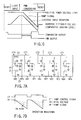
- FIG. 7 shows an example of a five-line address ramp signal generation circuit 2.
- Each line includes a CMOS switch 20, a charge integration capacitor 22, and a MOS transistor 21 for generating a constant current I used at the time of discharge of the MOS transistor 21.
- a ramp control signal CT is at high level, the constant current I flows and the charge of the capacitor 22 is discharged to a ground terminal 23, and therefore the voltage of the capacitor 22 linearly reduces.
- the ramp control signal CT is at low level, the capacitor 22 is rapidly charged, and the ramp signal is set at the voltage Vdd of a positive power 24.
- the wave inclination of the ramp signal (RP0 - RP4) can be set at any voluntary value by controlling the channel width and the gate bias voltage (VB0 - VB4) of the MOS transistor 21.
- the ramp signal (RP0 - RP4) applied to each column is generated by a circuit dedicated thereto and having the same structure as another circuit dedicated to another column. Since the variation range of elements on the integrated circuit chip is relatively small, the ramp signal RP has a high relative accuracy.
- the second embodiment differs from the first embodiment wherein row-directional cell information items are added together in a parallel manner, in that the former employs a current supply driving circuit 25 in place of the output circuit 11 for outputting the PWM signal of the unit cell circuit 1.
- FIG. 8C shows no specific circuit structure of the current supply driving circuit 2. It can have any desired circuit structure.
- FIG. 8C shows only the output circuit of the unit cell circuit 1 and no other elements.
- FIG. 8A is a view, showing an example of a circuit for projecting figure information in both the row and column directions, while FIG. 8B is a timing chart, useful in explaining the operation of the circuit. Since the output impedance of the current supply driving circuit 25 is high, pulse currents of the cells are added together in the bus line 4.
- the address ramp signal generation circuit 2 has a function for simultaneously applying the ramp signal and the PWM signal to each address line 3.
- the sum of all row-directional cell information items can be obtained in the form of a charge by integrating the output current of the bus line 4.
- row-directional cell information items can be added together in an analog manner.
- the addition result is output as digital data from a charge detection circuit/charge-digital conversion circuit 26.
- the charge detection circuit/charge-digital conversion circuit 26 can have a voluntary structure. It suffices if the circuit can detect a charge on each bus line and convert it to a digital amount.
- the circuit can be modified such that column-directional cell information items are added together.
- the address ramp signal generation circuit 2 can be connected to each row, and the charge detection circuit/charge-digital conversion circuit 26 can be connected to each column.
- the addition result is output as digital data from the charge detection circuit/charge-digital conversion circuit 26.
- Appropriate addition is, of course, performed alternately in the row and column directions under the control of a control circuit (not shown).
- Information obtained by this processing indicates a profile of figure information projected in the X- and Y-axis directions (in the horizontal and vertical directions in FIG. 8A, respectively), and is used as feature information on a figure.
- FIG. 9 is a timing chart, useful in explaining the operation performed in the case of outputting a value which is obtained by multiplying the amount of information stored in each unit cell 1 (i.e. the voltage of the capacitor of the cell) by a coefficient, and then adding together the multiplication results.
- ramp signals with waves of different inclinations are applied to different columns to calculate the sum of the cell outputs multiplied by the coefficient, i.e. the sum-of-product concerning the cell outputs.
- the inclination of the ramp signal is controlled by a bias voltage VB applied to the MOS transistor 21 which is incorporated in the address ramp signal generation circuit 2 for generating a constant current.
- a voltage corresponding to the information amount of each cell is compared with that of the ramp signal. This means that the greater the inclination of the ramp signal, the lower the coefficient to be applied to information accumulated in each unit cell (and vice versa).
- PWM signals from the unit cells are integrated as a current supply output through the bus line 4.
- the integrated charge is the result of sum-of-product calculation.
- one-dimensional spatial filter calculation can be performed in a parallel manner. It is a matter of course that the third embodiment can be modified to perform column-directional sum-of-product calculation instead of the row-directional sum-of-product calculation.
- the discrete cosine conversion can be realized by providing a positive polarity bus 27 and a negative polarity bus 28, integrating positive outputs in the positive polarity bus and negative outputs in the negative polarity bus, respectively, and calculating the difference therebetween.
- the fourth embodiment differs from the third embodiment in that an edge detection circuit 29 is used in place of the charge detection circuit/charge-digital conversion circuit 26.
- This structure enables detection of a two-dimensional pattern edge.
- two kinds of bus lines i.e. an even number bus line 30 and an odd number bus line 31, are employed and connected to each even number cell and each odd number cell, respectively.
- Ramp signals are applied to a voluntary cell and a cell adjacent thereto, and PWM signals output from the cells are applied to an EXOR circuit 32 through the even number/odd number bas lines, thereby to calculate the difference in pulse width therebetween. When the pulse width difference exceeds a predetermined threshold value, it is determined that an edge exists.
- the sign of the edge (left > right, right > left) can be determined by calculating the logical product of the output of the EXOR circuit 32 and the output of the even number bus line 30, and the logical product of the output of the ECOR circuit 32 and the output of the odd number bus line 31.
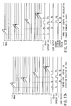
- the position of the edge can be read using the ramp signal as its address, as is shown in FIG. 13(a). This edge information is extremely important to process an image of a figure.
- the sum of the numbers of row-directional edges can be obtained by sequentially and row-directionally scanning two ramp signals applied to even and odd cells, applying the PWM signals output from the cells to the EXOR circuit 32, outputting the difference between the output signals of the even and odd cells, binarizing the output difference, using a binarizing circuit 33, when it exceeds a threshold value, and counting, using a counter circuit 34, the number of signal pulses output from the binarizing circuit, as is shown in FIG. 13B. If scanning is performed in the column direction, the sum of the numbers of column-directional edges can be obtained. This edge information is also useful as feature information on a figure.
- Each of the binarizing circuit 33 and the counter circuit 34 can be formed of any voluntary circuit. The comparison of the output difference with the threshold value is performed using a voluntary comparison circuit (not shown).
- This comparison processing is performed simultaneously in rows. Naturally, the processing can be modified to be performed simultaneously in columns. Since the feature of a figure is expressed by a one-dimensionally projected profile, the shape of each edge, or the number of edges, the figure can be recognized by comparing the feature with a reference template and selecting a most similar one.
- the invention has the following advantages: Since information in each cell is processed on the two-dimensional surface of a sensor, high-level processing can be performed which is impossible in the conventional case where a CCD image sensor as a serial scanner is used. Since the invention employs an analog/digital mixture circuit using PWM signals, the number of required elements can be reduced to 1/10 or 1/100. A small number of elements enables a device of a small chip area. Further, since multiple inputs can be processed in an analog manner and in a parallel manner, the processing capacity can be increased by 10 times. Since there are a small number of circuit nodes in the invention and the voltage transition frequency therein is low, the consumed energy can be reduced to 1/10 or 1/100. Since the invention is suitable for fine CMOS device techniques of the order of 0.1 micron or less, it is considered that the invention will serve as a basic technique for future intelligent information processing systems, and impact on the industry.
Landscapes
- Physics & Mathematics (AREA)
- General Physics & Mathematics (AREA)
- Engineering & Computer Science (AREA)
- Theoretical Computer Science (AREA)
- Transforming Light Signals Into Electric Signals (AREA)
- Image Analysis (AREA)
- Image Processing (AREA)
- Storing Facsimile Image Data (AREA)
- Static Random-Access Memory (AREA)
Applications Claiming Priority (3)
| Application Number | Priority Date | Filing Date | Title |
|---|---|---|---|
| JP78025/97 | 1997-03-28 | ||
| JP9078025A JP2879670B2 (ja) | 1997-03-28 | 1997-03-28 | 2次元情報処理装置 |
| JP7802597 | 1997-03-28 |
Publications (3)
| Publication Number | Publication Date |
|---|---|
| EP0867833A2 true EP0867833A2 (fr) | 1998-09-30 |
| EP0867833A3 EP0867833A3 (fr) | 2000-06-07 |
| EP0867833B1 EP0867833B1 (fr) | 2002-06-26 |
Family
ID=13650281
Family Applications (1)
| Application Number | Title | Priority Date | Filing Date |
|---|---|---|---|
| EP98302222A Expired - Lifetime EP0867833B1 (fr) | 1997-03-28 | 1998-03-24 | Appareil pour le traitement d'information bidimensionelle |
Country Status (4)
| Country | Link |
|---|---|
| US (1) | US6088490A (fr) |
| EP (1) | EP0867833B1 (fr) |
| JP (1) | JP2879670B2 (fr) |
| DE (1) | DE69806197T2 (fr) |
Cited By (2)
| Publication number | Priority date | Publication date | Assignee | Title |
|---|---|---|---|---|
| WO2007101360A1 (fr) * | 2006-03-06 | 2007-09-13 | Waeny Martin | Capteur d'image miniaturisé |
| EP1509754A4 (fr) * | 2002-06-06 | 2008-01-02 | Semi Conductor Devices Scd Par | Processeur a plan focal pour detection infrarouge |
Families Citing this family (18)
| Publication number | Priority date | Publication date | Assignee | Title |
|---|---|---|---|---|
| US6191534B1 (en) * | 1999-07-21 | 2001-02-20 | Infineon Technologies North America Corp. | Low current drive of light emitting devices |
| US7054850B2 (en) * | 2000-06-16 | 2006-05-30 | Canon Kabushiki Kaisha | Apparatus and method for detecting or recognizing pattern by employing a plurality of feature detecting elements |
| JP2002358523A (ja) * | 2001-05-31 | 2002-12-13 | Canon Inc | パターン認識処理装置及びその方法、画像入力装置 |
| US7085749B2 (en) * | 2001-05-31 | 2006-08-01 | Canon Kabushiki Kaisha | Pulse signal circuit, parallel processing circuit, pattern recognition system, and image input system |
| US7007002B2 (en) | 2001-05-31 | 2006-02-28 | Canon Kabushiki Kaisha | Signal processing circuit involving local synchronous behavior |
| DE602004022229D1 (de) * | 2003-09-12 | 2009-09-10 | Canon Kk | Bildlesegerät und Bilderzeugungssystem mittels Röntgenstrahlen |
| JP4053007B2 (ja) | 2004-01-09 | 2008-02-27 | シャープ株式会社 | 固体撮像素子およびその信号読み出し方法 |
| JP4780921B2 (ja) | 2004-03-17 | 2011-09-28 | キヤノン株式会社 | 並列パルス信号処理装置、及びその制御方法 |
| GB2421374B (en) * | 2004-12-15 | 2007-01-10 | Micron Technology Inc | Ramp generators for imager analog-to-digital converters |
| US7923674B2 (en) | 2005-06-29 | 2011-04-12 | National University Corporation NARA Institute of Science and Technology | Solid-state image sensor having a voltage applier and signal readout method thereof |
| JP2007127628A (ja) * | 2005-10-07 | 2007-05-24 | Topcon Corp | 位置検出装置及びこれを使用した測量機の傾斜センサ装置 |
| US7652706B2 (en) * | 2006-02-15 | 2010-01-26 | Eastman Kodak Company | Pixel analog-to-digital converter using a ramped transfer gate clock |
| US9235499B2 (en) * | 2011-12-16 | 2016-01-12 | General Electric Company | System and method for identifying a character-of-interest |
| US9658347B2 (en) * | 2015-06-15 | 2017-05-23 | General Electric Company | Digital X-ray detector having multi-tap pixels |
| CN105681787B (zh) * | 2016-01-22 | 2019-01-18 | 北京大学 | 对时空信号进行编码的方法和装置 |
| US12452416B2 (en) | 2016-01-22 | 2025-10-21 | Spike Vision (Beijing) Technology Co., Ltd. | Generating image based on pulse sequences obtained from encoded information |
| US11228758B2 (en) | 2016-01-22 | 2022-01-18 | Peking University | Imaging method and device |
| WO2025079417A1 (fr) * | 2023-10-13 | 2025-04-17 | ソニーセミコンダクタソリューションズ株式会社 | Dispositif de détection de lumière et procédé de détection de lumière |
Family Cites Families (4)
| Publication number | Priority date | Publication date | Assignee | Title |
|---|---|---|---|---|
| DE3506749A1 (de) * | 1984-02-27 | 1985-09-26 | Nippon Telegraph & Telephone Public Corp., Tokio/Tokyo | Matrixprozessor und steuerverfahren hierfuer |
| US4835617A (en) * | 1986-09-22 | 1989-05-30 | Hitachi, Ltd. | Image pickup device for television cameras having a shutter function for a photodiode matrix operated using MOS switches |
| US5166539A (en) * | 1990-07-09 | 1992-11-24 | Nippon Telegraph And Telephone Corporation | Neural network circuit |
| US5321639A (en) * | 1992-03-02 | 1994-06-14 | Regents Of The University Of California | Dual-scale topology optoelectronic matrix algebraic processing system |
-
1997
- 1997-03-28 JP JP9078025A patent/JP2879670B2/ja not_active Expired - Fee Related
-
1998
- 1998-03-24 EP EP98302222A patent/EP0867833B1/fr not_active Expired - Lifetime
- 1998-03-24 DE DE69806197T patent/DE69806197T2/de not_active Expired - Fee Related
- 1998-03-25 US US09/047,378 patent/US6088490A/en not_active Expired - Lifetime
Cited By (2)
| Publication number | Priority date | Publication date | Assignee | Title |
|---|---|---|---|---|
| EP1509754A4 (fr) * | 2002-06-06 | 2008-01-02 | Semi Conductor Devices Scd Par | Processeur a plan focal pour detection infrarouge |
| WO2007101360A1 (fr) * | 2006-03-06 | 2007-09-13 | Waeny Martin | Capteur d'image miniaturisé |
Also Published As
| Publication number | Publication date |
|---|---|
| EP0867833A3 (fr) | 2000-06-07 |
| JP2879670B2 (ja) | 1999-04-05 |
| DE69806197T2 (de) | 2003-01-30 |
| EP0867833B1 (fr) | 2002-06-26 |
| JPH10269345A (ja) | 1998-10-09 |
| US6088490A (en) | 2000-07-11 |
| DE69806197D1 (de) | 2002-08-01 |
Similar Documents
| Publication | Publication Date | Title |
|---|---|---|
| US6088490A (en) | Apparatus for processing two-dimensional information | |
| US12010447B2 (en) | Dynamic vision sensor architecture | |
| EP1788802A1 (fr) | Dispositif de sélection d'image, procédé de traitement du résultat de la sélection d'image et circuit intégré | |
| EP1416424B1 (fr) | Réseau de photodétecteurs avec une comparaison de signal au niveau du pixel | |
| US6476860B1 (en) | Center of mass detection via an active pixel sensor | |
| CN113610022A (zh) | 指纹识别电路、显示面板及其控制方法 | |
| KR100191450B1 (ko) | 반도체 장치, 이 장치를 사용하는 반도체 회로, 상관연산장치,신호변환기,및이변환기를사용하는신호처리시스템 | |
| US6631217B1 (en) | Image processor | |
| Brajovic et al. | Temporal photoreception for adaptive dynamic range image sensing and encoding | |
| CN116520350B (zh) | 一种感算一体的激光雷达探测芯片 | |
| CN109584278B (zh) | 一种目标识别装置及方法 | |
| Kawaguchi et al. | Motion detecting artificial retina model by two-dimensional multi-layered analog electronic circuits | |
| EP0772143B1 (fr) | Circuit de traitement de signaux parallèles | |
| Zavidovique et al. | Generic functions for on-chip vision | |
| JP2683189B2 (ja) | 画像処理装置 | |
| JP3453896B2 (ja) | 2値化回路、これを有する固体撮像装置及びこれを用いたバーコード読取り装置 | |
| JPH0652321A (ja) | 情報処理装置 | |
| Niki et al. | Moving-object-localization hardware algorithm employing OR-amplification of pixel activities | |
| Lin et al. | A high-speed target tracking CMOS image sensor | |
| Takeda et al. | A smart imager for the vision processing front-end | |
| Tanner et al. | Single-chip imager and feature extractor | |
| JP2004362462A (ja) | 画像検出処理装置 | |
| Katayama et al. | A High-Resolution Hadamard Transform Circuit Using Pulse Width Modulation Technique | |
| Cho et al. | FPGA based Dynamic Thresholding Circuit | |
| JP2002073588A (ja) | アダマール変換回路 |
Legal Events
| Date | Code | Title | Description |
|---|---|---|---|
| PUAI | Public reference made under article 153(3) epc to a published international application that has entered the european phase |
Free format text: ORIGINAL CODE: 0009012 |
|
| 17P | Request for examination filed |
Effective date: 19980415 |
|
| AK | Designated contracting states |
Kind code of ref document: A2 Designated state(s): DE FR GB |
|
| AX | Request for extension of the european patent |
Free format text: AL;LT;LV;MK;RO;SI |
|
| PUAL | Search report despatched |
Free format text: ORIGINAL CODE: 0009013 |
|
| AK | Designated contracting states |
Kind code of ref document: A3 Designated state(s): AT BE CH DE DK ES FI FR GB GR IE IT LI LU MC NL PT SE |
|
| AX | Request for extension of the european patent |
Free format text: AL;LT;LV;MK;RO;SI |
|
| AKX | Designation fees paid |
Free format text: DE FR GB |
|
| GRAG | Despatch of communication of intention to grant |
Free format text: ORIGINAL CODE: EPIDOS AGRA |
|
| 17Q | First examination report despatched |
Effective date: 20010910 |
|
| GRAG | Despatch of communication of intention to grant |
Free format text: ORIGINAL CODE: EPIDOS AGRA |
|
| GRAH | Despatch of communication of intention to grant a patent |
Free format text: ORIGINAL CODE: EPIDOS IGRA |
|
| GRAH | Despatch of communication of intention to grant a patent |
Free format text: ORIGINAL CODE: EPIDOS IGRA |
|
| GRAA | (expected) grant |
Free format text: ORIGINAL CODE: 0009210 |
|
| AK | Designated contracting states |
Kind code of ref document: B1 Designated state(s): DE FR GB |
|
| REG | Reference to a national code |
Ref country code: GB Ref legal event code: FG4D |
|
| REF | Corresponds to: |
Ref document number: 69806197 Country of ref document: DE Date of ref document: 20020801 |
|
| ET | Fr: translation filed | ||
| PLBE | No opposition filed within time limit |
Free format text: ORIGINAL CODE: 0009261 |
|
| STAA | Information on the status of an ep patent application or granted ep patent |
Free format text: STATUS: NO OPPOSITION FILED WITHIN TIME LIMIT |
|
| 26N | No opposition filed |
Effective date: 20030327 |
|
| PGFP | Annual fee paid to national office [announced via postgrant information from national office to epo] |
Ref country code: FR Payment date: 20040218 Year of fee payment: 7 |
|
| PGFP | Annual fee paid to national office [announced via postgrant information from national office to epo] |
Ref country code: GB Payment date: 20040324 Year of fee payment: 7 |
|
| PGFP | Annual fee paid to national office [announced via postgrant information from national office to epo] |
Ref country code: DE Payment date: 20040517 Year of fee payment: 7 |
|
| PG25 | Lapsed in a contracting state [announced via postgrant information from national office to epo] |
Ref country code: GB Free format text: LAPSE BECAUSE OF NON-PAYMENT OF DUE FEES Effective date: 20050324 |
|
| PG25 | Lapsed in a contracting state [announced via postgrant information from national office to epo] |
Ref country code: DE Free format text: LAPSE BECAUSE OF NON-PAYMENT OF DUE FEES Effective date: 20051001 |
|
| GBPC | Gb: european patent ceased through non-payment of renewal fee |
Effective date: 20050324 |
|
| PG25 | Lapsed in a contracting state [announced via postgrant information from national office to epo] |
Ref country code: FR Free format text: LAPSE BECAUSE OF NON-PAYMENT OF DUE FEES Effective date: 20051130 |
|
| REG | Reference to a national code |
Ref country code: FR Ref legal event code: ST Effective date: 20051130 |