EP0867921A2 - Substrat und Verfahren dessen Herstellung - Google Patents
Substrat und Verfahren dessen Herstellung Download PDFInfo
- Publication number
- EP0867921A2 EP0867921A2 EP98302216A EP98302216A EP0867921A2 EP 0867921 A2 EP0867921 A2 EP 0867921A2 EP 98302216 A EP98302216 A EP 98302216A EP 98302216 A EP98302216 A EP 98302216A EP 0867921 A2 EP0867921 A2 EP 0867921A2
- Authority
- EP
- European Patent Office
- Prior art keywords
- layer
- porous
- substrate
- substrate member
- porous layer
- Prior art date
- Legal status (The legal status is an assumption and is not a legal conclusion. Google has not performed a legal analysis and makes no representation as to the accuracy of the status listed.)
- Withdrawn
Links
Images


Classifications
-
- H—ELECTRICITY
- H10—SEMICONDUCTOR DEVICES; ELECTRIC SOLID-STATE DEVICES NOT OTHERWISE PROVIDED FOR
- H10P—GENERIC PROCESSES OR APPARATUS FOR THE MANUFACTURE OR TREATMENT OF DEVICES COVERED BY CLASS H10
- H10P95/00—Generic processes or apparatus for manufacture or treatments not covered by the other groups of this subclass
-
- H—ELECTRICITY
- H10—SEMICONDUCTOR DEVICES; ELECTRIC SOLID-STATE DEVICES NOT OTHERWISE PROVIDED FOR
- H10P—GENERIC PROCESSES OR APPARATUS FOR THE MANUFACTURE OR TREATMENT OF DEVICES COVERED BY CLASS H10
- H10P90/00—Preparation of wafers not covered by a single main group of this subclass, e.g. wafer reinforcement
- H10P90/19—Preparing inhomogeneous wafers
- H10P90/1904—Preparing vertically inhomogeneous wafers
- H10P90/1906—Preparing SOI wafers
- H10P90/1914—Preparing SOI wafers using bonding
Definitions
- the present invention relates to a method for producing a semiconductor substrate, and more particularly a method for producing a semiconductor substrate adapted for the formation of an electronic device or an integrated circuit in a single-crystal semiconductor layer on a dielectric separation layer or an insulator, or in a single-crystal compound semiconductor on an Si substrate.
- SOI semiconductor-on-insulator
- the fully depleted MOSFET is expected to achieve a higher speed and a lower power consumption by improvement of a driving power.
- the threshold voltage (V+h) of the MOSFET is generally determined by the impurity concentration of the channel portion, and in case of the fully depleted MOSFET utilizing the SOI structure, the thickness of the depletion layer is also affected by the film thickness of SOI. Consequently, in order to produce the large-area integrated circuits with a high production yield, there has strongly been desired the uniformity of the SOI film thickness.
- the devices formed on the compound semiconductor have excellent features, such as a high speed or light emission, which are not achievable with the silicon substrate.
- Presently such devices are mostly formed by epitaxial growth on a compound semiconductor substrate such as GaAs or the like.
- a compound semiconductor substrate such as GaAs or the like.
- such compound semiconductor substrate has drawbacks of expensiveness, a low mechanical strength, difficulty of preparation of a large area wafer and the like.
- the FIPOS method consists of forming islands of N-type Si layer on the surface of a P-type single-crystal Si substrate by proton implantation (Imai et al., J. Crystal Growth, Vol. 63, 547 (1983)), or by epitaxial growth and patterning, then making only the P-type Si substrate porous by anodizing in HF solution so as to surround the Si islands from the surface side, and achieving dielectric isolation of the N-type Si islands by accelerated oxidation. Since in this method the isolated Si island is determined prior to the device manufacturing step, the freedom of device designing may be limited.
- An oxygen ion implantation method is called SIMOX method, which was originally reported by K. Izumi.
- SIMOX method An oxygen ion implantation method is called SIMOX method, which was originally reported by K. Izumi.
- oxygen ions are implanted with a concentration of 10 17 to 10 18 /cm 2 into an Si wafer, it is annealed at a high temperature of about 1320°C in an argon-oxygen atmosphere, whereby the implanted oxygen ions combine with Si atoms around a depth corresponding to the projected stroke (Rp) of the ion implantation to form a silicon oxide layer.
- Rp projected stroke
- an Si layer present on the oxidized silicon layer and made amorphous by oxygen ion implantation recrystallizes to form a single-crystal silicon layer.
- the number of defects in the surface Si layer was as high as 10 5 /cm 2 , but has been reduced to about 10 2 /cm 2 by maintaining the implanted amount of oxygen ions at about 4 x 10 17 /cm 2 .
- the thicknesses of the surface Si layer and the burried Si oxide (BOX: burried oxide) layer have been limited to specified values. Therefore, for obtaining the surface Si layer of a desired film thickness, it has been necessary to effect sacrificed oxidation or epitaxial growth. In such case, there is a problem that the uniformity of the film thickness is inevitably deteriorated since the deterioration of the uniformity of the film thickness due to such process is added to the original film thickness distribution.
- the BOX layer contains a region, called "pipe", of defective formation of Si oxide.
- One of the causes of such defective formation is foreign matters such as dust at the implantation.
- In the portion of such pipe there is generated a leak between an active layer and a supporting substrate to deteriorate the device characteristics.
- the ion implantation of the SIMOX method with a larger amount of implantation in comparison with that in the ordinary semiconductor process requires a long implantation time even by using an developed apparatus exclusive for this purpose. Since the ion implantation is conducted by rester scanning with an ion beam of a predetermined current or by expanding an ion beam, it is anticipated to require a longer time with increase in area of the wafer. Also the high-temperature heat treatment of a wafer having a large area is anticipated to become more difficult, because of the generation of problems such as slip due to the temperature distribution within the wafer. As the SIMOX method requires a heat treatment at 1300°C or higher which is not usually employed in the Si semiconductor process, there is concerned an increase in the problems to be solved such as apparatus development, metal contamination and slip.
- the surface after the plasma etching is coarse, there is required a touch polishing operation is required after the plasma etching, but the difficulty in the control of the final film thickness and the deterioration of the film thickness distribution by the polishing operation are pointed out since the polished amount is controlled by the polishing time.
- the polishing material such as colloidal silica comes into direct contact with the surface of an active layer in the polishing operation, there are concerned the formation of a crushed layer and the generation of a working strain due to the polishing operation.
- the plasma etching time increases proportionally with increase in the wafer area to possibly lead a significant decrease in a throughput.
- the above method 3 consists of providing in advance a substrate to be formed into a thin film structure which can be selectively etched.
- a substrate to be formed into a thin film structure which can be selectively etched.
- a thin P + -type Si layer containing boron atoms at a concentration of 10 19 /cm 3 or more and a thin P-type Si layer are stacked for example by epitaxial growth to obtain a first substrate.
- This substrate is adhered to a second substrate with interposition of an insulating layer such as an oxide film, and the first substrate is made thin by grinding and polishing from the rear surface.
- the selective etching method is considered to be effective for obtaining a uniform thin film, but has with the following problems.
- the selectivity of the selective etching is greatly depended on a difference in a concentration of the impurity such as boron and the steepness of profile of the impurity in the direction of depth. Therefore, if there is conducted a high-temperature bonding annealing for increasing a bonding strength or a high-temperature epitaxial growth for improving a crystallinity, the distribution of the impurity concentration is spread in the direction of depth, thereby deteriorating the etching selectivity. That is the improvement in the etching selectivity has not easily been compatible with the improvement in the crystallinity and in the bonding strength.
- the first substrate is made thin, for example, by grinding from the rear surface to expose the porous Si layer over the entire area of the substrate (Fig. 5B).
- the exposed porous Si is removed by etching with a selective etching solution such as KOH or HF + H 2 O 2 (Fig. 5C).
- a selective etching solution such as KOH or HF + H 2 O 2 (Fig. 5C).
- the selective ratio of the etching of porous Si to bulk Si can be made as high as 100,000 times so that an SOI substrate can be formed by leaving, on the second substrate, the non-porous single-crystal Si layer grown in advance on the porous layer, without any substantial change in the film thickness. Therefore, the film thickness uniformity of SOI can be substantially determined by the epitaxially growing operation.
- the epitaxial growth can be conducted in a CVD apparatus employed in the ordinary semiconductor process, there has been achieved a uniformity, for example, of 100 ⁇ 2% according the report of Sato et al. (SSDM 95). Also it has been reported that the crystallinity of the epitaxial Si layer is a satisfactory value of 3.5 x 10 2 /cm 2 .
- Porous Si was found by Uhlir et al. in 1956 in the course of investigation of electropolishing of a semiconductor (A. Uhlir, Bell Syst. Tech. J., Vol. 35, 333 (1956)).
- the porous Si can be formed by anodization of an Si substrate in HF solution, and has a sponge-like shape having minute pores which is formed from a bulk Si by electrolytic etching.
- the pores have a diameter of about several nanometers and formed with a density, for example, of 10 11 /cm 2 , though these are variable depending on the conditions of anodization and the specific resistivity of Si.
- the selectivity of etching depends on a difference in an impurity concentration and a profile thereof in the direction of depth, so that the temperature of heat treatment (in bonding, epitaxial growth, oxidation, etc.) which spreads the distribution of the concentration is limited to about 800°C or lower.
- the heat treatment since the etching rate is determined by a difference between the porous structure and the bulk structure, the heat treatment involves little limitation in the heat treatment temperature and has been reported achievable at about 1180°C.
- the heat treatment after bonding is known to increase the bonding strength of the bonded wafers and to decrease the number and the size of the voids generated in the bonding interface. Also in the etching based on such structural difference, particles eventually deposited on the porous Si do not influence the uniformity of film thickness.
- a thin Si film deposited thereon usually becomes amorphous or polycrystalline at best, reflecting the crystalline irregularity of the substrate, so that a high-performance device cannot be prepared on such substrate. This is based on a fact that the substrate is amorphous and therefore a satisfactory single-crystal layer cannot be obtained by merely depositing an Si layer thereon.
- the semiconductor substrate employing the bonding method always necessitates two wafers, one of which is mostly removed by polishing or etching, thus leading to an increased cost and eventually resulting in the significant waste of the limited resources of the earth.
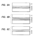
- a single-crystal Si layer 43 is formed thereon, and this single-crystal Si layer 43 is adhered via an insulating layer 45 to the main face of a second Si substrate 44 which is separate from the first substrate 41 (Fig. 6A).
- the bonded wafers are divided by the porous layer (Fig. 6B), and the porous Si layer remaining on the surface of the second Si substrate is selectively removed by etching to obtain a SOI substrate (Fig. 6C).
- the division of the bonded wafers is achieved by destruction of the porous Si layer by:
- porous Si is dependent on the level of porosity, it is considered that the strength is sufficiently lower than that of bulk Si. For example, if the porosity is 50%, the mechanical strength of a porous layer is considered to be about half of that of bulk Si.
- a compressing force, a tensile force or a shearing force is applied to the bonded wafers, the porous Si layer is broken at first.
- the porous layer can be broken with a weaker force by increase in the level of porosity.
- the porosity is defined as percentage of pore volume with respect to the apparent volume of a porous layer, that is, the sum of the volume of a material constituting the porous layer and the pore volume.
- Japanese Patent Application Laid-Open No. 8-213645 describes a method of separation by the porous layer, but does not describe the layer structure of the porous layer.
- Tanakaya et al. of Sony reported, in Preprints for 1996 Fall Congress of Applied Physics society, p.673, the preparation of porous Si by a change in the current in the course of processing.
- the Japanese Patent Application Laid-Open No. 8-213645 describes that the separation takes place at any position of the separation layer, that is, that the separating position cannot be defined.
- the thickness of the remaining porous Si layer fluctuates over the wafer, and, when the porous Si is removed by etching, an active layer (device forming layer) is more or less etched also to result in a fluctuating thickness in the plane of the wafer as long as the etching rate for the active layer consisting of a non-porous single crystal is not zero. Also even if the remaining porous Si is left unremoved, the surface step coverage resulting from the separating position is left on the wafer.
- the etching step of the porous layer has been considered to be essential.
- the etching step requires conveyance of the substrate into and from the etching apparatus, management of the etching apparatus and etchant, rinsing of the substrate after etching, etc. Therefore the preparation time of the SOI substrate can be significantly reduced if the etching step can be omitted.
- An object of the present invention is to provide a method of producing a substrate, which is capable of omitting a selective etching step of the porous layer.
- Another object of the present invention is to provide a method for inexpensively preparing a semiconductor substrate of satisfactory quality, represented by the SOI substrate.
- the present invention provides a method for producing a substrate, comprising:
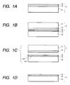
- Figs. 1A to 1D show a basic example of the method of producing a substrate according to the present invention.
- a first substrate member 2 having a first layer 12 and a second layer 13 provided on and adjacent to the first layer.
- Numeral 14 indicates an insulating film.
- the first substrate member 2 and the second substrate member 15 are separated, whereby the second layer 13 is transferred onto an insulating surface 14f of the second substrate member 15.
- the separation takes place at the interface between the first layer 12 and the second layer 13, the first layer does not remain on the exposed surface (separation surface) 13f of the second layer 13 transferred onto the second substrate member 15.
- a substrate 3 having a smooth surface can be obtained without selective etching or selective polishing of the exposed surface 13f of the second layer 13. If necessary, the surface 13f of the second layer 13 of the substrate 3 can be subjected to a smoothing treatment such as heat treatment in a non-oxidative atmosphere.
- the first substrate member employed in the present invention comprises at least the first layer and the second layer which are formed of mutually different materials or have mutually different mechanical strengths.
- a non-porous layer is used as the second layer.
- the material constituting the second layer include Si and compound semiconductors such as GaAs, InP, etc., a metal and carbon, but such examples are not restrictive.
- such layer need not necessarily be formed over the entire surface but may be partially etched by a patterning treatment.
- an insulating layer such as an oxide film may be formed.
- the second substrate member may be an Si member, an Si member having an Si oxide film formed on a surface thereof, a light-transmissive member such as quartz, fused quartz, sapphire or silica glass, or a metal member, but the material constituting the second substrate member is not restrictive.
- the first substrate member and the second substrate member are preferably plate-shaped or disk-shaped.
- insulating layer such as an oxide film
- Figs. 1A to 1D show an example in which the insulating layer 14 is provided on the surface of the second substrate member 15.
- a mechanically weaker separation layer may be formed by using a porous layer at such interface or by ion implantation at such interface. Otherwise the mechanically weaker separation layer may be formed by introducing defects into such interface.
- the separation can be achieved, for example, by the application of an external force such as a pressure, a tensile force, a shearing force or a force by a wedge, application of ultrasonic wave or heat, application of an internal pressure to porous Si by oxidizing porous Si to expand it from the periphery thereof, application of a thermal stress by pulsed heating, or by softening, but these are not restrictive.
- an external force such as a pressure, a tensile force, a shearing force or a force by a wedge
- ultrasonic wave or heat application of an internal pressure to porous Si by oxidizing porous Si to expand it from the periphery thereof
- a thermal stress by pulsed heating or by softening
- the separation layer can be formed without the use of heteroepitaxy.
- a porous material is used.
- a porous layer can be formed, for example, by anodizing an Si substrate member in HF solution.
- the porous layer has a sponge-like structure, in which pores of a diameter of 10 -1 to 10 nm are formed with a distance of 10 -1 to 10 nm.
- the density of the porous layer can be varied within a range of 2.1 to 0.6 g/cm 3 by a variation in the concentration of HF solution within a range of 50 to 20% or by a variation in the current density to be used in the anodization.
- the level of porosity can be varied.
- the density can be reduced to less than half of that of single-crystal Si, porous Si still maintains monocrystallinity, so that single-crystal Si can be epitaxially grown on the porous layer.
- the internal pores start to be rearranged, thereby deteriorating the characteristics of accelerated etching.
- the epitaxial growth of Si layer is preferably conducted by a low-temperature growth such as molecular beam epitaxial growth, plasma CVD, low-pressure CVD, photo CVD, biased sputtering or liquid phase growth.
- a protective film is formed in advance on inside walls of the pore in the porous material, for example, by low-temperature oxidation.
- the porous layer contains a large space therein, the surface area is drastically larger in comparison with the volume. For this reason, the chemical etching rate is significantly increased in comparison with that of the ordinary single-crystal layer.
- the mechanical strength of the porous layer is lower than that of bulk Si. Therefore, if a pressure, a traction or a shear is applied to an Si substrate comprising a porous layer in a part thereof, the porous layer is broken at first.
- the porous layer can be broken by a weaker force when the porosity of the porous layer is increased.
- a baking step of baking in H 2 as the first step is essential for improving the quality of the epitaxial layer by filling the surfacial pores of the porous Si (N. Sato et al., J. Electrochem. Soc., Vol. 142, No. 9, 3116 (1995)).
- this baking step in H 2 the outermost layer of porous Si is consumed for filling the pores.
- the separation can be achieved immediately under the epitaxial layer by forming two or more porous layers, an ultra thin outermost porous layer being formed to have a low porosity, and a porous Si layer immediately under such epitaxial layer by non-porous structure formation treatment and/or epitaxial growth being formed to have a large porosity.
- porous Si layer from which the oxide film is removed with HF or the porous Si layer having no oxide film exhibits pore coagulation during a heat treatment such as the above-mentioned baking in H 2 , thereby becoming weaker in the mechanical strength and easily separable under the absence of an oxide film on the inside walls of the pores.
- a heat treatment such as the above-mentioned baking in H 2
- the porous Si layer after anodization is subjected, without low-temperature oxidation, to a high-temperature process such as epitaxial growth, oxidation bonding and the like, it cause the structural change of porous Si in which the small pores obtained by the anodization coagulate to result in expansion of the pores.
- the separation takes place at the interface between the porous Si layer and the non-porous epitaxial Si layer by the strain therebetween due to the expansion of pores immediately below the epitaxial layer. Therefore, the separation at the interface between the first layer and the second layer can be achieved also by such treatment.
- an ion implanted layer generates bubbles therein, assuming a structure as if a porous material is formed inside. Accordingly, such layer becomes mechanically fragile, and enables accelerated oxidation or accelerated etching as in the porous layer obtained by anodization. Therefore, the separation at the interface of the first layer and the second layer can also be achieved by implanting ions into such interface.
- the ions employed in such method are not particularly limited but can be any kind that can generate an implantation damaged layer, a high concentration layer of the implanted element (strain layer), or a bubble containing layer.
- the interface referred to in the present invention means an interface substantially including the vicinity region of the interface.
- Japanese Patent Application Laid-Open No. 5-211128 has proposed a method of forming a bubble layer by ion implantation, causing crystal rearrangement and bubble coagulation by a heat treatment and conducting the separation at the bubble layer.
- micro-cavities having a diameter of several nm to several ten nm at a density of about 10 16 - 10 17 /cm 3 (for example, A. Van Veen, C. C. Griffioen and J. H. Evans, Mat. Res. Soc. Symp. Proce. 107 (1988, Material Res. Soc. Pittsburgh, Pennsylvania) P.449). It is recently investigated to utilize such micro-cavities as a gettering site of a metal impurity.
- V. Raineri and S. U. Campisano have reported implanting helium ions into bulk Si, following by a heat treatment, to obtain micro-cavities, then forming a groove on a substrate to expose the side face of the micro-cavities and effecting oxidation treatment, thereby selectively oxidizing the micro-cavities to obtain a buried oxidized si layer, namely an SOI structure (V. Raineri and S. U. Campisano, Appl. Phys. Lett. 66 (1995) p.3654).
- the first substrate member separated by the above-mentioned methods can be utilized, after removal of the first layer remaining on the separated face or without such removal if it is unnecessary and after a surface flattening treatment if the surface flatness is insufficient, again as the first substrate member or the second substrate member or as a substrate for other applications.
- the separated surface of the second substrate member having the transferred second layer can be plattened by a heat treatment in a hydrogen-containing non-oxidative atmosphere, without relying on the polishing or etching employed in the ordinary semiconductor process.
- Such plattening by the heat treatment can realize, under the selection of appropriate conditions, the platness of a level that only the atomic step is exposed locally.
- the present invention it is possible to conduct separation at the interface of the first layer and the second layer over the whole substrates, thereby allowing to simplify or omit the flattening step of flattening the separated surface of the second substrate member which is considered indispensable in the conventional methods. Since etching or polishing may deteriorate the thickness of the second layer transferred to the second substrate member the uniformity of the second layer can be improved if such etching or polishing can be omitted. Thus the substrate can be produced with a high yield even when ultra high uniformity is required.
- the second layer By forming the second layer as a deposited film, particularly an epitaxial film, there can be excluded defects specific to bulk Si, so that the production yield of the devices can be improved.
- an epitaxial wafer having such film is employed for producing high-performance devices such as CPU. With the increasing size of the wafers, the preparation of a high-quality crystal is considered more difficult, so that the quality of the bulk wafer will inevitably become lower. Accordingly, there will increase the necessity for the epitaxial Si film and the epitaxially grown film also in the bonding SOI.
- the conductive type and the impurity concentration of the semiconductor layer in the SOI substrate can be arbitrarily determined by controlling those of the epitaxial film. It is therefore possible to prepare, from the same first substrate member, the SOI substrate having the semiconductor layer of varied conductive types and impurity concentrations, so that use of an epitaxial film widens the range of applications.
- the substrate member is not consumed by the formation of the first layer and the second layer, so that the first substrate member can be semi-perpetually reused without any loss in the thickness.
- the present invention allows to transfer an Si layer of excellent crystallinity or a non-porous single-crystal compound semiconductor layer onto the insulating surface of an economically excellent substrate having a large area while sufficiently suppressing cracks resulting from a difference in a lattice constant or in a thermal expansion coefficient which are the problem of the conventional methods, thereby forming a semiconductor layer of satisfactory crystallinity on the insulating surface of a substrate member.
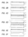
- a first single-crystal substrate member 11 such as an Si wafer
- at least a first layer 12 is formed on a main surface thereof.
- at least a second layer 13 is formed at least on the first layer 12.
- the second layer 13 can be arbitrarily selected from a single-crystal Si layer, a polycrystalline Si layer, an amorphous Si layer, a layer of which a porous surface layer is made non-porous, a metal film, a compound semiconductor film, a superconductive film and the like.
- a device structure such as a MOSFET may be formed in such layer or film.
- the second layer having a multi-layered structure there can be obtained an SOI structure having a buried layer.
- An insulating layer 14 such as of SiO 2 is formed on the outermost layer of the second layer 13, in order to make the potential level of the bonding interface distant from an active layer. Then, as shown in Fig. 2C, the surface of a second substrate member 15 is bonded to the surface of the layer 14 of the first substrate member at the room temperature.
- the bonding is preferably conducted after oxidized Si is formed for example by thermal oxidation on the surface of such single-crystal Si.
- the second substrate member can be selected, for example, from an Si substrate, an Si substrate having an oxidized Si film thereon, a light-transmissive substrate such as quartz, a sapphire substrate and the like, but these examples are not restrictive and any substrate having a sufficiently smooth bonding surface may be employed.
- 2C shows a state in which the second substrate member is bonded to the first substrate member via the insulating layer 14 formed on the surface of the first substrate member, but the insulating layer 14 may be omitted in case of the second layer 13 being not composed of Si or of the second substrate member being not composed of Si.
- the bonding may be conducted by using three members, namely by interposing an insulating member between the first substrate member 11 and the second substrate member 15.
- a heat treatment is then applied in order to increase the bonding strength.
- the two substrate members are separated by the interface of the first layer 12 and the second layer 13.
- a latent factor constituting a separation layer at the interface between the first layer 12 and the second layer 13 or in the vicinity thereof.
- the examples of the factor defining the separation layer include, as described in the foregoing, a variation in the porosity or in the pore size resulting from the anodizing conditions or the subsequent heat treatment, a difference in the thermal expansion coefficient between two different materials, and introduction of an element, a defect layer or a bubble layer by the ion implantation.
- the separation can be achieved, as described in the foregoing, by the application of an external force such as a pressure, a traction, a shear or a wedge force, application of ultrasonic wave or heat, application of an internal pressure to the porous Si by expansion from the periphery of the porous Si due to oxidation of the porous Si, application or a thermal stress by pulsed heating, or by softening, but these are not restrictive.
- an external force such as a pressure, a traction, a shear or a wedge force
- ultrasonic wave or heat application of an internal pressure to the porous Si by expansion from the periphery of the porous Si due to oxidation of the porous Si
- application or a thermal stress by pulsed heating, or by softening but these are not restrictive.
- the semiconductor substrate which is obtained by bonding the second substrate member 15 and the first substrate 14 member 11 via the insulating layer 14, constitutes an SOI substrate adequate for the preparation of isolated electronic devices.
- a surface smoothing treatment such as heat treatment in a non-oxidative atmosphere.
- the first substrate member 11 is used again as the first substrate member 11 or as the second substrate member 15 for the preparation of the SOI substrate, if necessary after the removal of the first layer 12 remaining on the first substrate member and the surface smoothing (cf. Fig. 2F).
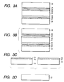
- Figs. 3A to 3D it is also possible, as shown in Figs. 3A to 3D, to use two semiconductor substrate members at the same time, bond two second substrate members to both sides of the first substrate member, employing the steps shown in Figs. 1A to 1D or in Figs. 2A to 2F.
- the first substrate member 21 can be used again as the first substrate member 21 or as the second substrate member 28 (or 29) for the preparation of another SOI substrate, if necessary after the removal of the first layer 22 or 23 remaining on the first substrate member and after the surface smoothing when the surface has unpermissible irregularities.
- the substrate members 28 and 29 need not be of the same material. Also the non-porous films 24, 25 need not be of a same material, and the insulating layers 26 and 27 may be omitted.
- Figs. 4A to 4D show, among the substrate producing methods of the present invention, a method of conducting separation by using a plurality of porous layers.
- a porous region 104 consisting of a first porous layer 102 and a second porous layer 103 of a higher porosity in comparison with the first porous layer 102.
- the porous region may be obtained by making porous the surface portion of a non-porous substrate member or by forming a porous region on the surface of a non-porous substrate member.
- the second porous layer 103 is preferably made thicker than the first porous layer 102.
- the first porous layer 102 is converted into a non-porous layer 102'.
- Such conversion can be achieved, for example, by a heat treatment of the porous layer 102 in a non-oxidative atmosphere.
- the non-oxidative atmosphere is desirably hydrogen-containing atmosphere as described above, and the temperature of the heat treatment is less than the melting point of the material constituting the porous layer, specifically within a range from 600°C to 1400°C, preferably from 900°C to 1200°C.
- the heat treating time is suitably determined according to the porosity and the thickness of the first porous layer so as to convert the first porous layer entirely to a non-porous layer.
- the second porous layer 103 is not converted into a non-porous layer.
- the first substrate 101 is bonded to a second substrate 106, as shown in Fig. 4C, such that the surface of the non-porous layer 102' is in contact with the surface of the second substrate 106, if necessary via another layer 105.
- Such another layer 105 is composed of a material different from that of the layer 102', and may be formed in advance on either of or both of the surfaces of the layer 102' and the second substrate member 106 prior to the ponding.
- the layer 105 may also be omitted when the layer 102' and the second substrate member 106 are of different materials.
- the bonded substrate members 101 and 106 are separated by the application of an external force or by the generation of an internal pressure, whereby the substrate members are mutually divided by the interface between the second porous layer 103 and the non-porous layer 102', which is different from the bonding interface.
- a part of the second porous layer 103 in the vicinity of such separating interface may be broken and lost.
- the separation can be achieved without the porous layer 103 remaining on the separated surface of the layer 102', the second substrate 106 having the layer 102' thereon need not be subjected to selective etching or selective polishing.
- the second substrate 106 having the layer 102' may be heat treated, if necessary, in order to flatten the separated surface of the layer 102'.
- the layer 102' can be formed by epitaxially growing a single-crystal semiconductor layer on the second porous layer 103.
- the layer 102' may be also formed by making the porous layer 102 non-porous and then epitaxially growing a single-crystal semiconductor layer thereon.
- the layer 105 comprises a silicon oxide layer, for example, by oxidizing the surface of the layer 102'.
- this silicon oxide layer is preferably formed as a very thin layer.
- a third porous layer may be formed which has a porosity smaller than that of the second porous layer 103.
- the second porous Si layer formed by using a current density of 50 mA•cm -2 and having a thickness thicker than the first porous layer exhibits a larger porosity and becomes structurally more fragile in comparison with the other porous Si layers.
- the substrate member was then oxidized for 1 hour at 400°C in an oxygen atmosphere, whereby the internal surface of the pores of the porous Si was covered with a thermal oxide film.
- the wafer as the first substrate member was then placed under a hydrogen atmosphere in an epitaxy apparatus, and then was baked for 5 minutes at 1040°C, whereby the pores of the surface region of the porous Si were filled and the outermost first porous Si layer, which was formed with the current density of 1 mA•cm -2 , was converted into non-porous state by the migration of Si atoms.
- an SiO 2 layer of a thickness of 200 nm was formed by thermal oxidation in the surface region of the epitaxially grown Si layer.
- the surface of the SiO 2 layer of the first substrate member was superposed and brought into contact with the surface of another Si substrate member (second substrate member) and heat treatment was conducted for 5 minutes at 1180°C, whereby strong bonding was obtained.
- the bonded substrate members were separated by the application of an external force, whereby the second porous layer of a larger porosity was broken and the division took place at the interface between the non-porous layer and the porous layer.
- the SOI surface is rough, but the substrate in this state is preferably used in the applications in which the surface property is not important, such as in the preparation of a solar cell or micromechanics.
- the substrate in this state is preferably used in the applications in which the surface property is not important, such as in the preparation of a solar cell or micromechanics.
- it is necessary to flatten the surface of the obtained substrate by effecting a heat treatment for example at 1100°C in a non-oxidative atmosphere such as hydrogen.
- the surface roughness after the heat treatment which was evaluated by an atomic force microscope was about 0.2 nm in the root-mean-square in a region of 50 pm square and was equal to that of the commercially available Si wafer.
- the first substrate member was subjected to the selective etching of the remaining porous Si thereon in a mixture of 49% hydrofluoric acid 30% hydrogen peroxide solution under agitation, then to annealing in a hydrogen atmosphere, and was thereafter used again as the first or the second substrate member.
- the third porous layer may also be omitted.
- single-crystal silicon was epitaxially grown with a thickness of 0.3 ⁇ m by CVD under the following growing conditions, on thus formed porous Si without oxidation thereof: Source gas SiH 2 Cl 2 /H 2 gas flow rate 0.5/180 l/min gas pressure 80 Torr temperature 950°C growth rate 0.3 ⁇ m/min.
- an SiO 2 layer of a thickness of 200 nm was formed by thermal oxidation in the surface of the epitaxially grown Si layer.
- the surface of the SiO 2 layer of the first substrate member was superposed and brought into contact with the surface of another Si substrate member (second substrate member) and the bonded substrate members were annealed for 5 minutes at 1180°C, whereby strong bonding was obtained.
- the bonded substrates were separated by the application of an external force, whereby the separation took place immediately under the epitaxial layer.
- the porous Si layer when after anodization the porous Si layer is subjected to the process of epitaxial growth, oxidation, bonding and high-temperature treatment without low-temperature oxidation, it undergoes a structural change, whereby the small pores obtained by the anodization coagulate mutually to expand the pore size. Since such pore expansion immediately under the epitaxial layer causes the strain between the porous Si layer and the epitaxial Si layer, the separation takes place at the interface therebetween by the strain.
- the SOI surface is rough, but the obtained substrate in this state is preferably used in the applications in which the surface property is not important, such as in the production of a solar cell or micromechanics.
- a heat treatment at 1100°C in a hydrogen atmosphere.
- the surface roughness which was evaluated by an atomic force microscope was about 0.2 nm in the root-mean-square in a region of 50 ⁇ m square and was equal to that of the commercially available Si wafer.
- the first substrate member was subjected to the selective etching of the remaining porous Si in a mixture of 49% hydrofluoric acid 30% hydrogen peroxide solution under agitation, thereby removing porous Si, and then to surface polishing, whereby the obtained substrate member could thereafter be used again as the first or the second substrate member.
- the substrate member was oxidized for 1 hour at 400°C in an oxygen atmosphere, whereby the internal surface of the pores in the porous Si was covered with a thermal oxide film.
- single-crystal Si was epitaxially grown with a thickness of 0.15 ⁇ m by CVD under the following growing conditions: Source gas SiH 2 Cl 2 /H 2 gas flow rate 0.5/180 l/min gas pressure 80 Torr temperature 950°C growth rate 0.3 ⁇ m/min.
- an SiO 2 layer of a thickness of 100 nm was formed by thermal oxidation in the surface region of the epitaxially grown Si layer.
- Hydrogen ion implantation was conducted from the surface of the wafer as the first substrate member in such a manner that the projected stroke reaches the vicinity of the porous Si/epitaxial Si interface.
- the ions to be implanted are not respective but can be of any element that can generate a separation layer such as an implantation damaged layer, a high concentration layer of the implanted element (strain layer) or a bubble layer at the interface.
- the surface of the SiO 2 layer of the first substrate member was superposed and brought into contact with the surface of another Si substrate member (second substrate member) and was annealed for 5 minutes, whereby strong bonding was obtained.
- the annealing is conducted under such condition that the implantation damaged layer, the high concentration layer of the implanted element (strain layer) or the bubble layer does not diffuse, and such layer constitute a separation layer.
- the bonded substrate members were separated by the application of an external force, whereby the separation took place at the interface of the porous Si layer and the epitaxial Si layer.
- the surface roughness evaluated by an atomic force microscope was about 0.2 nm in the root-mean-square in a region of 50 ⁇ m square and was equal to that of the commercially available Si wafer.
- the first substrate member was subjected to the removal of the remaining porous Si by selective etching in a mixture of 49% hydrofluoric acid 30% hydrogen peroxide solution under agitation, and could thereafter be reused as the first or the second substrate member.
- the substrate member was oxidized for 1 hour at 400°C in an oxygen atmosphere, whereby the internal surface of the pores in the porous Si was covered with a thermal oxide film. Then the oxide film in the surface portion of the porous Si layer was removed with HF. Thus the internal walls of the pores in the surface portion of the porous Si layer were not covered with the oxide film, but the internal walls of the pores only in the lower portion of the porous Si layer were covered with the oxide film. Then the substrate member was baked for 5 minutes at 1040°C in hydrogen, whereby the surface pores of the porous Si were filled.
- an SiO 2 layer of a thickness of 200 nm was formed by thermal oxidation in the surface region of the epitaxially grown Si layer.
- the surface of the SiO 2 layer of the first substrate member was superposed and brought into contact with the surface of another Si substrate member (second substrate member) and was annealed for 5 minutes at 1180°C, whereby strong bonding was obtained.
- the bonded substrate members were separated by the application of an external force, whereby the division took place immediately under the p - epitaxial layer.
- the substrate member was subjected to a heat treatment for 1 hour at 1100°C in hydrogen.
- the surface coarseness evaluated thereafter by an atomic force microscope was about 0.2 nm in the averaged square coarseness in a region of 50 pm square and was equal to that of the commercially available Si wafer.
- the first substrate member was subjected to the surface polishing of the remaining porous Si, and could thereafter be reused as the first or the second substrate member.
- the substrate member was oxidized for 1 hour at 400°C in an oxygen atmosphere, whereby the internal surface of the pores in the porous Si was covered with a thermal oxide film. Then the thermal oxide film in the surface portion of the porous Si was removed with HF. Then the wafer as the first substrate member was placed in an epitaxy apparatus and was baked for 5 minutes at 1040°C in hydrogen to fill the pores on the surface side of the porous Si.
- MOCVD metal organic chemical vapor deposition
- the surface of the GaAs layer of the first substrate member was superposed and brought into contact with the surface of another Si substrate member (second substrate member) and was annealed for 1 hour at 700°C, whereby strong bonding was obtained.
- the bonding substrate members were separated by the application of an external force, whereby the division took place immediately under the GaAs epitaxial layer.
- the surface side layer of the porous Si was subjected to removal of the oxide film on the pore walls with HF during baking in hydrogen prior to the epitaxial growth, the surface side layer lacking the oxide film on the pore wall exhibited pore coagulation and had a lowered mechanical strength, thereby forming a separative layer.
- a surface-oxidized Si substrate member may be used instead of the Si substrate member.
- the bonding may be conducted after the formation of a deposited SiO 2 film on the Si substrate member or on the GaAs film. In such case, the finally obtained substrate is used as GaAs on an insulating substrate member.
- the first substrate member was subjected to selective etching with a mixture of 49% hydrofluoric acid 30% hydrogen peroxide solution under agitation to remove the remaining porous Si on the first substrate member, and could thereafter be used again as the first or the second substrate member.
- single-crystal Ge was epitaxially grown with a thickness of 0.02 ⁇ m by CVD under the following growing conditions: source gas GeH 4 /H 2 gas flow rate 0.1/180 l/min gas pressure 80 Torr temperature 700°C growth rate 0.05 ⁇ m/min.
- single-crystal Si was epitaxially grown with a thickness of 0.5 ⁇ m by CVD under the following growing conditions: source gas SiH 4 Cl 2 /H 2 gas flow rate 0.5/180 l/min gas pressure 80 Torr temperature 950°C growth rate 0.3 ⁇ m/min.
- an SiO 2 layer having a thickness of 200 nm was formed by thermal oxidation in the surface region of the epitaxially grown Si layer.
- the surface of the SiO 2 layer was superposed and brought into contact with the surface of a separate Si substrate member (second substrate member) and was annealed for 5 minutes at 1180°C, whereby strong bonding was obtained.
- the bonded substrate members were separated by the application of an external force, whereby the separation took place at the epitaxial Si/Ge interface.
- defects are introduced into the interface due to a difference in a lattice constant between Si and Ge. Also, if either layer is ultra thin, the defects tend to be introduced into such ultra thin film. Accordingly, in the present example, the defects are introduced into the Ge film. Because of such difference in the lattice constant and introduction of defects, the Si/Ge interface becomes weaker and causes cleavage.
- the first substrate member was subjected to removal of the remaining Ge layer by surface polishing and could be used again as the first or the second substrate member.
- the surface of a first single-crystal Si substrate member was anodized by immersion in HF solution under the following conditions.
- the second porous Si layer formed with a current density of 50 mA•cm -2 having a thickness layer than the first porous layer exhibited a largest porosity and becomes structurally more fragile layer.
- the substrate member was then oxidized for 1 hour at 400°C in an oxygen atmosphere, whereby the internal surface of the pores of the porous Si was covered with a thermal oxide film.
- the wafer as the substrate member was then placed in an epitaxy apparatus, and was baked for 5 minutes at 1040°C in a hydrogen atmosphere, whereby the pores on the surface side of the porous Si were filled.
- the outermost first porous Si layer formed with the current density of 1 mA•cm -2 was converted into non-porous state.
- single-crystal Si was epitaxially grown with a thickness of 0.3 ⁇ m by CVD, under the following growing conditions: source gas SiH 2 Cl 2 /H 2 gas flow rate 0.5/180 l/min gas pressure 80 Torr temperature 950°C growth rate 0.3 ⁇ m/min.
- an SiO 2 layer having a thickness of 200 nm was formed by thermal oxidation in the surface region of the epitaxially grown Si layer.
- a separate quartz substrate member (second substrate member) was surface-treated with N 2 plasma and rinsed with water. Then, the surface of the SiO 2 layer of the first substrate was superposed and brought into contact with the plasma-treated surface of the quartz substrate member, and heat treatment was conducted for 60 minutes at 400°C, whereby strong bonding was obtained.
- the bonded substrate member were separated by the application of an external force, that is, by causing destruction of the layer having a larger porosity immediately under the non-porous Si layer to divide into two substrate members.
- the porous Si layer formed with the current density of 50 mA•cm -2 and provided immediately under the non-porous Si became the layer having highest porosity.
- the surface roughness evaluated by an atomic force microscope was about 0.2 nm in the root-mean-square in a region of 50 ⁇ m square and was equal to that of the commercially available Si wafer.
- the first substrate member was subjected to selective etching with a mixture of 49% hydrofluoric acid and 30% hydrogen peroxide solution under agitation to remove the porous Si remaining on the first substrate member. Then, the first substrate member was subjected to annealing in a hydrogen atmosphere, and could thereafter be used again as the first or the second substrate member.
- the third porous layer may also be omitted.
- the surface of a first single-crystal Si substrate member was anodized by immersion in HF solution under the following conditions.
- Conditions for forming a third porous layer to be formed finally: current density 7 mA•cm -2 anodizing solution HF:H 2 O:C 2 H 5 OH 1:1:1 time 1 min thickness of porous Si 1 ⁇ m.
- the second porous Si layer formed with a current density of 50 mA•cm -2 became thicker than the first porous layer and exhibited a largest porosity, whereby the second porous Si layer becoming structurally fragile.
- the substrate member was then oxidized for 1 hour at 400°C in an oxygen atmosphere, whereby the internal surface of the pores of the porous Si was covered with a thermal oxide film.
- the wafer as the first substrate member was then placed in a hydrogen baking apparatus, and was baked for 5 minutes at 1040°C in a hydrogen atmosphere, whereby the pores on the surface side of the porous Si were filled.
- the outermost first porous Si layer formed with the current density of 1 mA•cm -2 was converted into non-porous state.
- non-porous layer was a single-crystal layer of excellent quality.
- SiO 2 layer having a thickness of 20 nm was formed by thermal oxidation in the surface region of the epitaxially grown Si layer.
- the surface of the SiO 2 layer was superposed and brought into contact with the surface of another Si substrate member (second substrate member) and heat treatment was conducted for 5 minutes at 1180°C, whereby strong bonding was obtained.
- the bonded substrate member were separated by the application of an external force, that is, by causing destruction of the layer having a largest porosity to divide into two substrate members.
- the heat treatment on the surface of porous Si has a function of moving Si atoms, thereby filling the pores on the surface side. Also H 2 removes the surface oxide film and prevents the regeneration thereof (N. Sato et al. J. Electrochem. Soc., Vol. 142, No. 9, 3116 (1996)). In the H 2 baking, the Si atoms constituting the first porous Si layer are consumed for filling the pores, whereby the second porous Si layer formed with the current density of 50 mA•cm -2 and provided immediately under the outermost layer of non-porous single-crystal Si exhibited the highest porosity.
- the surface roughness evaluated by an atomic force microscope was about 0.2 nm in the root-mean-square in a region of 50 pm square and was equal to that of the commercially available Si wafer.
- the first substrate member was, subjected to selective etching with in a mixture of 49% hydrofluoric acid 30% hydrogen peroxide under agitation to remove the porous Si remaining thereon. Then, the first substrate was subjected to annealing in a hydrogen atmosphere and could thereafter be used again as the first or the second substrate member.
- the third porous layer may also be omitted.
- the substrate member was then oxidized for 1 hour at 400°C in an oxygen atmosphere, whereby the internal surface of the pores of the porous Si was covered with a thermal oxide film.
- the wafer as the first substrate member was then placed in an epitaxy apparatus, and was baked for 5 minutes at 1040°C in a hydrogen atmosphere, whereby the pores on the surface side of the porous Si were filled.
- single-crystal silicon was epitaxially grown with a thickness of 0.3 ⁇ m by CVD on thus formed porous Si under the following growing conditions: source gas SiH 2 Cl 2 /H 2 gas flow rate 0.5/180 l/min gas pressure 80 Torr temperature 950°C growth rate 0.3 ⁇ m/min.
- an SiO 2 layer having a thickness of 200 nm was formed by thermal oxidation in the surface region of the epitaxially grown Si layer.
- the surface of the SiO 2 layer was superposed and brought into contact with the surface of another Si substrate member (second substrate member) and was annealed for 5 minutes at 1180°C, whereby strong bonding was obtained.
- the bonded substrate members were separated by the application of an external force to divide them by the thin porous layer.
- a heat treatment was further conducted for 1 hour at 1100°C in a hydrogen atmosphere.
- the surface roughness evaluated by an atomic force microscope was about 0.2 nm in the root-mean-square in a region of 50 ⁇ m square and was equal to that of the commercially available Si wafer.
- the first substrate member with surface roughness was subjected to surface smoothing treatment by hydrogen annealing without etching or polishing, and could thereafter be used again as the first or the second substrate.
- the substrate member was then placed in an epitaxy apparatus without oxidation of the internal surface of the pores in the porous layer and was baked for 5 minutes at 1040°C in a hydrogen atmosphere, whereby the pores on the surface side of the porous Si were filled.
- single-crystal Si was epitaxially grown with a thickness of 0.3 ⁇ m by CVD under the following growing conditions, on thus formed porous Si: source gas SiH 2 Cl 2 /H 2 gas flow rate 0.5/180 l/min gas pressure 80 Torr temperature 950°C growth rate 0.3 ⁇ m/min.
- an SiO 2 layer having a thickness of 200 nm was formed by thermal oxidation in the surface region of the epitaxially grown Si layer.
- the surface of the SiO 2 layer was superposed and brought into contact with the surface of another Si substrate member (second substrate member) and was annealed for 5 minutes at 1180°C, whereby strong bonding was obtained.
- the bonded substrate members were separated by the application of an external force to divide them by the thin portion of the porous layer which remained without being converted into the non-porous state.
- the surface roughness evaluated by an atomic force microscope was about 0.2 nm in the root-mean-square in a region of 50 ⁇ m square and was equal to that of the commercially available Si wafer.
- the surface roughness on the first substrate member was removed by slight surface etching with a mixture of 49% hydrofluoric acid and 30% hydrogen peroxide solution.
- the first substrate was then subjected to hydrogen annealing, and could thereafter be used again as the first or second substrate member.
- the surface of a first substrate member consisting of a single-crystal Si wafer was anodized by immersion in HF solution under the following conditions, thereby making the surface porous.
- the second porous Si layer formed with a current density of 50 mA•cm -2 became thicker than the first porous layer and exhibited a larger porosity, thereby becoming structurally fragile.
- the substrate member was then oxidized for 1 hour at 400°C in an oxygen atmosphere, whereby the internal surface of the pores of the porous Si was covered with a thermal oxide film.
- the wafer was then placed in an epitaxy apparatus, and was baked for 5 minutes at 1040°C in a hydrogen atmosphere, whereby the first porous layer was converted to a non-porous single-crystal Si layer.
- the second porous layer was provided immediately under the non-porous single-crystal Si layer.
- single-crystal Si was epitaxially grown with a thickness of 0.3 ⁇ m by CVD under the following growing conditions, on thus formed non-porous Si: source gas SiH 2 Cl 2 /H 2 gas flow rate 0.5/180 l/min gas pressure 80 Torr temperature 950°C growth rate 0.3 ⁇ m/min.
- an SiO 2 layer having a thickness of 20 nm was formed by thermal oxidation in the surface region of the epitaxially grown Si layer.
- a single-crystal Si wafer was prepared as the second substrate member.
- the surface of the SiO 2 layer on the first substrate was superposed and brought into contact with the Si surface of the second substrate member, and annealing was conducted for 5 minutes at 1180°C, whereby strong bonding was obtained.
- the baking in hydrogen prior to the epitaxial growth causes migration of atoms constituting the first porous Si to fill the pores, thereby forming a non-porous layer which is integrated with the epitaxial layer to form a non-porous single-crystal Si layer.
- a single-crystal Si layer having a thickness of 0.2 ⁇ m on the Si oxide film.
- the thickness of thus formed single-crystal Si layer measured at 100 points over the entire region thereof exhibited a uniformity of 201 ⁇ 4 nm. Since the surface of the non-porous single-crystal Si layer on the second substrate member was rough, a heat treatment was conducted for 1 hour in hydrogen, at 1100°C. The surface roughness evaluated by an atomic force microscope was about 0.2 nm in the root-mean-square in a region of 50 ⁇ m square.
- the surface roughness remaining on the first substrate member was removed by selective etching in a mixture of 49% hydrofluoric acid 30% hydrogen peroxide solution under agitation.
- the first substrate member was then subjected to annealing in a hydrogen atmosphere, and could thereafter be reused as the first or the second substrate member.
- two SOI substrates can be simultaneously produced by using one first substrate member, forming the aforementioned layers on both surfaces of the first substrate member, and bonding two second substrate member to the both surfaces and separating two second substrate members from the bonded members.
- polishing heat treatment or etching is employed in order to remove the porous Si layer remaining on the first substrate member after the separation of the bonded substrate members.
- etching the following selective etching liquids may be employed as an etchant:
- the remaining layer on the separated surface of the second substrate member substantially absent, the selective etching or selective polishing of the separated surface can be omitted and the substrate can be produced inexpensively.
Landscapes
- Recrystallisation Techniques (AREA)
- Element Separation (AREA)
Applications Claiming Priority (2)
| Application Number | Priority Date | Filing Date | Title |
|---|---|---|---|
| JP7351897 | 1997-03-26 | ||
| JP73518/97 | 1997-03-26 |
Publications (2)
| Publication Number | Publication Date |
|---|---|
| EP0867921A2 true EP0867921A2 (de) | 1998-09-30 |
| EP0867921A3 EP0867921A3 (de) | 1999-03-17 |
Family
ID=13520554
Family Applications (1)
| Application Number | Title | Priority Date | Filing Date |
|---|---|---|---|
| EP98302216A Withdrawn EP0867921A3 (de) | 1997-03-26 | 1998-03-24 | Substrat und Verfahren zu dessen Herstellung |
Country Status (8)
| Country | Link |
|---|---|
| US (2) | US6221738B1 (de) |
| EP (1) | EP0867921A3 (de) |
| KR (1) | KR100265539B1 (de) |
| CN (1) | CN1139969C (de) |
| AU (1) | AU744654B2 (de) |
| CA (1) | CA2233096C (de) |
| SG (1) | SG63832A1 (de) |
| TW (1) | TW447127B (de) |
Cited By (10)
| Publication number | Priority date | Publication date | Assignee | Title |
|---|---|---|---|---|
| EP0995227A4 (de) * | 1997-05-12 | 2000-07-05 | Silicon Genesis Corp | Kontrolliertes spaltungsverfahren |
| US6184111B1 (en) | 1998-06-23 | 2001-02-06 | Silicon Genesis Corporation | Pre-semiconductor process implant and post-process film separation |
| WO2002002458A1 (de) * | 2000-07-05 | 2002-01-10 | Robert Bosch Gmbh | Verfahren zur herstellung eines halbleiterbauelements sowie ein nach dem verfahren hergestelltes halbleiterbauelement |
| WO2002047136A3 (en) * | 2000-12-04 | 2003-06-19 | Motorola Inc | A method for producing soi wafers by delamination |
| FR2855909A1 (fr) * | 2003-06-06 | 2004-12-10 | Soitec Silicon On Insulator | Procede d'obtention concomitante d'au moins une paire de structures comprenant au moins une couche utile reportee sur un substrat |
| US6890838B2 (en) | 1997-07-18 | 2005-05-10 | Silicon Genesis Corporation | Gettering technique for wafers made using a controlled cleaving process |
| US7056808B2 (en) | 1999-08-10 | 2006-06-06 | Silicon Genesis Corporation | Cleaving process to fabricate multilayered substrates using low implantation doses |
| US8945331B2 (en) | 2002-05-17 | 2015-02-03 | Semiconductor Energy Laboratory Co., Ltd. | Method of transferring a laminate and method of manufacturing a semiconductor device |
| US8993410B2 (en) | 2006-09-08 | 2015-03-31 | Silicon Genesis Corporation | Substrate cleaving under controlled stress conditions |
| US9362439B2 (en) | 2008-05-07 | 2016-06-07 | Silicon Genesis Corporation | Layer transfer of films utilizing controlled shear region |
Families Citing this family (92)
| Publication number | Priority date | Publication date | Assignee | Title |
|---|---|---|---|---|
| US6159824A (en) | 1997-05-12 | 2000-12-12 | Silicon Genesis Corporation | Silicon-on-silicon wafer bonding process using a thin film blister-separation method |
| US6033974A (en) | 1997-05-12 | 2000-03-07 | Silicon Genesis Corporation | Method for controlled cleaving process |
| US6291313B1 (en) | 1997-05-12 | 2001-09-18 | Silicon Genesis Corporation | Method and device for controlled cleaving process |
| US6306729B1 (en) | 1997-12-26 | 2001-10-23 | Canon Kabushiki Kaisha | Semiconductor article and method of manufacturing the same |
| MY118019A (en) | 1998-02-18 | 2004-08-30 | Canon Kk | Composite member, its separation method, and preparation method of semiconductor substrate by utilization thereof |
| US6423614B1 (en) * | 1998-06-30 | 2002-07-23 | Intel Corporation | Method of delaminating a thin film using non-thermal techniques |
| JP3395661B2 (ja) * | 1998-07-07 | 2003-04-14 | 信越半導体株式会社 | Soiウエーハの製造方法 |
| US7294535B1 (en) * | 1998-07-15 | 2007-11-13 | Semiconductor Energy Laboratory Co., Ltd. | Crystalline semiconductor thin film, method of fabricating the same, semiconductor device, and method of fabricating the same |
| US7153729B1 (en) * | 1998-07-15 | 2006-12-26 | Semiconductor Energy Laboratory Co., Ltd. | Crystalline semiconductor thin film, method of fabricating the same, semiconductor device, and method of fabricating the same |
| US7282398B2 (en) * | 1998-07-17 | 2007-10-16 | Semiconductor Energy Laboratory Co., Ltd. | Crystalline semiconductor thin film, method of fabricating the same, semiconductor device and method of fabricating the same |
| US7084016B1 (en) * | 1998-07-17 | 2006-08-01 | Semiconductor Energy Laboratory Co., Ltd. | Crystalline semiconductor thin film, method of fabricating the same, semiconductor device, and method of fabricating the same |
| US6559036B1 (en) | 1998-08-07 | 2003-05-06 | Semiconductor Energy Laboratory Co., Ltd. | Semiconductor device and method of manufacturing the same |
| US6890827B1 (en) * | 1999-01-13 | 2005-05-10 | Agere Systems Inc. | Method of fabricating a silicon on insulator transistor structure for imbedded DRAM |
| JP4313874B2 (ja) | 1999-02-02 | 2009-08-12 | キヤノン株式会社 | 基板の製造方法 |
| US6664169B1 (en) * | 1999-06-08 | 2003-12-16 | Canon Kabushiki Kaisha | Process for producing semiconductor member, process for producing solar cell, and anodizing apparatus |
| US6263941B1 (en) | 1999-08-10 | 2001-07-24 | Silicon Genesis Corporation | Nozzle for cleaving substrates |
| US6221740B1 (en) | 1999-08-10 | 2001-04-24 | Silicon Genesis Corporation | Substrate cleaving tool and method |
| JP3975634B2 (ja) * | 2000-01-25 | 2007-09-12 | 信越半導体株式会社 | 半導体ウェハの製作法 |
| JP2001237403A (ja) * | 2000-02-21 | 2001-08-31 | Rohm Co Ltd | 半導体装置の製法および超薄型半導体装置 |
| JP2001284622A (ja) | 2000-03-31 | 2001-10-12 | Canon Inc | 半導体部材の製造方法及び太陽電池の製造方法 |
| JP2001291850A (ja) * | 2000-04-10 | 2001-10-19 | Hitachi Cable Ltd | 結晶シリコン薄膜の製造方法 |
| FR2840731B3 (fr) * | 2002-06-11 | 2004-07-30 | Soitec Silicon On Insulator | Procede de fabrication d'un substrat comportant une couche utile en materiau semi-conducteur monocristallin de proprietes ameliorees |
| US8507361B2 (en) | 2000-11-27 | 2013-08-13 | Soitec | Fabrication of substrates with a useful layer of monocrystalline semiconductor material |
| JP2002305293A (ja) * | 2001-04-06 | 2002-10-18 | Canon Inc | 半導体部材の製造方法及び半導体装置の製造方法 |
| TW574753B (en) * | 2001-04-13 | 2004-02-01 | Sony Corp | Manufacturing method of thin film apparatus and semiconductor device |
| US7238622B2 (en) * | 2001-04-17 | 2007-07-03 | California Institute Of Technology | Wafer bonded virtual substrate and method for forming the same |
| US20050026432A1 (en) * | 2001-04-17 | 2005-02-03 | Atwater Harry A. | Wafer bonded epitaxial templates for silicon heterostructures |
| WO2002084725A1 (en) * | 2001-04-17 | 2002-10-24 | California Institute Of Technology | A method of using a germanium layer transfer to si for photovoltaic applications and heterostructure made thereby |
| US7045878B2 (en) | 2001-05-18 | 2006-05-16 | Reveo, Inc. | Selectively bonded thin film layer and substrate layer for processing of useful devices |
| US6956268B2 (en) * | 2001-05-18 | 2005-10-18 | Reveo, Inc. | MEMS and method of manufacturing MEMS |
| KR100456526B1 (ko) * | 2001-05-22 | 2004-11-09 | 삼성전자주식회사 | 식각저지막을 갖는 에스오아이 기판, 그 제조방법, 그위에 제작된 에스오아이 집적회로 및 그것을 사용하여에스오아이 집적회로를 제조하는 방법 |
| US8415208B2 (en) * | 2001-07-16 | 2013-04-09 | Semiconductor Energy Laboratory Co., Ltd. | Semiconductor device and peeling off method and method of manufacturing semiconductor device |
| JP2003109773A (ja) * | 2001-07-27 | 2003-04-11 | Semiconductor Energy Lab Co Ltd | 発光装置、半導体装置およびそれらの作製方法 |
| JP5057619B2 (ja) * | 2001-08-01 | 2012-10-24 | 株式会社半導体エネルギー研究所 | 半導体装置の作製方法 |
| TW554398B (en) * | 2001-08-10 | 2003-09-21 | Semiconductor Energy Lab | Method of peeling off and method of manufacturing semiconductor device |
| TW558743B (en) | 2001-08-22 | 2003-10-21 | Semiconductor Energy Lab | Peeling method and method of manufacturing semiconductor device |
| US6806171B1 (en) | 2001-08-24 | 2004-10-19 | Silicon Wafer Technologies, Inc. | Method of producing a thin layer of crystalline material |
| US7033910B2 (en) * | 2001-09-12 | 2006-04-25 | Reveo, Inc. | Method of fabricating multi layer MEMS and microfluidic devices |
| US7163826B2 (en) * | 2001-09-12 | 2007-01-16 | Reveo, Inc | Method of fabricating multi layer devices on buried oxide layer substrates |
| US20090065471A1 (en) * | 2003-02-10 | 2009-03-12 | Faris Sadeg M | Micro-nozzle, nano-nozzle, manufacturing methods therefor, applications therefor |
| US6875671B2 (en) * | 2001-09-12 | 2005-04-05 | Reveo, Inc. | Method of fabricating vertical integrated circuits |
| JP2003110108A (ja) * | 2001-09-28 | 2003-04-11 | Mitsubishi Electric Corp | 半導体装置の製造方法及びその構造 |
| KR100944886B1 (ko) * | 2001-10-30 | 2010-03-03 | 가부시키가이샤 한도오따이 에네루기 켄큐쇼 | 반도체 장치의 제조 방법 |
| TWI264121B (en) | 2001-11-30 | 2006-10-11 | Semiconductor Energy Lab | A display device, a method of manufacturing a semiconductor device, and a method of manufacturing a display device |
| FR2835097B1 (fr) * | 2002-01-23 | 2005-10-14 | Procede optimise de report d'une couche mince de carbure de silicium sur un substrat d'accueil | |
| US7202139B2 (en) * | 2002-02-07 | 2007-04-10 | Taiwan Semiconductor Manufacturing Company , Ltd. | MOSFET device with a strained channel |
| US6979630B2 (en) * | 2002-08-08 | 2005-12-27 | Isonics Corporation | Method and apparatus for transferring a thin layer of semiconductor material |
| JP4693411B2 (ja) | 2002-10-30 | 2011-06-01 | 株式会社半導体エネルギー研究所 | 半導体装置の作製方法 |
| FR2849269B1 (fr) * | 2002-12-20 | 2005-07-29 | Soitec Silicon On Insulator | Procede de realisation de cavites dans une plaque de silicium |
| JP2004281998A (ja) * | 2003-01-23 | 2004-10-07 | Seiko Epson Corp | トランジスタとその製造方法、電気光学装置、半導体装置並びに電子機器 |
| WO2004068574A1 (de) * | 2003-01-30 | 2004-08-12 | X-Fab Semiconductor Foundries Ag | Soi kontaktstruktur(en) und zugehöriges herstellungsverfahren |
| US20040218133A1 (en) * | 2003-04-30 | 2004-11-04 | Park Jong-Wan | Flexible electro-optical apparatus and method for manufacturing the same |
| US7592239B2 (en) * | 2003-04-30 | 2009-09-22 | Industry University Cooperation Foundation-Hanyang University | Flexible single-crystal film and method of manufacturing the same |
| US7256104B2 (en) * | 2003-05-21 | 2007-08-14 | Canon Kabushiki Kaisha | Substrate manufacturing method and substrate processing apparatus |
| FR2855910B1 (fr) * | 2003-06-06 | 2005-07-15 | Commissariat Energie Atomique | Procede d'obtention d'une couche tres mince par amincissement par auto-portage provoque |
| TWI242232B (en) * | 2003-06-09 | 2005-10-21 | Canon Kk | Semiconductor substrate, semiconductor device, and method of manufacturing the same |
| FR2858875B1 (fr) * | 2003-08-12 | 2006-02-10 | Soitec Silicon On Insulator | Procede de realisation de couches minces de materiau semi-conducteur a partir d'une plaquette donneuse |
| US7279369B2 (en) * | 2003-08-21 | 2007-10-09 | Intel Corporation | Germanium on insulator fabrication via epitaxial germanium bonding |
| US6967167B2 (en) * | 2003-09-30 | 2005-11-22 | International Business Machines Corporation | Silicon dioxide removing method |
| JP2005136383A (ja) * | 2003-10-09 | 2005-05-26 | Canon Inc | 有機半導体素子、その製造方法および有機半導体装置 |
| FR2861497B1 (fr) * | 2003-10-28 | 2006-02-10 | Soitec Silicon On Insulator | Procede de transfert catastrophique d'une couche fine apres co-implantation |
| US7964925B2 (en) * | 2006-10-13 | 2011-06-21 | Hewlett-Packard Development Company, L.P. | Photodiode module and apparatus including multiple photodiode modules |
| US20050132332A1 (en) * | 2003-12-12 | 2005-06-16 | Abhay Sathe | Multi-location coordinated test apparatus |
| WO2005104192A2 (en) * | 2004-04-21 | 2005-11-03 | California Institute Of Technology | A METHOD FOR THE FABRICATION OF GaAs/Si AND RELATED WAFER BONDED VIRTUAL SUBSTRATES |
| US20060021565A1 (en) * | 2004-07-30 | 2006-02-02 | Aonex Technologies, Inc. | GaInP / GaAs / Si triple junction solar cell enabled by wafer bonding and layer transfer |
| US7846759B2 (en) * | 2004-10-21 | 2010-12-07 | Aonex Technologies, Inc. | Multi-junction solar cells and methods of making same using layer transfer and bonding techniques |
| CN1317739C (zh) * | 2004-11-23 | 2007-05-23 | 中国电子科技集团公司第二十四研究所 | 在具有图形的绝缘硅基衬底上制作硅薄膜的方法 |
| DE102004060363B4 (de) * | 2004-12-15 | 2010-12-16 | Austriamicrosystems Ag | Halbleitersubstrat mit pn-Übergang und Verfahren zur Herstellung |
| US10374120B2 (en) * | 2005-02-18 | 2019-08-06 | Koninklijke Philips N.V. | High efficiency solar cells utilizing wafer bonding and layer transfer to integrate non-lattice matched materials |
| TW200707799A (en) * | 2005-04-21 | 2007-02-16 | Aonex Technologies Inc | Bonded intermediate substrate and method of making same |
| JP5042506B2 (ja) * | 2006-02-16 | 2012-10-03 | 信越化学工業株式会社 | 半導体基板の製造方法 |
| US20070243703A1 (en) * | 2006-04-14 | 2007-10-18 | Aonex Technololgies, Inc. | Processes and structures for epitaxial growth on laminate substrates |
| US7459344B2 (en) * | 2006-08-10 | 2008-12-02 | Taiwan Semiconductor Manufacturing Co., Ltd. | Method for forming micromachined structure |
| US7642934B2 (en) * | 2006-11-10 | 2010-01-05 | Research In Motion Limited | Method of mapping a traditional touchtone keypad on a handheld electronic device and associated apparatus |
| US7732301B1 (en) | 2007-04-20 | 2010-06-08 | Pinnington Thomas Henry | Bonded intermediate substrate and method of making same |
| US20090278233A1 (en) * | 2007-07-26 | 2009-11-12 | Pinnington Thomas Henry | Bonded intermediate substrate and method of making same |
| CN100595882C (zh) * | 2007-12-28 | 2010-03-24 | 上海新傲科技股份有限公司 | 以键合减薄制备绝缘体上硅的方法 |
| US7868374B2 (en) * | 2008-02-21 | 2011-01-11 | International Business Machines Corporation | Semitubular metal-oxide-semiconductor field effect transistor |
| US8987115B2 (en) * | 2008-08-21 | 2015-03-24 | Alliance For Sustainable Energy, Llc | Epitaxial growth of silicon for layer transfer |
| US8871610B2 (en) * | 2008-10-02 | 2014-10-28 | Semiconductor Energy Laboratory Co., Ltd. | Method for manufacturing SOI substrate |
| JP5611571B2 (ja) * | 2008-11-27 | 2014-10-22 | 株式会社半導体エネルギー研究所 | 半導体基板の作製方法及び半導体装置の作製方法 |
| DE102009053262A1 (de) * | 2009-11-13 | 2011-05-19 | Institut Für Solarenergieforschung Gmbh | Verfahren zum Bilden von dünnen Halbleiterschichtsubstraten sowie Verfahren zum Herstellen eines Halbleiterbauelements, insbesondere einer Solarzelle, mit einem solchen Halbleiterschichtsubstrat |
| CN101789466B (zh) * | 2010-02-10 | 2011-12-07 | 上海理工大学 | 太阳能电池制作方法 |
| JP5460418B2 (ja) * | 2010-03-29 | 2014-04-02 | オリジン電気株式会社 | 接合部材の製造方法及び接合部材製造装置 |
| RU2469433C1 (ru) * | 2011-07-13 | 2012-12-10 | Юрий Георгиевич Шретер | Способ лазерного отделения эпитаксиальной пленки или слоя эпитаксиальной пленки от ростовой подложки эпитаксиальной полупроводниковой структуры (варианты) |
| CN103021812B (zh) * | 2012-12-20 | 2016-02-17 | 中国科学院上海微系统与信息技术研究所 | 一种ⅲ-ⅴoi结构的制备方法 |
| WO2014129519A1 (en) | 2013-02-20 | 2014-08-28 | Semiconductor Energy Laboratory Co., Ltd. | Peeling method, semiconductor device, and peeling apparatus |
| WO2015087192A1 (en) | 2013-12-12 | 2015-06-18 | Semiconductor Energy Laboratory Co., Ltd. | Peeling method and peeling apparatus |
| WO2016090636A1 (zh) * | 2014-12-12 | 2016-06-16 | 浙江中纳晶微电子科技有限公司 | 一种晶圆临时键合及分离的方法 |
| CN110676205B (zh) * | 2019-09-17 | 2023-01-06 | 中国电子科技集团公司第十一研究所 | 芯片的衬底的多次使用方法及红外探测器 |
| CN110890418B (zh) * | 2019-12-02 | 2021-11-05 | 中国科学院上海微系统与信息技术研究所 | 一种具有双埋氧层的晶体管结构及其制备方法 |
| US11908723B2 (en) * | 2021-12-03 | 2024-02-20 | International Business Machines Corporation | Silicon handler with laser-release layers |
Family Cites Families (28)
| Publication number | Priority date | Publication date | Assignee | Title |
|---|---|---|---|---|
| US4727047A (en) | 1980-04-10 | 1988-02-23 | Massachusetts Institute Of Technology | Method of producing sheets of crystalline material |
| US4445965A (en) | 1980-12-01 | 1984-05-01 | Carnegie-Mellon University | Method for making thin film cadmium telluride and related semiconductors for solar cells |
| US4906594A (en) * | 1987-06-12 | 1990-03-06 | Agency Of Industrial Science And Technology | Surface smoothing method and method of forming SOI substrate using the surface smoothing method |
| JPH01131031A (ja) * | 1987-11-16 | 1989-05-23 | Seiko Epson Corp | ガラス転写体の製造方法 |
| DE3888184D1 (de) | 1988-11-17 | 1994-04-07 | Ibm | Verfahren zur Herstellung von Masken mit Strukturen im Submikrometerbereich. |
| CA1315574C (en) | 1989-02-02 | 1993-04-06 | Aron M. Rosenfeld | Colour change devices incorporating thin anodic films |
| US5750000A (en) | 1990-08-03 | 1998-05-12 | Canon Kabushiki Kaisha | Semiconductor member, and process for preparing same and semiconductor device formed by use of same |
| SG59963A1 (en) | 1990-08-03 | 1999-02-22 | Canon Kk | Semiconductor member and process for preparing semiconductor member |
| US5198371A (en) * | 1990-09-24 | 1993-03-30 | Biota Corp. | Method of making silicon material with enhanced surface mobility by hydrogen ion implantation |
| FR2681472B1 (fr) * | 1991-09-18 | 1993-10-29 | Commissariat Energie Atomique | Procede de fabrication de films minces de materiau semiconducteur. |
| EP0553852B1 (de) * | 1992-01-30 | 2003-08-20 | Canon Kabushiki Kaisha | Verfahren zur Herstellung eines Halbleitersubstrates |
| JP3261685B2 (ja) | 1992-01-31 | 2002-03-04 | キヤノン株式会社 | 半導体素子基体及びその作製方法 |
| DE69331816T2 (de) * | 1992-01-31 | 2002-08-29 | Canon K.K., Tokio/Tokyo | Verfahren zur Herstellung eines Halbleitersubstrats |
| TW330313B (en) * | 1993-12-28 | 1998-04-21 | Canon Kk | A semiconductor substrate and process for producing same |
| JP3257580B2 (ja) | 1994-03-10 | 2002-02-18 | キヤノン株式会社 | 半導体基板の作製方法 |
| JP3293736B2 (ja) | 1996-02-28 | 2002-06-17 | キヤノン株式会社 | 半導体基板の作製方法および貼り合わせ基体 |
| FR2725074B1 (fr) | 1994-09-22 | 1996-12-20 | Commissariat Energie Atomique | Procede de fabrication d'une structure comportant une couche mince semi-conductrice sur un substrat |
| US6107213A (en) | 1996-02-01 | 2000-08-22 | Sony Corporation | Method for making thin film semiconductor |
| JP3381443B2 (ja) | 1995-02-02 | 2003-02-24 | ソニー株式会社 | 基体から半導体層を分離する方法、半導体素子の製造方法およびsoi基板の製造方法 |
| FR2738671B1 (fr) * | 1995-09-13 | 1997-10-10 | Commissariat Energie Atomique | Procede de fabrication de films minces a materiau semiconducteur |
| CN1132223C (zh) | 1995-10-06 | 2003-12-24 | 佳能株式会社 | 半导体衬底及其制造方法 |
| US5710057A (en) | 1996-07-12 | 1998-01-20 | Kenney; Donald M. | SOI fabrication method |
| SG65697A1 (en) | 1996-11-15 | 1999-06-22 | Canon Kk | Process for producing semiconductor article |
| SG55413A1 (en) | 1996-11-15 | 1998-12-21 | Method Of Manufacturing Semico | Method of manufacturing semiconductor article |
| US6054363A (en) | 1996-11-15 | 2000-04-25 | Canon Kabushiki Kaisha | Method of manufacturing semiconductor article |
| EP0849788B1 (de) | 1996-12-18 | 2004-03-10 | Canon Kabushiki Kaisha | Vefahren zum Herstellen eines Halbleiterartikels unter Verwendung eines Substrates mit einer porösen Halbleiterschicht |
| US6143628A (en) | 1997-03-27 | 2000-11-07 | Canon Kabushiki Kaisha | Semiconductor substrate and method of manufacturing the same |
| US6159824A (en) * | 1997-05-12 | 2000-12-12 | Silicon Genesis Corporation | Silicon-on-silicon wafer bonding process using a thin film blister-separation method |
-
1998
- 1998-03-23 CA CA002233096A patent/CA2233096C/en not_active Expired - Fee Related
- 1998-03-23 SG SG1998000596A patent/SG63832A1/en unknown
- 1998-03-24 EP EP98302216A patent/EP0867921A3/de not_active Withdrawn
- 1998-03-24 US US09/046,433 patent/US6221738B1/en not_active Expired - Fee Related
- 1998-03-24 TW TW087104399A patent/TW447127B/zh not_active IP Right Cessation
- 1998-03-25 AU AU59522/98A patent/AU744654B2/en not_active Ceased
- 1998-03-26 CN CNB981096891A patent/CN1139969C/zh not_active Expired - Fee Related
- 1998-03-26 KR KR1019980010434A patent/KR100265539B1/ko not_active Expired - Fee Related
-
2000
- 2000-11-07 US US09/706,877 patent/US6569748B1/en not_active Expired - Fee Related
Cited By (21)
| Publication number | Priority date | Publication date | Assignee | Title |
|---|---|---|---|---|
| EP0995227A4 (de) * | 1997-05-12 | 2000-07-05 | Silicon Genesis Corp | Kontrolliertes spaltungsverfahren |
| US6890838B2 (en) | 1997-07-18 | 2005-05-10 | Silicon Genesis Corporation | Gettering technique for wafers made using a controlled cleaving process |
| US6184111B1 (en) | 1998-06-23 | 2001-02-06 | Silicon Genesis Corporation | Pre-semiconductor process implant and post-process film separation |
| US7056808B2 (en) | 1999-08-10 | 2006-06-06 | Silicon Genesis Corporation | Cleaving process to fabricate multilayered substrates using low implantation doses |
| US7479232B2 (en) | 2000-07-05 | 2009-01-20 | Robert Bosch Gmbh | Method for producing a semiconductor component and a semiconductor component produced according to the method |
| WO2002002458A1 (de) * | 2000-07-05 | 2002-01-10 | Robert Bosch Gmbh | Verfahren zur herstellung eines halbleiterbauelements sowie ein nach dem verfahren hergestelltes halbleiterbauelement |
| US7037438B2 (en) | 2000-07-05 | 2006-05-02 | Robert Bosch Gmbh | Method for production of a semiconductor component and a semiconductor component produced by said method |
| USRE44995E1 (en) | 2000-07-05 | 2014-07-08 | Robert Bosch Gmbh | Method for producing a semiconductor component and a semiconductor component produced according to the method |
| US8123963B2 (en) | 2000-07-05 | 2012-02-28 | Robert Bosch Gmbh | Method for producing a semiconductor component and a semiconductor component produced according to the method |
| KR100859613B1 (ko) * | 2000-07-05 | 2008-09-23 | 로베르트 보쉬 게엠베하 | 반도체 소자의 제조 방법 및 상기 방법에 의하여 제조된 반도체 소자 |
| WO2002047136A3 (en) * | 2000-12-04 | 2003-06-19 | Motorola Inc | A method for producing soi wafers by delamination |
| US8945331B2 (en) | 2002-05-17 | 2015-02-03 | Semiconductor Energy Laboratory Co., Ltd. | Method of transferring a laminate and method of manufacturing a semiconductor device |
| WO2005004232A1 (fr) * | 2003-06-06 | 2005-01-13 | S.O.I.Tec Silicon On Insulator Technologies | Procede d'obtention concomitante d'une paire de substrats recouverts d'une couche utile |
| US7407867B2 (en) | 2003-06-06 | 2008-08-05 | S.O.I.Tec Silicon On Insulator Technologies | Method for concurrently producing at least a pair of semiconductor structures that each include at least one useful layer on a substrate |
| US7115481B2 (en) | 2003-06-06 | 2006-10-03 | S.O.I.Tec Silicon On Insulator Technologies S.A. | Method for concurrently producing at least a pair of semiconductor structures that each include at least one useful layer on a substrate |
| FR2855909A1 (fr) * | 2003-06-06 | 2004-12-10 | Soitec Silicon On Insulator | Procede d'obtention concomitante d'au moins une paire de structures comprenant au moins une couche utile reportee sur un substrat |
| US8993410B2 (en) | 2006-09-08 | 2015-03-31 | Silicon Genesis Corporation | Substrate cleaving under controlled stress conditions |
| US9356181B2 (en) | 2006-09-08 | 2016-05-31 | Silicon Genesis Corporation | Substrate cleaving under controlled stress conditions |
| US9640711B2 (en) | 2006-09-08 | 2017-05-02 | Silicon Genesis Corporation | Substrate cleaving under controlled stress conditions |
| US9362439B2 (en) | 2008-05-07 | 2016-06-07 | Silicon Genesis Corporation | Layer transfer of films utilizing controlled shear region |
| US11444221B2 (en) | 2008-05-07 | 2022-09-13 | Silicon Genesis Corporation | Layer transfer of films utilizing controlled shear region |
Also Published As
| Publication number | Publication date |
|---|---|
| US6569748B1 (en) | 2003-05-27 |
| CN1139969C (zh) | 2004-02-25 |
| AU744654B2 (en) | 2002-02-28 |
| AU5952298A (en) | 1998-10-01 |
| KR100265539B1 (ko) | 2000-09-15 |
| CA2233096A1 (en) | 1998-09-26 |
| TW447127B (en) | 2001-07-21 |
| US6221738B1 (en) | 2001-04-24 |
| SG63832A1 (en) | 1999-03-30 |
| KR19980080687A (ko) | 1998-11-25 |
| CN1206221A (zh) | 1999-01-27 |
| EP0867921A3 (de) | 1999-03-17 |
| CA2233096C (en) | 2003-01-07 |
Similar Documents
| Publication | Publication Date | Title |
|---|---|---|
| CA2233096C (en) | Substrate and production method thereof | |
| US6054363A (en) | Method of manufacturing semiconductor article | |
| US6143628A (en) | Semiconductor substrate and method of manufacturing the same | |
| JP3352340B2 (ja) | 半導体基体とその製造方法 | |
| US6350702B2 (en) | Fabrication process of semiconductor substrate | |
| EP0843345B1 (de) | Verfahren zur Herstellung eines Halbleitergegenstands | |
| EP0843346B1 (de) | Verfahren zur Herstellung eines Halbleitergegenstands | |
| CA2233132C (en) | Semiconductor substrate and process for producing same | |
| KR19980042471A (ko) | 반도체물품의 제조방법 | |
| JP3697052B2 (ja) | 基板の製造方法及び半導体膜の製造方法 | |
| JP3293767B2 (ja) | 半導体部材の製造方法 | |
| JP3754818B2 (ja) | 半導体基板の作製方法 | |
| JP2002118242A (ja) | 半導体部材の製造方法 | |
| JP3293766B2 (ja) | 半導体部材の製造方法 | |
| HK1002571A (en) | Fabrication process of a semiconductor substrate | |
| JPH11135761A (ja) | 半導体基板の作製方法及び貼り合わせ基板及び半導体基板 |
Legal Events
| Date | Code | Title | Description |
|---|---|---|---|
| PUAI | Public reference made under article 153(3) epc to a published international application that has entered the european phase |
Free format text: ORIGINAL CODE: 0009012 |
|
| AK | Designated contracting states |
Kind code of ref document: A2 Designated state(s): AT BE CH DE ES FR GB IT LI NL PT SE |
|
| AX | Request for extension of the european patent |
Free format text: AL;LT;LV;MK;RO;SI |
|
| PUAL | Search report despatched |
Free format text: ORIGINAL CODE: 0009013 |
|
| AK | Designated contracting states |
Kind code of ref document: A3 Designated state(s): AT BE CH DE DK ES FI FR GB GR IE IT LI LU MC NL PT SE |
|
| AX | Request for extension of the european patent |
Free format text: AL;LT;LV;MK;RO;SI |
|
| 17P | Request for examination filed |
Effective date: 19990730 |
|
| AKX | Designation fees paid |
Free format text: AT BE CH DE ES FR GB IT LI NL PT SE |
|
| 17Q | First examination report despatched |
Effective date: 20020207 |
|
| STAA | Information on the status of an ep patent application or granted ep patent |
Free format text: STATUS: THE APPLICATION HAS BEEN WITHDRAWN |
|
| 18W | Application withdrawn |
Effective date: 20060119 |