EP0867952B1 - Verfahren zur Herstellung eines piezoelektrischen Elements - Google Patents
Verfahren zur Herstellung eines piezoelektrischen Elements Download PDFInfo
- Publication number
- EP0867952B1 EP0867952B1 EP19980105408 EP98105408A EP0867952B1 EP 0867952 B1 EP0867952 B1 EP 0867952B1 EP 19980105408 EP19980105408 EP 19980105408 EP 98105408 A EP98105408 A EP 98105408A EP 0867952 B1 EP0867952 B1 EP 0867952B1
- Authority
- EP
- European Patent Office
- Prior art keywords
- film
- sol
- piezoelectric
- pzt film
- pzt
- Prior art date
- Legal status (The legal status is an assumption and is not a legal conclusion. Google has not performed a legal analysis and makes no representation as to the accuracy of the status listed.)
- Expired - Lifetime
Links
- 238000000034 method Methods 0.000 title claims description 16
- 238000010438 heat treatment Methods 0.000 claims description 14
- 239000000758 substrate Substances 0.000 claims description 14
- 229910052719 titanium Inorganic materials 0.000 claims description 13
- 239000000463 material Substances 0.000 claims description 10
- 229910052791 calcium Inorganic materials 0.000 claims description 6
- 229910052746 lanthanum Inorganic materials 0.000 claims description 6
- 229910052749 magnesium Inorganic materials 0.000 claims description 5
- 229910052758 niobium Inorganic materials 0.000 claims description 5
- 229910052726 zirconium Inorganic materials 0.000 claims description 5
- 229910052745 lead Inorganic materials 0.000 claims description 4
- 239000010410 layer Substances 0.000 description 48
- 239000010936 titanium Substances 0.000 description 14
- 238000004528 spin coating Methods 0.000 description 10
- 238000000137 annealing Methods 0.000 description 9
- XUIMIQQOPSSXEZ-UHFFFAOYSA-N Silicon Chemical compound [Si] XUIMIQQOPSSXEZ-UHFFFAOYSA-N 0.000 description 8
- BASFCYQUMIYNBI-UHFFFAOYSA-N platinum Chemical compound [Pt] BASFCYQUMIYNBI-UHFFFAOYSA-N 0.000 description 8
- 229910052710 silicon Inorganic materials 0.000 description 8
- 239000010703 silicon Substances 0.000 description 8
- RTAQQCXQSZGOHL-UHFFFAOYSA-N Titanium Chemical compound [Ti] RTAQQCXQSZGOHL-UHFFFAOYSA-N 0.000 description 7
- 230000000052 comparative effect Effects 0.000 description 7
- 230000007423 decrease Effects 0.000 description 5
- VYPSYNLAJGMNEJ-UHFFFAOYSA-N Silicium dioxide Chemical compound O=[Si]=O VYPSYNLAJGMNEJ-UHFFFAOYSA-N 0.000 description 4
- 238000002425 crystallisation Methods 0.000 description 4
- 230000008025 crystallization Effects 0.000 description 4
- 238000001035 drying Methods 0.000 description 4
- 229910052697 platinum Inorganic materials 0.000 description 4
- 229910052814 silicon oxide Inorganic materials 0.000 description 4
- GWEVSGVZZGPLCZ-UHFFFAOYSA-N Titan oxide Chemical compound O=[Ti]=O GWEVSGVZZGPLCZ-UHFFFAOYSA-N 0.000 description 3
- 230000003247 decreasing effect Effects 0.000 description 3
- 238000004519 manufacturing process Methods 0.000 description 3
- OGIDPMRJRNCKJF-UHFFFAOYSA-N titanium oxide Inorganic materials [Ti]=O OGIDPMRJRNCKJF-UHFFFAOYSA-N 0.000 description 3
- 239000013078 crystal Substances 0.000 description 2
- 150000002500 ions Chemical group 0.000 description 2
- 239000002243 precursor Substances 0.000 description 2
- 238000004151 rapid thermal annealing Methods 0.000 description 2
- 238000004544 sputter deposition Methods 0.000 description 2
- 239000000126 substance Substances 0.000 description 2
- 238000005299 abrasion Methods 0.000 description 1
- QVGXLLKOCUKJST-UHFFFAOYSA-N atomic oxygen Chemical compound [O] QVGXLLKOCUKJST-UHFFFAOYSA-N 0.000 description 1
- 238000005229 chemical vapour deposition Methods 0.000 description 1
- 238000007599 discharging Methods 0.000 description 1
- 230000000694 effects Effects 0.000 description 1
- 230000001771 impaired effect Effects 0.000 description 1
- 239000004615 ingredient Substances 0.000 description 1
- 230000003647 oxidation Effects 0.000 description 1
- 238000007254 oxidation reaction Methods 0.000 description 1
- 229910052760 oxygen Inorganic materials 0.000 description 1
- 239000001301 oxygen Substances 0.000 description 1
- 238000000059 patterning Methods 0.000 description 1
- 238000003980 solgel method Methods 0.000 description 1
- 239000002344 surface layer Substances 0.000 description 1
Images




Classifications
-
- C—CHEMISTRY; METALLURGY
- C23—COATING METALLIC MATERIAL; COATING MATERIAL WITH METALLIC MATERIAL; CHEMICAL SURFACE TREATMENT; DIFFUSION TREATMENT OF METALLIC MATERIAL; COATING BY VACUUM EVAPORATION, BY SPUTTERING, BY ION IMPLANTATION OR BY CHEMICAL VAPOUR DEPOSITION, IN GENERAL; INHIBITING CORROSION OF METALLIC MATERIAL OR INCRUSTATION IN GENERAL
- C23C—COATING METALLIC MATERIAL; COATING MATERIAL WITH METALLIC MATERIAL; SURFACE TREATMENT OF METALLIC MATERIAL BY DIFFUSION INTO THE SURFACE, BY CHEMICAL CONVERSION OR SUBSTITUTION; COATING BY VACUUM EVAPORATION, BY SPUTTERING, BY ION IMPLANTATION OR BY CHEMICAL VAPOUR DEPOSITION, IN GENERAL
- C23C18/00—Chemical coating by decomposition of either liquid compounds or solutions of the coating forming compounds, without leaving reaction products of surface material in the coating; Contact plating
- C23C18/02—Chemical coating by decomposition of either liquid compounds or solutions of the coating forming compounds, without leaving reaction products of surface material in the coating; Contact plating by thermal decomposition
- C23C18/12—Chemical coating by decomposition of either liquid compounds or solutions of the coating forming compounds, without leaving reaction products of surface material in the coating; Contact plating by thermal decomposition characterised by the deposition of inorganic material other than metallic material
- C23C18/125—Process of deposition of the inorganic material
- C23C18/1254—Sol or sol-gel processing
-
- C—CHEMISTRY; METALLURGY
- C23—COATING METALLIC MATERIAL; COATING MATERIAL WITH METALLIC MATERIAL; CHEMICAL SURFACE TREATMENT; DIFFUSION TREATMENT OF METALLIC MATERIAL; COATING BY VACUUM EVAPORATION, BY SPUTTERING, BY ION IMPLANTATION OR BY CHEMICAL VAPOUR DEPOSITION, IN GENERAL; INHIBITING CORROSION OF METALLIC MATERIAL OR INCRUSTATION IN GENERAL
- C23C—COATING METALLIC MATERIAL; COATING MATERIAL WITH METALLIC MATERIAL; SURFACE TREATMENT OF METALLIC MATERIAL BY DIFFUSION INTO THE SURFACE, BY CHEMICAL CONVERSION OR SUBSTITUTION; COATING BY VACUUM EVAPORATION, BY SPUTTERING, BY ION IMPLANTATION OR BY CHEMICAL VAPOUR DEPOSITION, IN GENERAL
- C23C18/00—Chemical coating by decomposition of either liquid compounds or solutions of the coating forming compounds, without leaving reaction products of surface material in the coating; Contact plating
- C23C18/02—Chemical coating by decomposition of either liquid compounds or solutions of the coating forming compounds, without leaving reaction products of surface material in the coating; Contact plating by thermal decomposition
- C23C18/12—Chemical coating by decomposition of either liquid compounds or solutions of the coating forming compounds, without leaving reaction products of surface material in the coating; Contact plating by thermal decomposition characterised by the deposition of inorganic material other than metallic material
- C23C18/1204—Chemical coating by decomposition of either liquid compounds or solutions of the coating forming compounds, without leaving reaction products of surface material in the coating; Contact plating by thermal decomposition characterised by the deposition of inorganic material other than metallic material inorganic material, e.g. non-oxide and non-metallic such as sulfides, nitrides based compounds
- C23C18/1208—Oxides, e.g. ceramics
- C23C18/1216—Metal oxides
-
- C—CHEMISTRY; METALLURGY
- C23—COATING METALLIC MATERIAL; COATING MATERIAL WITH METALLIC MATERIAL; CHEMICAL SURFACE TREATMENT; DIFFUSION TREATMENT OF METALLIC MATERIAL; COATING BY VACUUM EVAPORATION, BY SPUTTERING, BY ION IMPLANTATION OR BY CHEMICAL VAPOUR DEPOSITION, IN GENERAL; INHIBITING CORROSION OF METALLIC MATERIAL OR INCRUSTATION IN GENERAL
- C23C—COATING METALLIC MATERIAL; COATING MATERIAL WITH METALLIC MATERIAL; SURFACE TREATMENT OF METALLIC MATERIAL BY DIFFUSION INTO THE SURFACE, BY CHEMICAL CONVERSION OR SUBSTITUTION; COATING BY VACUUM EVAPORATION, BY SPUTTERING, BY ION IMPLANTATION OR BY CHEMICAL VAPOUR DEPOSITION, IN GENERAL
- C23C18/00—Chemical coating by decomposition of either liquid compounds or solutions of the coating forming compounds, without leaving reaction products of surface material in the coating; Contact plating
- C23C18/02—Chemical coating by decomposition of either liquid compounds or solutions of the coating forming compounds, without leaving reaction products of surface material in the coating; Contact plating by thermal decomposition
- C23C18/12—Chemical coating by decomposition of either liquid compounds or solutions of the coating forming compounds, without leaving reaction products of surface material in the coating; Contact plating by thermal decomposition characterised by the deposition of inorganic material other than metallic material
- C23C18/1225—Deposition of multilayers of inorganic material
-
- H—ELECTRICITY
- H10—SEMICONDUCTOR DEVICES; ELECTRIC SOLID-STATE DEVICES NOT OTHERWISE PROVIDED FOR
- H10N—ELECTRIC SOLID-STATE DEVICES NOT OTHERWISE PROVIDED FOR
- H10N30/00—Piezoelectric or electrostrictive devices
- H10N30/01—Manufacture or treatment
- H10N30/07—Forming of piezoelectric or electrostrictive parts or bodies on an electrical element or another base
- H10N30/074—Forming of piezoelectric or electrostrictive parts or bodies on an electrical element or another base by depositing piezoelectric or electrostrictive layers, e.g. aerosol or screen printing
- H10N30/077—Forming of piezoelectric or electrostrictive parts or bodies on an electrical element or another base by depositing piezoelectric or electrostrictive layers, e.g. aerosol or screen printing by liquid phase deposition
- H10N30/078—Forming of piezoelectric or electrostrictive parts or bodies on an electrical element or another base by depositing piezoelectric or electrostrictive layers, e.g. aerosol or screen printing by liquid phase deposition by sol-gel deposition
-
- H—ELECTRICITY
- H10—SEMICONDUCTOR DEVICES; ELECTRIC SOLID-STATE DEVICES NOT OTHERWISE PROVIDED FOR
- H10N—ELECTRIC SOLID-STATE DEVICES NOT OTHERWISE PROVIDED FOR
- H10N30/00—Piezoelectric or electrostrictive devices
- H10N30/80—Constructional details
- H10N30/85—Piezoelectric or electrostrictive active materials
- H10N30/853—Ceramic compositions
- H10N30/8548—Lead-based oxides
- H10N30/8554—Lead-zirconium titanate [PZT] based
-
- Y—GENERAL TAGGING OF NEW TECHNOLOGICAL DEVELOPMENTS; GENERAL TAGGING OF CROSS-SECTIONAL TECHNOLOGIES SPANNING OVER SEVERAL SECTIONS OF THE IPC; TECHNICAL SUBJECTS COVERED BY FORMER USPC CROSS-REFERENCE ART COLLECTIONS [XRACs] AND DIGESTS
- Y10—TECHNICAL SUBJECTS COVERED BY FORMER USPC
- Y10T—TECHNICAL SUBJECTS COVERED BY FORMER US CLASSIFICATION
- Y10T29/00—Metal working
- Y10T29/42—Piezoelectric device making
Definitions
- the present invention relates to a process for producing a piezoelectric element and more particularly to a piezoelectric element fit for use in converting electric energy to mechanical energy and vice versa in various kinds of equipment such as an actuator, a pressure sensor, a temperature sensor and so forth.
- the piezoelectric film is generally fabricated with Pb(Zr,Ti)O, (hereinafter called "PZT") as the principal component of a three-component system with a third component added to the two-component PZT.
- PZT Pb(Zr,Ti)O
- the piezoelectric film having such a composition may be formed through a sputtering, sol-gel, laser abrasion, or CVD method.
- a piezoelectric film (PZT film) is required to be about 0.5 ⁇ m 20 ⁇ m thick, for example, and is also required to have a high piezoelectric distortion constant.
- the film has to be annealed (heat-treated) at about 600°C - 700°C to attain the growth of crystalline grains in the piezoelectric film.
- the sol of the PZT film is subjected to spin-coating for drying and pyrolyzing purposes in several cycles. Then, the products are subjected to pre-annealing as a first step. The sol is further subjected to spin-coating for drying and pyrolyzing purposes in several cycles, and then the products are subjected to annealing as a second step.
- the PZT film is usually formed by the use of sols having the same composition for the whole layer.
- An object of the present invention is to solve the foregoing problems by providing a piezoelectric element with improved piezoelectric and dielectric characteristics and a method of producing such a piezoelectric element which does not degrade the withstand voltage of the film.
- the piezoelectric film can further be built up by forming a film on the heat-treated film by applying the first sol at least once, forming a film on the film coated with the first sol by applying the second sol, and subjecting both the films to heat treatment at a predetermined temperature.
- x 1 is set to 100%, the difference in the existing quantity of lead along the thickness of the film is 44% or less.
- the piezoelectric film has a Perovskite structure.
- the piezoelectric and dielectric characteristics are both improved as lead uniformly exists in the piezoelectric film as compared with the conventional film.
- the A x B y O 3 may comprise Pb, La or Ca or a combination thereof as A, and Ti, Zr, Mg or Nb or a combination thereof as B.
- a partial component of the B site or its oxide may be used for the lower electrode as an adhesion layer with respect to the substrate.
- the content of material constituting the A site of the first sol may exceed the content of material constituting the A site of the second sol, but the A site content of the first sol should be less than 1.4 times that of the second sol.
- An exemplary range for the A site of the first sol relative to the A site of the second sol is 1.3 - 1.4, inclusive.
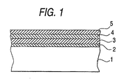
- a piezoelectric element As shown in Fig. 1, a piezoelectric element according to an example helpful for understanding the present invention comprises a silicon substrate 1 (film thickness: about 220 ⁇ m), a silicon oxide film 2 (film thickness: about 1 ⁇ m), a lower electrode 3 (film thickness: about 0.7 ⁇ m), a PZT film 4 (film thickness: about 1 ⁇ m), and an upper electrode 5 (film thickness: about 0.2 ⁇ m). These layers are laid up on the silicon substrate 1 in the aforesaid order.
- the lower electrode 3 has a multilayer structure (not shown) comprising a titanium layer (film thickness: about 0.025 ⁇ m), a titanium oxide layer (film thickness: about 0.02 ⁇ m), a titanium layer (film thickness: about 0.005 ⁇ m), a platinum layer (film thickness: about 0.65 ⁇ m), and a titanium layer (film thickness: about 0.005 ⁇ m) in order as viewed from the silicon substrate 1.
- the quantity of lead along the thickness direction of the PZT film 4 has a difference of 44% or less, providing a fairly uniform lead content throughout the film.
- the PZT film 4 may have a Perovskite structure.
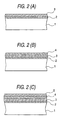
- This piezoelectric element is manufactured through the steps shown in Figs. 2(A)-(C) and 3(A)-(C).
- Figs 3(A)-(C) do not show a process according to the present invention but are helpful for understanding the same. A detailed description will subsequently be given of the process steps.
- the silicon oxide film 2 about 1 ⁇ m thick is formed by thermal oxidation on the silicon substrate 1, which is 2(A)-(C) and about 220 ⁇ m thick.
- the lower electrode 3 is formed on the silicon oxide film 2 through the sputtering method.
- the lower electrode has a multilayer structure (not shown) comprising a titanium layer (film thickness:about 0.025 ⁇ m), a titanium oxide layer (film thickness: about 0.02 ⁇ m), a titanium layer (film thickness: about 0.005 ⁇ m), a platinum layer (film thickness: about 0.65 ⁇ m), and a titanium layer (film thickness: about 0.005 ⁇ m) in order as viewed from the silicon substrate 1.
- the PZT film 4 is formed on the lower electrode 3. Since the PZT film 4 is about 1 ⁇ m thick, a plurality of sols for forming the PZT film 4 are individually subjected to spin-coating before being heat-treated.
- a spin-coating machine is used to coat the lower electrode 3 with a first sol for forming the PZT film, and the product is dried at about 180°C before being pyrolyzed at about 400°C in order to form a PZT film 41 which is about 0.1 - 0.15 ⁇ m thick. This cycle is repeated twice so as to form PZT films 42, 43 on the PZT film 41.
- a composition containing lead greater in quantity by 5% than what is contained in a PZT film to be obtained is used as the first sol according to this embodiment of the present invention.
- the lead excessively contained in the PZT film 44 is offset during heat treatment, whereby the quantity of lead contained in the PZT film 44 is prevented from decreasing to a low quantity in comparison with what is contained in the PZT films 41 - 43. Since the quantity of lead excessively contained in the second sol has been adjusted, the optimum quantity of lead is uniformly distributed in the thickness direction of the PZT film 40A as the lower layer.
- Fig. 3(B) steps similar to those taken to form the PZT films 41 - 43 in Fig. 3(A) are followed to form PZT films 45-47 on the PZT film 40A as the lower layer. Then a step similar to what is taken to form the PZT film 44 in Fig. 3(1) is followed to form a PZT film 48 on the PZT film 47. Further, heat treatment is provided at the structure shown in Fig. 3(B). Here, heat treatment is performed at 600°C for five minutes and continuously at 850°C for one minute to form a PZT film 40B as an upper layer.
- the PZT film 40B as the upper layer is uniformly distributed in the thickness direction of the PZT film 40B as the upper layer as was the case of the PZT films of 40A as the lower layer.
- the PZT film 4 including the films 40A as the lower layer and the films of 40B as the upper layer is obtainable (see Fig. 3(C)).
- the upper electrode 5, which is about 0.2 ⁇ m thick, is formed on the PZT film 4. Subsequently, the desired piezoelectric element is obtained through patterning, and other desired processing steps.
- a piezoelectric element (as a comparative example) is formed in accordance with the above-described steps of the present invention except that the PZT films 44 and 48 were formed with the first sol rather than the second sol.
- a SIMS Single Ion Mass Spectrometer
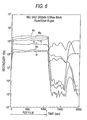
- Fig. 6 shows the results of the SIMS analysis of the product according to the present invention
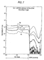
- Fig. 7 shows the SIMS analysis of the comparative example.
- the existing quantity of lead along the thickness of the PZT film according to the present invention is seen to be uniformly distributed.
- the existing quantity of lead is seen to decrease in the proximity of the intermediate portion in the thickness direction of the PZT film 4. More particularly, the lead quantity decreases in the proximity of the boundary between the PZT film formed from the lower layer and the PZT film formed from the upper layer.
- the present invention showed improvement in the piezoelectric constant by about 23% and improvement in the dielectric constant by about 22% without lowering of the withstand voltage.
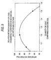
- the piezoelectric constant can be improved by increasing the quantity of lead contained in the second sol by 5% - 47%, preferably 20% - 30% relative to the PZT film that is ultimately to be produced.
- the withstand voltage can be improved by increasing the quantity of lead contained in the second sol by 5% - 43%, preferably 201 - 30% relative to the PZT film that is ultimately to be produced.
- the present invention is not limited to this structure.
- the invention is also applicable to a case where the first sol is applied to the films before they are dried and pyrolyzed in one cycle and then the second sol having a greater lead content than the first sol is applied thereto before they are dried, pyrolyzed and heat-treated at a predetermined temperature.
- the silicon oxide film 2 and the lower electrode 3 are successively formed on the silicon substrate 1 at the step shown in Fig. 10(A).
- a PZT film 14 is formed on the lower electrode 3.
- the PZT film 14 having a thickness of about 1 ⁇ m is formed.
- the first step of applying the first sol for forming the PZT film 14 is taken at least once and the second step of applying the second sol is followed to form the PZT film 14.
- the layers are subjected to heat treatment at predetermined temperatures.
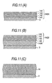
- a piezoelectric film having the Perovskite structure expressed by the general term A x B y O 3 can be used. More specifically, in this Embodiment, Pb, La or Ca is employed as A, whereas Zr 0.52 and Ti 0.48 are employed as B. Further, the first sol is prepared so that the value of x in the general term is 1.3 and the value of y is 1. The second sol is prepared so that the value of x in the general term is 1 and the value of y in the general term is 1.
- the spin-coating machine is used to coat the lower electrode 3 with the first sol for forming the PZT film 14, and the product is dried at about 180°C before being pyrolyzed at about 400°C in order to form a PZT film 141 having a thickness of about 0.1 - 0.15 ⁇ m. This cycle is repeated once again to form a PZT film 142 on the PZT film 141.
- the crystalline growth of the PZT film can be promoted according to the Embodiment of the present invention. Consequently, the whole PZT film can be made with a preferred crystalline orientation.
- the spin-coating machine is used to apply the second sol onto the PZT film 140A as the lower layer formed in Fig. 11(A), and the product is dried at about 180°C before being pyrolyzed at about 400°C in order to form a PZT film 145 which is about 0.1 - 0.15 ⁇ m thick.
- This cycle is repeated three times to form PZT films 146, 147 and 148 on the PZT film 145.
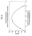
- Fig. 12 shows the results of piezoelectric constants (d31(pC/N)) of piezoelectric elements of this embodiment in comparison with a conventional element.
- the piezoelectric constant of the piezoelectric element according to the present invention (with the value of x exceeding 1 and not greater than 1.4) is seen to have achieved a great deal of improvement in comparison with what has employed the first sol prepared With the value of x at 1 and a value of y at 1 in the general term (the prior art product).
- the invention is not limited to this case but may be applicable to the film resulting from applying the first sol thereto, drying and pyrolyzing it in at least one cycle, again applying the second sol having a greater lead content than the first sol thereto, then drying, pyrolyzing and heat-treating it at predetermined temperatures.
- the processing conditions according to this embodiment of the present invention for example, the film thickness, the heat-treatment temperature, the application of the first and second sols and the like may be varied to the extent that the performance of the piezoelectric element is not impaired.
- the first and second sol have a composition capable of forming a piezoelectric film having the Perovskite crystalline structure and is expressed generally by A x B y O 3 .
- the content of crystallizing precursor material constituting the A site of the first sol is greater than what constitutes the A site of the second sol. Therefore, part of the adhesion layer with respect to the substrate of the lower electrode is diffused in the lower electrode at the time of crystallizing annealing, and the crystallizing precursor material in the proximity of the interface of the lower electrode can be prevented from becoming excessive in the B site. Consequently, the crystal growth in the proximity of the interface of the lower electrode where the crystallization is started at the time of crystallizing annealing is promoted.
- the whole piezoelectric film can be made a columnar film having high orientation and large crystalline grains. Consequently, a piezoelectric element with improved piezoelectric characteristics is producible.
Landscapes
- Chemical & Material Sciences (AREA)
- Engineering & Computer Science (AREA)
- Materials Engineering (AREA)
- Mechanical Engineering (AREA)
- Physics & Mathematics (AREA)
- Thermal Sciences (AREA)
- General Chemical & Material Sciences (AREA)
- Chemical Kinetics & Catalysis (AREA)
- Organic Chemistry (AREA)
- Inorganic Chemistry (AREA)
- Metallurgy (AREA)
- Dispersion Chemistry (AREA)
- Ceramic Engineering (AREA)
- Manufacturing & Machinery (AREA)
- Compositions Of Oxide Ceramics (AREA)
- Particle Formation And Scattering Control In Inkjet Printers (AREA)
- Formation Of Insulating Films (AREA)
- Crystals, And After-Treatments Of Crystals (AREA)
Claims (5)
- Verfahren zum Herstellen eines piezoelektrischen Elements mit einem piezoelektrischen Film (14) sowie einer oberen Elektrode (5) und einer unteren Elektrode (3), zwischen denen der piezoelektrische Film (14) gehalten wird, wobei das Verfahren umfasst:wobei das erste und das zweite Sol eine Zusammensetzung aufweisen, die einen piezoelektrischen Film mit einer Perowskitstruktur bilden kann, die allgemein durch AxByO3 ausgedrückt wird,a) wenigstens einmaliges Auftragen eines ersten Sols für die Verwendung bei der Bildung des piezoelektrischen Films auf einem Substrat (1) mit der darauf ausgebildeten unteren Elektrode (3), um einen unteren Film (141, 142) zu bilden;b) wenigstens einmaliges Auftragen eines zweiten Sols für die Verwendung bei der Bildung des piezoelektrischen Films (14), um einen oberen Film (143, 144) zu bilden, undc) Unterwerfen des oberen und des unteren Films (141, 142, 143, 144) unter eine Wärmebehandlung bei einer vorbestimmten Temperatur nach dem Schritt (b),
wobei der A-Teil aus einer Gruppe gewählt wird, die aus Pb, La und Ca oder einer Kombination aus denselben besteht, und wobei der B-Teil aus einer Gruppe gewählt wird, die aus T, Zr, Mg, Nb oder eine Kombination aus denselben besteht; und
wobei der Anteil des Materials des A-Teils des ersten Sols größer ist als der Anteil des Materials des A-Teils des zweiten Sols. - Verfahren zum Herstellen eines piezoelektrischen Elements nach Anspruch 1, wobei der A-Teil aus Pb besteht.
- Verfahren zum Herstellen eines piezoelektrischen Elements nach Anspruch 1, wobei eine Teilkomponente des B-Teils oder dessen Oxid für die untere Elektrode (3) als eine Haftschicht in Beziehung zu dem Substrat verwendet wird.
- Verfahren zum Herstellen eines piezoelektrischen Elements nach Anspruch 1 oder 2, wobei der Anteil des Materials des A-Teils des ersten Sols den Anteil des Materials des A-Teils des zweiten Sols übersteigt, aber dem 1,4-Fachen oder weniger entspricht.
- Verfahren zum Herstellen eines piezoelektrischen Elements nach Anspruch 4, wobei der Anteil des Materials des A-Teils des ersten Sols dem 1,2 - 1,3-Fachen des Anteils des Materials des A-Teils des zweiten Sols entspricht.
Priority Applications (1)
| Application Number | Priority Date | Filing Date | Title |
|---|---|---|---|
| EP20010114232 EP1179861A3 (de) | 1997-03-27 | 1998-03-25 | Piezoelektrisches Bauelement und dessen Herstellungsverfahren |
Applications Claiming Priority (6)
| Application Number | Priority Date | Filing Date | Title |
|---|---|---|---|
| JP7624697 | 1997-03-27 | ||
| JP76246/97 | 1997-03-27 | ||
| JP7624697 | 1997-03-27 | ||
| JP225156/97 | 1997-08-21 | ||
| JP22515697 | 1997-08-21 | ||
| JP22515697 | 1997-08-21 |
Related Child Applications (1)
| Application Number | Title | Priority Date | Filing Date |
|---|---|---|---|
| EP20010114232 Division EP1179861A3 (de) | 1997-03-27 | 1998-03-25 | Piezoelektrisches Bauelement und dessen Herstellungsverfahren |
Publications (3)
| Publication Number | Publication Date |
|---|---|
| EP0867952A1 EP0867952A1 (de) | 1998-09-30 |
| EP0867952B1 true EP0867952B1 (de) | 2002-09-25 |
| EP0867952B8 EP0867952B8 (de) | 2003-05-28 |
Family
ID=26417405
Family Applications (2)
| Application Number | Title | Priority Date | Filing Date |
|---|---|---|---|
| EP19980105408 Expired - Lifetime EP0867952B8 (de) | 1997-03-27 | 1998-03-25 | Verfahren zur Herstellung eines piezoelektrischen Elements |
| EP20010114232 Withdrawn EP1179861A3 (de) | 1997-03-27 | 1998-03-25 | Piezoelektrisches Bauelement und dessen Herstellungsverfahren |
Family Applications After (1)
| Application Number | Title | Priority Date | Filing Date |
|---|---|---|---|
| EP20010114232 Withdrawn EP1179861A3 (de) | 1997-03-27 | 1998-03-25 | Piezoelektrisches Bauelement und dessen Herstellungsverfahren |
Country Status (4)
| Country | Link |
|---|---|
| US (1) | US6551652B2 (de) |
| EP (2) | EP0867952B8 (de) |
| JP (2) | JP3890733B2 (de) |
| DE (1) | DE69808164T2 (de) |
Families Citing this family (18)
| Publication number | Priority date | Publication date | Assignee | Title |
|---|---|---|---|---|
| US6328433B1 (en) * | 1998-01-22 | 2001-12-11 | Seiko Epson Corporation | Piezoelectric film element and ink-jet recording head using the same |
| JP3948089B2 (ja) * | 1998-01-22 | 2007-07-25 | セイコーエプソン株式会社 | 圧電体素子及びそれを用いたインクジェット式記録ヘッド |
| TW404021B (en) * | 1998-04-09 | 2000-09-01 | Hitachi Ltd | Semiconductor memory device and manufacturing method thereof |
| JP3517876B2 (ja) | 1998-10-14 | 2004-04-12 | セイコーエプソン株式会社 | 強誘電体薄膜素子の製造方法、インクジェット式記録ヘッド及びインクジェットプリンタ |
| JP5115910B2 (ja) * | 2002-01-22 | 2013-01-09 | セイコーエプソン株式会社 | プリンタ |
| JP4530615B2 (ja) | 2002-01-22 | 2010-08-25 | セイコーエプソン株式会社 | 圧電体素子および液体吐出ヘッド |
| US7193756B2 (en) * | 2003-11-26 | 2007-03-20 | Matsushita Electric Industrial Co., Ltd. | Piezoelectric element, method for fabricating the same, inkjet head, method for fabricating the same, and inkjet recording apparatus |
| JP4877451B2 (ja) * | 2004-01-23 | 2012-02-15 | セイコーエプソン株式会社 | 圧電素子の製造方法及び液体噴射ヘッド |
| US20080024563A1 (en) * | 2006-07-25 | 2008-01-31 | Matsushita Electric Industrial Co., Ltd. | Piezoelectric thin film element, ink jet head, and ink jet type recording apparatus |
| US7799158B2 (en) * | 2007-05-28 | 2010-09-21 | Ngk Insulators, Ltd. | Method for producing crystallographically-oriented ceramic |
| JP2011061118A (ja) * | 2009-09-14 | 2011-03-24 | Seiko Epson Corp | 圧電素子、液体噴射ヘッドおよび液体噴射装置 |
| JP5776142B2 (ja) * | 2010-06-25 | 2015-09-09 | コニカミノルタ株式会社 | 振動板 |
| US9705070B2 (en) * | 2010-11-10 | 2017-07-11 | Konica Minolta, Inc. | Ferroelectric thin film, method of manufacturing same and method of manufacturing piezoelectric element |
| JP5892406B2 (ja) | 2011-06-30 | 2016-03-23 | 株式会社リコー | 電気機械変換素子、液滴吐出ヘッド及び液滴吐出装置 |
| JP5954763B2 (ja) * | 2011-12-02 | 2016-07-20 | ローム株式会社 | 圧電体膜、それを用いたセンサおよびアクチュエータ、ならびに圧電体膜の製造方法 |
| JP5539430B2 (ja) * | 2012-03-22 | 2014-07-02 | 富士フイルム株式会社 | 電子機器の製造方法 |
| WO2015114684A1 (ja) * | 2014-01-31 | 2015-08-06 | パナソニックIpマネジメント株式会社 | プロトン伝導体 |
| EP3220430B1 (de) * | 2016-03-16 | 2019-10-30 | Xaar Technology Limited | Piezoelektrisches dünnschichtelement |
Family Cites Families (11)
| Publication number | Priority date | Publication date | Assignee | Title |
|---|---|---|---|---|
| JP2518703B2 (ja) | 1989-11-02 | 1996-07-31 | 堺化学工業株式会社 | 積層型複合圧電体およびその製造方法 |
| US5500988A (en) | 1990-11-20 | 1996-03-26 | Spectra, Inc. | Method of making a perovskite thin-film ink jet transducer |
| GB9025706D0 (en) | 1990-11-27 | 1991-01-09 | Xaar Ltd | Laminate for use in manufacture of ink drop printheads |
| JPH0585704A (ja) * | 1991-03-07 | 1993-04-06 | Olympus Optical Co Ltd | 強誘電体薄膜の製造方法 |
| JP3182909B2 (ja) * | 1991-09-25 | 2001-07-03 | セイコーエプソン株式会社 | 強誘電体キャパシタの製造方法及び強誘電体メモリ装置の製造方法 |
| JP3105081B2 (ja) * | 1992-06-22 | 2000-10-30 | ローム株式会社 | 強誘電体薄膜の製造方法 |
| JPH0620866A (ja) * | 1992-07-02 | 1994-01-28 | Seiko Epson Corp | 誘電体素子 |
| US5502345A (en) | 1994-08-29 | 1996-03-26 | The United States Of America As Represented By The Secretary Of The Navy | Unitary transducer with variable resistivity |
| JPH0867599A (ja) * | 1994-08-30 | 1996-03-12 | Sanyo Electric Co Ltd | 強誘電体薄膜の製造方法 |
| EP0727832B1 (de) * | 1995-02-20 | 2001-11-28 | Seiko Epson Corporation | Verfahren zur Herstellung einer piezoelektrischen Dünnschicht |
| JP3890634B2 (ja) * | 1995-09-19 | 2007-03-07 | セイコーエプソン株式会社 | 圧電体薄膜素子及びインクジェット式記録ヘッド |
-
1998
- 1998-03-25 EP EP19980105408 patent/EP0867952B8/de not_active Expired - Lifetime
- 1998-03-25 DE DE69808164T patent/DE69808164T2/de not_active Expired - Lifetime
- 1998-03-25 EP EP20010114232 patent/EP1179861A3/de not_active Withdrawn
- 1998-03-26 JP JP07912498A patent/JP3890733B2/ja not_active Expired - Fee Related
-
1999
- 1999-11-30 US US09/451,147 patent/US6551652B2/en not_active Expired - Fee Related
-
2006
- 2006-06-15 JP JP2006166232A patent/JP2006245619A/ja not_active Withdrawn
Also Published As
| Publication number | Publication date |
|---|---|
| EP0867952B8 (de) | 2003-05-28 |
| EP1179861A3 (de) | 2003-03-19 |
| EP1179861A2 (de) | 2002-02-13 |
| JP3890733B2 (ja) | 2007-03-07 |
| EP0867952A1 (de) | 1998-09-30 |
| DE69808164T2 (de) | 2003-01-30 |
| US6551652B2 (en) | 2003-04-22 |
| JP2006245619A (ja) | 2006-09-14 |
| DE69808164D1 (de) | 2002-10-31 |
| JPH11126930A (ja) | 1999-05-11 |
| US20020094372A1 (en) | 2002-07-18 |
Similar Documents
| Publication | Publication Date | Title |
|---|---|---|
| EP0867952B1 (de) | Verfahren zur Herstellung eines piezoelektrischen Elements | |
| JP3487068B2 (ja) | 圧電体薄膜およびその製造法ならびにそれを用いたインクジェット記録ヘッド | |
| US7115936B2 (en) | Ferroelectric thin film element and its manufacturing method, thin film capacitor and piezoelectric actuator using same | |
| KR100478748B1 (ko) | 비스무스층구조의강유전성박막형성방법 | |
| JP3666163B2 (ja) | 圧電体素子及びこれを用いたアクチュエータ並びにインクジェット式記録ヘッド | |
| JP2008042069A (ja) | 圧電体素子とその製造方法 | |
| EP1045460A1 (de) | Verfahren zur Herstellung eines piezoelektrischen Elements, piezoelektrisches Element, Tintenstrahldruckkopf und Drucker | |
| JPH10139594A (ja) | 圧電体薄膜およびその製造法ならびにそれを用いたインクジェット記録ヘッド | |
| US6900579B2 (en) | Thin film piezoelectric element | |
| US20060234395A1 (en) | Method for manufacturing perovskite type oxide layer, method for manufacturing ferroelectric memory and method for manufacturing surface acoustic wave element | |
| DE19630110C2 (de) | Schichtaufbau mit einer ferroelektrischen Schicht und Herstellverfahren | |
| JP4144043B2 (ja) | 圧電体薄膜素子の製造方法 | |
| JP4182404B2 (ja) | 強誘電体膜の製膜方法 | |
| JPH0992897A (ja) | 圧電体薄膜素子及びその製造方法、及び圧電体薄膜素子を用いたインクジェット記録ヘッド | |
| CN1064939C (zh) | 压电陶瓷及其制备方法 | |
| JP3389398B2 (ja) | コンデンサ | |
| JP3583638B2 (ja) | 強誘電体キャパシタおよびその製造方法 | |
| JP4029162B2 (ja) | 圧電素子の製造方法 | |
| US8692443B2 (en) | Electrical component comprising a material with a perovskite structure and optimized electrodes and fabrication process | |
| JP2002324924A (ja) | 圧電素子の製造方法 | |
| DE102024115938B4 (de) | Mehrschichtaufbau und Verfahren zur Herstellung eines Mehrschichtaufbaus | |
| Sumi et al. | Effect of the annealing temperature on structural and piezoelectric properties of the sol–gel Pb (Zr0. 56Ti0. 44) 0.90 (Mg1/3Nb2/3) 0.10 O3 films | |
| JP2000346716A (ja) | 圧電体膜 | |
| JPH10219460A (ja) | セラミックス薄膜及びその製造方法 | |
| JP4746161B6 (ja) | 強誘電体層を有する層構造体、および層構造体の製造方法 |
Legal Events
| Date | Code | Title | Description |
|---|---|---|---|
| PUAI | Public reference made under article 153(3) epc to a published international application that has entered the european phase |
Free format text: ORIGINAL CODE: 0009012 |
|
| AK | Designated contracting states |
Kind code of ref document: A1 Designated state(s): DE FR GB IT NL SE |
|
| AX | Request for extension of the european patent |
Free format text: AL;LT;LV;MK;RO;SI |
|
| 17P | Request for examination filed |
Effective date: 19980921 |
|
| AKX | Designation fees paid |
Free format text: DE FR GB IT NL SE |
|
| 17Q | First examination report despatched |
Effective date: 19991230 |
|
| RTI1 | Title (correction) |
Free format text: PROCESS OF PRODUCING A PIEZOELECTRIC ELEMENT |
|
| RTI1 | Title (correction) |
Free format text: PROCESS OF PRODUCING A PIEZOELECTRIC ELEMENT |
|
| RTI1 | Title (correction) |
Free format text: PROCESS OF PRODUCING A PIEZOELECTRIC ELEMENT |
|
| GRAG | Despatch of communication of intention to grant |
Free format text: ORIGINAL CODE: EPIDOS AGRA |
|
| GRAG | Despatch of communication of intention to grant |
Free format text: ORIGINAL CODE: EPIDOS AGRA |
|
| GRAG | Despatch of communication of intention to grant |
Free format text: ORIGINAL CODE: EPIDOS AGRA |
|
| GRAG | Despatch of communication of intention to grant |
Free format text: ORIGINAL CODE: EPIDOS AGRA |
|
| GRAH | Despatch of communication of intention to grant a patent |
Free format text: ORIGINAL CODE: EPIDOS IGRA |
|
| GRAH | Despatch of communication of intention to grant a patent |
Free format text: ORIGINAL CODE: EPIDOS IGRA |
|
| GRAA | (expected) grant |
Free format text: ORIGINAL CODE: 0009210 |
|
| AK | Designated contracting states |
Kind code of ref document: B1 Designated state(s): DE FR GB IT NL SE |
|
| REG | Reference to a national code |
Ref country code: GB Ref legal event code: FG4D |
|
| REF | Corresponds to: |
Ref document number: 69808164 Country of ref document: DE Date of ref document: 20021031 |
|
| ET | Fr: translation filed | ||
| RIN2 | Information on inventor provided after grant (corrected) |
Inventor name: NISHIWAKI, TSUTOMU Inventor name: MURAI, MASAMI Inventor name: SUMI, KOJI Inventor name: KAMEI, HIROYUKI Inventor name: MORIYA, SOICHI Inventor name: QIU, HONG |
|
| PLBE | No opposition filed within time limit |
Free format text: ORIGINAL CODE: 0009261 |
|
| STAA | Information on the status of an ep patent application or granted ep patent |
Free format text: STATUS: NO OPPOSITION FILED WITHIN TIME LIMIT |
|
| 26N | No opposition filed |
Effective date: 20030626 |
|
| PGFP | Annual fee paid to national office [announced via postgrant information from national office to epo] |
Ref country code: SE Payment date: 20110311 Year of fee payment: 14 Ref country code: NL Payment date: 20110321 Year of fee payment: 14 Ref country code: FR Payment date: 20110317 Year of fee payment: 14 Ref country code: IT Payment date: 20110318 Year of fee payment: 14 |
|
| PGFP | Annual fee paid to national office [announced via postgrant information from national office to epo] |
Ref country code: DE Payment date: 20110323 Year of fee payment: 14 Ref country code: GB Payment date: 20110323 Year of fee payment: 14 |
|
| REG | Reference to a national code |
Ref country code: NL Ref legal event code: V1 Effective date: 20121001 |
|
| REG | Reference to a national code |
Ref country code: SE Ref legal event code: EUG |
|
| PG25 | Lapsed in a contracting state [announced via postgrant information from national office to epo] |
Ref country code: SE Free format text: LAPSE BECAUSE OF NON-PAYMENT OF DUE FEES Effective date: 20120326 |
|
| GBPC | Gb: european patent ceased through non-payment of renewal fee |
Effective date: 20120325 |
|
| REG | Reference to a national code |
Ref country code: FR Ref legal event code: ST Effective date: 20121130 |
|
| REG | Reference to a national code |
Ref country code: DE Ref legal event code: R119 Ref document number: 69808164 Country of ref document: DE Effective date: 20121002 |
|
| PG25 | Lapsed in a contracting state [announced via postgrant information from national office to epo] |
Ref country code: GB Free format text: LAPSE BECAUSE OF NON-PAYMENT OF DUE FEES Effective date: 20120325 Ref country code: FR Free format text: LAPSE BECAUSE OF NON-PAYMENT OF DUE FEES Effective date: 20120402 |
|
| PG25 | Lapsed in a contracting state [announced via postgrant information from national office to epo] |
Ref country code: IT Free format text: LAPSE BECAUSE OF NON-PAYMENT OF DUE FEES Effective date: 20120325 |
|
| PG25 | Lapsed in a contracting state [announced via postgrant information from national office to epo] |
Ref country code: NL Free format text: LAPSE BECAUSE OF NON-PAYMENT OF DUE FEES Effective date: 20121001 |
|
| PG25 | Lapsed in a contracting state [announced via postgrant information from national office to epo] |
Ref country code: DE Free format text: LAPSE BECAUSE OF NON-PAYMENT OF DUE FEES Effective date: 20121002 |