EP0868014A1 - Hochspannungsumrichter - Google Patents
Hochspannungsumrichter Download PDFInfo
- Publication number
- EP0868014A1 EP0868014A1 EP98103555A EP98103555A EP0868014A1 EP 0868014 A1 EP0868014 A1 EP 0868014A1 EP 98103555 A EP98103555 A EP 98103555A EP 98103555 A EP98103555 A EP 98103555A EP 0868014 A1 EP0868014 A1 EP 0868014A1
- Authority
- EP
- European Patent Office
- Prior art keywords
- capacitor
- resistor
- power semiconductor
- semiconductor device
- circuit according
- Prior art date
- Legal status (The legal status is an assumption and is not a legal conclusion. Google has not performed a legal analysis and makes no representation as to the accuracy of the status listed.)
- Granted
Links
- 239000003990 capacitor Substances 0.000 claims abstract description 112
- 239000004065 semiconductor Substances 0.000 claims abstract description 91
- 230000003068 static effect Effects 0.000 claims description 10
- 230000000903 blocking effect Effects 0.000 claims description 7
- 238000011144 upstream manufacturing Methods 0.000 claims description 2
- 238000010586 diagram Methods 0.000 description 8
- 230000008901 benefit Effects 0.000 description 7
- 238000006243 chemical reaction Methods 0.000 description 3
- 238000007599 discharging Methods 0.000 description 3
- 230000001276 controlling effect Effects 0.000 description 2
- 230000005540 biological transmission Effects 0.000 description 1
- 230000008859 change Effects 0.000 description 1
- 238000007796 conventional method Methods 0.000 description 1
- 230000001419 dependent effect Effects 0.000 description 1
- 239000000835 fiber Substances 0.000 description 1
- 238000009499 grossing Methods 0.000 description 1
- 238000009413 insulation Methods 0.000 description 1
- 230000001788 irregular Effects 0.000 description 1
- 238000000034 method Methods 0.000 description 1
- 238000012986 modification Methods 0.000 description 1
- 230000004048 modification Effects 0.000 description 1
- 238000010248 power generation Methods 0.000 description 1
- 238000011084 recovery Methods 0.000 description 1
- 230000001105 regulatory effect Effects 0.000 description 1
- 238000010079 rubber tapping Methods 0.000 description 1
- 230000007480 spreading Effects 0.000 description 1
Images


Classifications
-
- H—ELECTRICITY
- H02—GENERATION; CONVERSION OR DISTRIBUTION OF ELECTRIC POWER
- H02M—APPARATUS FOR CONVERSION BETWEEN AC AND AC, BETWEEN AC AND DC, OR BETWEEN DC AND DC, AND FOR USE WITH MAINS OR SIMILAR POWER SUPPLY SYSTEMS; CONVERSION OF DC OR AC INPUT POWER INTO SURGE OUTPUT POWER; CONTROL OR REGULATION THEREOF
- H02M1/00—Details of apparatus for conversion
- H02M1/08—Circuits specially adapted for the generation of control voltages for semiconductor devices incorporated in static converters
- H02M1/088—Circuits specially adapted for the generation of control voltages for semiconductor devices incorporated in static converters for the simultaneous control of series or parallel connected semiconductor devices
- H02M1/096—Circuits specially adapted for the generation of control voltages for semiconductor devices incorporated in static converters for the simultaneous control of series or parallel connected semiconductor devices the power supply of the control circuit being connected in parallel to the main switching element
-
- H—ELECTRICITY
- H02—GENERATION; CONVERSION OR DISTRIBUTION OF ELECTRIC POWER
- H02M—APPARATUS FOR CONVERSION BETWEEN AC AND AC, BETWEEN AC AND DC, OR BETWEEN DC AND DC, AND FOR USE WITH MAINS OR SIMILAR POWER SUPPLY SYSTEMS; CONVERSION OF DC OR AC INPUT POWER INTO SURGE OUTPUT POWER; CONTROL OR REGULATION THEREOF
- H02M1/00—Details of apparatus for conversion
- H02M1/08—Circuits specially adapted for the generation of control voltages for semiconductor devices incorporated in static converters
-
- H—ELECTRICITY
- H03—ELECTRONIC CIRCUITRY
- H03K—PULSE TECHNIQUE
- H03K17/00—Electronic switching or gating, i.e. not by contact-making and –breaking
- H03K17/08—Modifications for protecting switching circuit against overcurrent or overvoltage
- H03K17/081—Modifications for protecting switching circuit against overcurrent or overvoltage without feedback from the output circuit to the control circuit
- H03K17/0814—Modifications for protecting switching circuit against overcurrent or overvoltage without feedback from the output circuit to the control circuit by measures taken in the output circuit
- H03K17/08148—Modifications for protecting switching circuit against overcurrent or overvoltage without feedback from the output circuit to the control circuit by measures taken in the output circuit in composite switches
-
- H—ELECTRICITY
- H02—GENERATION; CONVERSION OR DISTRIBUTION OF ELECTRIC POWER
- H02M—APPARATUS FOR CONVERSION BETWEEN AC AND AC, BETWEEN AC AND DC, OR BETWEEN DC AND DC, AND FOR USE WITH MAINS OR SIMILAR POWER SUPPLY SYSTEMS; CONVERSION OF DC OR AC INPUT POWER INTO SURGE OUTPUT POWER; CONTROL OR REGULATION THEREOF
- H02M1/00—Details of apparatus for conversion
- H02M1/0003—Details of control, feedback or regulation circuits
- H02M1/0006—Arrangements for supplying an adequate voltage to the control circuit of converters
-
- H—ELECTRICITY
- H02—GENERATION; CONVERSION OR DISTRIBUTION OF ELECTRIC POWER
- H02M—APPARATUS FOR CONVERSION BETWEEN AC AND AC, BETWEEN AC AND DC, OR BETWEEN DC AND DC, AND FOR USE WITH MAINS OR SIMILAR POWER SUPPLY SYSTEMS; CONVERSION OF DC OR AC INPUT POWER INTO SURGE OUTPUT POWER; CONTROL OR REGULATION THEREOF
- H02M1/00—Details of apparatus for conversion
- H02M1/08—Circuits specially adapted for the generation of control voltages for semiconductor devices incorporated in static converters
- H02M1/088—Circuits specially adapted for the generation of control voltages for semiconductor devices incorporated in static converters for the simultaneous control of series or parallel connected semiconductor devices
-
- H—ELECTRICITY
- H03—ELECTRONIC CIRCUITRY
- H03K—PULSE TECHNIQUE
- H03K2217/00—Indexing scheme related to electronic switching or gating, i.e. not by contact-making or -breaking covered by H03K17/00
- H03K2217/0036—Means reducing energy consumption
-
- H—ELECTRICITY
- H03—ELECTRONIC CIRCUITRY
- H03K—PULSE TECHNIQUE
- H03K2217/00—Indexing scheme related to electronic switching or gating, i.e. not by contact-making or -breaking covered by H03K17/00
- H03K2217/0081—Power supply means, e.g. to the switch driver
Definitions
- the present invention relates to a high voltage converter circuit comprising a plurality of power semiconductor devices of turn-off type connected in series and for each power semiconductor device a drive unit connected to the gate thereof and adapted to control the power semiconductor device to be turned on and turned off as well as an apparatus for power supply of the drive unit.
- Converter circuit is defined as a circuit being a part of a device for converting high voltage, in which it may be a question of a conversion from direct voltage to alternating voltage or conversely or conversion of direct voltage to direct voltage or alternating voltage to alternating voltage upwardly or downwardly with respect to the voltage level or from one frequency to another.
- Such circuits may for example be used in voltage-stiff converters for transmission of electric power through High Voltage Direct Current (HVDC) for conversion of direct voltage to alternating voltage and conversely.
- Plants for reactive power compensation (RPC) may also utilize such converters.
- These converters may in such plants typically have to hold voltages within the range of 10-500 kV, although also other voltages are conceivable, which makes it necessary to connect comparatively many such power semiconductor devices in series so as to distribute the voltage thereamong, since they normally each may only hold 1-5 kV.
- GTO gate turn-off thyristors
- MOSFETs MOSFETs
- IGBTs Insulated Gate Bipolar Transistors
- the object of the present invention is to provide a high voltage converter circuit of the type defined in the introduction, in which said apparatus for power supply of the drive units is simplier and considerably less expensive than the alternatives described above and still has a very reliable function.
- This object is according to the invention obtained by providing a high voltage converter circuit of the type defined in the introduction, in which the apparatus comprises a first capacitor and a regulator adapted to regulate the voltage across the capacitor, said capacitor and regulator being connected in parallel with the power semiconductor device, the capacitor is adapted to store sufficient electric energy for the power supply of the drive unit when the power semiconductor device is conducting, and the capacitor is connected to the drive unit associated with the power semiconductor device for power supply thereof.
- the first capacitor will in this circuit be able to provide the drive unit with electric energy having the voltage required thereby owing to the fact that the regulator will ensure that the voltage across the capacitor is kept at a desired level.
- the advantage of this type of power supply apparatus is that there is no need for any conventional power supply apparatus utilizing high-insulated transformers. This means a possibility to save costs. Furthermore, the physical size of the apparatus will be small. It is also obtained that the stray capacitance between the drive unit and ground may be low, which is an important advantage in high voltage converter circuits, in which very high voltage time differential coefficients will appear between the drive unit and ground during switching events, which may cause severe EMC problems.
- the regulator is a shunt regulator connected in parallel with the first capacitor
- the apparatus comprises a static voltage divider connected in parallel with the power semiconductor device and having at least a first resistor connected in series with the parallel connection of the shunt regulator and the first capacitor.
- a shunt regulator is defined in a conventional way as a device designed to ensure that the voltage thereacross, and in this case accordingly also across the first capacitor, will not exceed a determined level, and it lets the excess current through.
- a zener diode may for example be used as a shunt regulator, which constitutes another preferred and economi-cally attractive embodiment of the invention.
- the regulator is a series regulator connected in series with the capacitor.
- a series regulator is here in a conventional way defined as a device having a variable resistance adapted to regulate the current therethrough, so that the voltage across the first capacitor is kept substantially constant. It is for true a disadvantage of the use of a series regulator instead of a shunt regulator that this will be considerably more expensive, since it requires a high voltage switch, but it has an advantage in the case of voltages across the power semiconductor device varying strongly, since it would be necessary in the case of a shunt regulator to make the resistor mentioned above very low ohmic so as to obtain a sufficient power supply at low voltages, which results in unreasonably high power losses in the resistor at high voltages.
- the apparatus comprises a DC/DC converter, to the input of which the first capacitor is connected and the outputs of which are connected to the drive unit and adapted to provide the latter with an optional positive and negative voltage.
- a DC/DC converter between the first capacitor and the drive unit is a necessity when the power semiconductor device to be controlled requires the possibility to be able to apply also a negative voltage to the gate thereof which is the case for many power semiconductor devices.
- the efficiency may be raised, by the fact that the input voltage of DC/DC converter is substantially higher than the output voltage, which results in lower power losses in the resistor and the shunt regulator.
- the DC/DC converter is dimensioned so as to at the input thereof utilize voltages having a substantially higher level than required by the drive unit, so that the current consumption from the first capacitor is substantially lower than the total power consumption of the drive unit. It is by this possible to use said converter for obtaining exactly the voltage level demanded by the drive unit without the need for the regulator to ensure that the voltage across the first capacitor is kept at such a low level, whereby the power losses in the apparatus may be kept low.
- a capacitor is connected across each of the outputs of the DC/DC converter so as to store electric energy.
- the drive unit may by this all the time be provided with exactly the voltage required for the moment by tapping voltage across suitable terminals of the capacitors.
- this comprises a second resistor connected in parallel with the shunt regulator and adapted to obtain good voltage division through the static voltage divider at blocking voltages across the power semiconductor device being lower than the limit voltage of the shunt regulator.
- a good voltage division of the apparatus of each power semiconductor device is by this ensured independently of any varying leakage current characteristics between the different power semiconductor devices also at low voltages.
- resistors included in the shunt regulator may also be obtained by resistors included in the shunt regulator.
- the circuit comprises a first diode connected between the terminals of the regulator and the first capacitor being located upstreams with respect to the conducting direction of the power semiconductor device and which diode has the conducting direction towards the first capacitor so as to prevent this capacitor from being discharged otherwise than by the drive unit. This is advantageous for permanently ensure the power supply of the drive unit.
- the apparatus in the embodiment mentioned above having a regulator in the form of a shunt regulator comprises a fourth capacitor connected in parallel with the series connection of the first resistor and the shunt regulator, and the fourth capacitor is adapted to be charged when the power semiconductor device is blocked and discharged through the first resistor and by that charge the first capacitor with electric energy when the power semiconductor device is turned on.
- a charging of and energy storing in the first capacitor is in this way obtained all the time, both at a blocked power semiconductor device and at a turned on one, which makes the power supply of the drive unit very reliable.
- the apparatus comprises a fourth capacitor connected in parallel with the series connection of the series regulator and the first capacitor, and the fourth capacitor is adapted to be charged when the power semiconductor device is blocked and discharged through the series regulator and by that charge the first capacitor with electric energy when the power semiconductor device is turned on.
- a second diode is connected in series with the fourth capacitor and the regulator and prevents the fourth capacitor from being discharged by the power semiconductor device. It is through this prevented that the energy stored in the fourth capacitor is discharged through the power semiconductor device during the conducting state of the semiconductor device.
- the first resistor has a controllable resistance.
- the first resistor is in principle formed by a series regulator.
- the advantage thereof is that the resistance of the resistor may be controlled according to the conditions prevailing so as to keep the power losses low and ensure a safe power supply of the drive unit.
- the resistance of the first resistor may for example be reduced should it be necessary to tap the power required for the drive unit at a low voltage over the power semiconductor device.
- the resistance of the first resistor may then be reduced so as to reduce the voltage over the first capacitor.
- a first resistor is formed by a parallel connection of a fixed resistor and a branch being controllable so as to control the resistance of the first resistor.
- said branch has a resistor with a resistance substantially lower than the resistance of the fixed resistor and a transistor switch connected in series therewith.
- the transistor may be a bipolar transistor, a MOSFET or an IGBT. It will by this be possible to change between two values of the resistance of the first resistor differing substantially according to the conditions prevailing.
- the first resistor is formed by a series connection of a fixed resistor and another resistor as well as a branch connected in parallel with the latter resistor and having a transistor switch arranged controllable to alternatively short-circuit this resistor so as to form the controllable resistance substantially by the resistance of the fixed resistor and disconnect the branch for making the controllable resistance to the sum of the resistance of these both resistors. It is by this obtained that the controllable resistance always gets larger than the resistance of the fixed resistor and that the voltage across the transistor switch may by that not be too high.
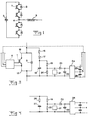
- a phase leg of a high voltage converter circuit, to which the present invention is applicable, is schematically shown in Fig 1.
- the circuit comprises in a conventional way a plurality of power semiconductor devices 1 connected in series, here in the form of IGBTs, and a so-called free-wheeling diode 2 connected in anti-parallel with each such IGBT.
- the number of power semiconductor devices connected in series would in practice be considerably larger than indicated in Fig 1.
- the series connection of the power semiconductor devices is connected to a direct voltage capacitor 3, while the phase terminal 4 between the power semiconductor devices is connected through a phase reactor 5 to for example a phase of an alternating current network.
- the power semiconductor devices with the diodes arranged in Fig 1 above the phase terminal 4 form in this way an IGBT valve and those located thereunder another IGBT valve, in which all the power semiconductor devices in an IGBT valve are turned on simultaneously through signals from a drive unit 6 each schematically indicated in Fig 3, so that the power semiconductor devices in the first IGBT valve are conducting when a positive potential is desired at the phase terminal 4 and the power semiconductor devices in the second IGBT valve are conducting when a negative potential is desired on the phase terminal 4.
- PWM pulse width modulation pattern
- the direct voltage across the direct voltage capacitor 3 may be used for generating a voltage at the phase terminal 4, the fundamental component of which is an alternating voltage having a desired amplitude, frequency and phase position.
- a drive unit for driving an individual power semiconductor device may be structured.
- Each drive unit within an IGBT valve receives simultaneously a control signal, preferably through fibre optic means, for obtaining galvanic insulation and so as to keep the stray capacitance between the power semiconductor device and ground low, at an input 7 from a control apparatus adapted to send control signals according to a desired pattern. It may then be so arranged that upon a logical one at the input 7 a switch 8 is controlled to connect the gate 9 of the IGBT to the positive terminal of a voltage source 10, while an inverter 11 ensures that a second switch 12 receives a logical zero opening it. The gate 9 will then receive a positive voltage with respect to the emitter 13.
- the power semiconductor device is by that turned on. In turning the same off a logical zero is sent to the input 7, in which the switch 8 opens and the switch 12 is closed, so that the gate 9 receives a negative voltage and the IGBT is turned off. This is conventional technique.
- a first resistor 15 connected in series with a second diode 17 and a fourth capacitor 18 is connected between the collector 16 and the emitter 13 of the power semiconductor device in parallel with the power semiconductor device.
- a first resistor 19 is connected in parallel with the fourth capacitor.
- the components described so far constitute a type of static and dynamic voltage divider for power semiconductor devices connected in series, in which the first resistor 19 is then directly connected to the two terminals of the capacitor, and it constitutes a voltage-dividing circuit with the diode 17 as clamping diode, the resistor 15 as current-limiting resistor, the capacitor 18 as clamping capacitor and the resistor 19 as a voltage-diving resistor.
- the diode 17 and the capacitor 18 are used for dynamic voltage division in switches so as to smooth out voltage differences between different IGBTs as a consequence of the spread of the tail current charge when the IGBTs are turned off and the spread in reverse recovery charge when the diode 2 is turned off.
- the resistor 19 is needed both for static voltage division by smoothing out the voltage differences between different IGBTs as a consequence of a spread in leakage current, and for dynamic voltage division by achieving this charging of the capacitor 18 with a time constant T being identical to the resistance of the resistor 19 multiplied by the capacitance of the capacitor 18.
- a parallel connection of a second resistor 20, a shunt regulator 21, such as a zener diode, and a first capacitor 22 are connected in series with the first resistor 19. Between the shunt regulator 21 and the terminal of the first capacitor connected to the mid point between the resistors 19 and 20 a first diode 23 is connected with the conducting direction towards the first capacitor.
- the terminals of the first capacitor 22 are connected to the input of a DC/DC converter 24, which has a second 25 and a third 26 capacitor connected across an output each thereof, wherein + and 0 constitute one output and - and 0 another.
- the terminals of these two capacitors 25, 26 are intended to be connected to the drive unit 6 of the respective power semiconductor device so as to constitute the voltage sources 10 and 14 there.
- the shunt regulator 21 will ensure that the voltage over the capacitor only increases to a limit voltage of for example 300 V, and the first capacitor 22 will be charged and store electric energy at such a blocking. Also the fourth capacitor 18 will be charged. Upon turning on of the power semiconductor device the fourth capacitor 18 will be discharged through the first resistor 19 and in this way contribute to keeping the first capacitor 22 charged. A discharging of the fourth capacitor 18 otherwise than through the first resistor 19 is prevented through the diode 17, while the diode 23 prevents discharging of the first capacitor 22 otherwise than through the DC/DC converter.
- the DC/DC converter is in this way at the input thereof provided with the direct voltage applied across the first capacitor 22, which it converts to a lower direct voltage at the output thereof, so that for example +15 V is obtained at one terminal of the second capacitor 25, 0 V between the terminals of the capacitors and -15 V at the other terminal of the third capacitor 26.
- the capacitors 25, 26 store by this energy which they may supply to the drive unit 6 when this is called for by a control signal 7 at the input thereof, in which the terminals of these capacitors may be imagined to form the voltage source symbols 10 and 14 in Fig 2.
- FIG 4 A part of a high voltage converter circuit according to a second preferred embodiment of the invention is shown in Fig 4, which differs from that shown in Fig 3 by the fact that the third resistor 15 and the second diode 17 are omitted and the second capacitor 18 is replaced by a dynamic voltage divider in the form of a capacitor 27 connected in series with a resistor 28.
- the first resistor 19, the second resistor 20 and the shunt regulator 21 are here functioning as a static voltage divider.
- the first capacitor 22 will in this embodiment only be charged when a high voltage is applied across the power semiconductor device, i.e. when this is in the blocking state.
- the voltage across the first capacitor 22 will decrease below the limit voltage of the shunt regulator when the power semiconductor device is in the turned-on state, in which it is important that the capacitor is made so large with respect to the switching frequency of the power semiconductor device that the voltage across the terminals thereof is not sinking below the level demanded by the DC/DC converter for being able to provide the drive unit with sufficient voltage and current for the proper function thereof.
- FIG. 5 A part of a high voltage converter circuit according to a third preferred embodiment of the invention is schematically illustrated in Fig 5, which only differs from that shown in Fig 3 by the fact that the DC/DC converter 24 and the capacitors 25 and 26 connected thereto have been omitted and the terminals 29, 30 of the first capacitor 22 are connected directly to the drive unit for power supply thereof.
- This embodiment is possible to use in the case in which it is not necessary to provide both negative and positive voltages for the gate of the power semiconductor device and the limit voltage of the shunt regulator may be matched to the desired voltage for the power supply of the drive unit.
- a series regulator 31 is connected in series with a first capacitor 22 in parallel with the power semiconductor device between the collector and the emitter thereof, the terminals of said first capacitor being intended to be connected to a drive unit 6 for power supply thereof.
- the series regulator 31 functions in principle as a variable resistor and regulates the current therethrough, so that the voltage across the capacitor 22 is kept constant. When the power semiconductor device is in the blocking state the capacitor 22 will by this be charged to a desired voltage.
- a static voltage divider with a first resistor 19 connected in parallel with each power semiconductor device.
- This embodiment may of course be supplemented by other components of the other embodiments according to the invention, such as a fourth capacitor, a DC/DC converter and so on, in which the main difference here is that it is a series regulator 31 that ensures a maximum voltage level across the terminals of the first capacitor, while this is ensured through a shun regulator in the first three embodiments.
- the losses of the voltage divider formed by the first resistor and the series connection thereof with the second resistor and a shunt regulator may in some applications be very high. This is especially the case when the drive unit has to be provided with power at very low direct voltages across the power semiconductor device and if the voltage divider has to take care of a large spread in leakage current as a consequence of a large spread of static and dynamic characteristics of the different power semiconductor devices. It is in both these cases important that the first resistor has a very low resistance, which would result in a too high power generation in this resistor when high voltages occur.
- the first resistor has been provided with a variable resistance, i.e.
- a resistor 19' in parallel with a series connection of an additional resistor 32 having a substantially lower resistance than the resistor 19 and a transistor switch 33, which is controllable by a means 34.
- the means 34 may for example react upon voltages across the fourth capacitor 18 and be closed when this voltage exceeds a predetermined value so as to reduce the resistance across the two terminals of the resistor 19' and reduce the voltage across the capacitor.
- the control means 34 may as an alternative react upon a decrease of the voltage across the first capacitor 22 below a determined value and then close the transistor switch 33 so as to be able to deliver sufficient voltage to the DC/DC converter. It should be noticed that the transistor switch 33 should be of a normally on type so as to make the DC/DC converter start.
- a circuit according to another embodiment is shown in Fig 8, this differs from that shown in Fig 7 by the fact that the controllable resistance of the first resistor here is formed by a series connection of a fixed resistor 32' and another resistor 19' as well as a branch connected in parallel with the latter resistor and having a transistor switch 33 controllable through the means 34 to alternatively short-circuit this resistor 19' so as to form the controllable resistance substantially by the resistance of the fixed resistor and interrupt the branch so as to make the controllable resistance to be the sum of the resistances of the two resistors 19', 32'. It is by this obtained that said controllable resistance will never be lower than the resistance of the fixed resistor 32' and the voltage across the transistor switch 33 may never be as high as in the embodiment according to Fig 7.
- Fig 9 differs from that according to Fig 7 by the fact that the series connection of the resistor 32 and the transistor switch 33 has been replaced by a variable current source 35. This is intended to be controlled according to the same principles as the transistor switch 33 in Fig 7.
- the transistor switch 33 may then be controlled according to a suitable PWM method, so that the average of the current discharging the capacitor 18 may be brought to look like for example the line 41.
- the advantage thereof is that we obtain a low differential resistance at a high voltage across the power semiconductor device without making the power consumption in the static voltage divider unnecessarily high.
- Additional components may for example be added to the preferred embodiments shown in the figures and some of them may be removed, such as for example the second resistor, and the circuits may still function under certain conditions.
Landscapes
- Engineering & Computer Science (AREA)
- Power Engineering (AREA)
- Power Conversion In General (AREA)
- Ignition Installations For Internal Combustion Engines (AREA)
Applications Claiming Priority (2)
| Application Number | Priority Date | Filing Date | Title |
|---|---|---|---|
| SE9701070A SE521139C2 (sv) | 1997-03-24 | 1997-03-24 | Högspänningsomriktarkrets |
| SE9701070 | 1997-03-24 |
Publications (2)
| Publication Number | Publication Date |
|---|---|
| EP0868014A1 true EP0868014A1 (de) | 1998-09-30 |
| EP0868014B1 EP0868014B1 (de) | 2008-08-27 |
Family
ID=20406288
Family Applications (1)
| Application Number | Title | Priority Date | Filing Date |
|---|---|---|---|
| EP98103555A Expired - Lifetime EP0868014B1 (de) | 1997-03-24 | 1998-02-28 | Hochspannungsumrichter |
Country Status (6)
| Country | Link |
|---|---|
| US (1) | US5920472A (de) |
| EP (1) | EP0868014B1 (de) |
| JP (1) | JP4070295B2 (de) |
| CA (1) | CA2219343C (de) |
| DE (1) | DE69839932D1 (de) |
| SE (1) | SE521139C2 (de) |
Cited By (10)
| Publication number | Priority date | Publication date | Assignee | Title |
|---|---|---|---|---|
| WO2000054398A1 (en) * | 1999-03-11 | 2000-09-14 | Ericsson, Inc. | General self-driven synchronous rectification scheme for synchronous rectifiers having a floating gate |
| WO2000060730A1 (en) * | 1999-04-07 | 2000-10-12 | Semiconductor Components Industries, L.L.C. | Synchronous rectifier and method of operation |
| WO2002023704A1 (de) * | 2000-09-12 | 2002-03-21 | Siemens Aktiengesellschaft | Schaltungsanordnung zur energieversorgung für eine ansteuerschaltung eines leistungshalbleiterschalters und verfahren zur bereitstellung der ansteuerenergie für einen leistungshalbleiterschalter |
| EP1387474A1 (de) * | 2002-07-30 | 2004-02-04 | Institut National Polytechnique De Grenoble | Versorgungsschaltung für das Schaltelement eines aktiven elektronischen Leistungselementes |
| WO2011095212A3 (en) * | 2010-02-03 | 2011-11-17 | Abb Technology Ag | Switching module to limit and/or break the current of an electric power line |
| US8120391B2 (en) | 2008-09-30 | 2012-02-21 | Infineon Technologies Ag | Circuit arrangement including a voltage supply circuit and semiconductor switching element |
| WO2013091675A1 (en) * | 2011-12-19 | 2013-06-27 | Abb Technology Ltd | Black start of a modular multilevel voltage source converter |
| CN106487043A (zh) * | 2015-08-26 | 2017-03-08 | 国网智能电网研究院 | 一种用于高压直流断路器的混合式一体化高位供能系统 |
| EP3285380A1 (de) * | 2016-08-17 | 2018-02-21 | General Electric Technology GmbH | Spannungsausgleich von spannungsquellenwandlers |
| EP3242390B1 (de) * | 2014-12-29 | 2021-12-15 | Hyosung Heavy Industries Corporation | Leistungsregelungsvorrichtung für ein untermodul eines mmc-wandlers |
Families Citing this family (18)
| Publication number | Priority date | Publication date | Assignee | Title |
|---|---|---|---|---|
| US6515919B1 (en) * | 1998-08-10 | 2003-02-04 | Applied Wireless Identifications Group, Inc. | Radio frequency powered voltage pump for programming EEPROM |
| JP2003070234A (ja) * | 2001-08-28 | 2003-03-07 | Toshiba Corp | 自己消弧型素子のゲート電源装置 |
| US7109603B2 (en) * | 2003-01-16 | 2006-09-19 | Quality Rf Services | Power converter system |
| JP4342251B2 (ja) * | 2003-09-10 | 2009-10-14 | 株式会社東芝 | ゲート駆動回路 |
| JP4726499B2 (ja) * | 2005-01-17 | 2011-07-20 | 東芝三菱電機産業システム株式会社 | 電圧駆動型半導体スイッチング素子の制御装置 |
| CN101588647A (zh) * | 2008-05-19 | 2009-11-25 | 深圳富泰宏精密工业有限公司 | 自动开机装置 |
| DE102009045052B4 (de) | 2008-09-30 | 2013-04-04 | Infineon Technologies Ag | Bereitstellen einer Versorgungsspannung für eine Ansteuerschaltung eines Halbleiterschaltelements |
| JP5638194B2 (ja) * | 2008-11-19 | 2014-12-10 | 東芝三菱電機産業システム株式会社 | 電力用半導体素子のゲート回路 |
| CA2759818C (en) | 2009-05-07 | 2016-11-01 | Abb Technology Ag | Method and arrangement to determine the cell capacitor voltage of a cell of a multi-cell power converter |
| CN102804569A (zh) | 2009-06-16 | 2012-11-28 | 西门子公司 | 与功率开关并联连接的用于功率开关的控制电路的电源 |
| CN103828205B (zh) * | 2011-06-27 | 2016-05-18 | Abb技术有限公司 | 用于控制电力开关的电源 |
| CN105281545B (zh) * | 2015-11-05 | 2019-08-06 | 许继电气股份有限公司 | 一种柔性直流换流阀及其桥臂阻尼模块取能电路 |
| CN105576953A (zh) * | 2016-01-04 | 2016-05-11 | 许继电气股份有限公司 | 一种mmc柔性直流换流阀及其子模块取电电路 |
| GB2565297B (en) * | 2017-08-07 | 2020-09-02 | Murata Manufacturing Co | An adjustable power supply device for supplying power to a power switch control device |
| JP2020177875A (ja) * | 2019-04-23 | 2020-10-29 | 東芝三菱電機産業システム株式会社 | 直流遮断装置 |
| JP7702774B2 (ja) * | 2022-04-18 | 2025-07-04 | 株式会社Tmeic | 電力変換装置 |
| JP7836348B2 (ja) * | 2024-03-25 | 2026-03-26 | シャープ株式会社 | 補助電源回路および電源装置 |
| EP4641907A1 (de) * | 2024-04-24 | 2025-10-29 | Abb Schweiz Ag | Flugkondensator-mehrpegelwandler |
Citations (2)
| Publication number | Priority date | Publication date | Assignee | Title |
|---|---|---|---|---|
| EP0031083A1 (de) * | 1979-12-20 | 1981-07-01 | Asea Ab | Spannungsteilerschaltung zum Anschluss parallel zu einem Thyristor |
| EP0654885A1 (de) * | 1993-11-22 | 1995-05-24 | Gec Alsthom Transport Sa | Stromversorgungsvorrichtung für die Steuerschaltung eines Leistungsschalters |
Family Cites Families (6)
| Publication number | Priority date | Publication date | Assignee | Title |
|---|---|---|---|---|
| CA1313219C (en) * | 1988-10-07 | 1993-01-26 | Boon-Teck Ooi | Pulse width modulation high voltage direct current transmission system and converter |
| US5027264A (en) * | 1989-09-29 | 1991-06-25 | Wisconsin Alumni Research Foundation | Power conversion apparatus for DC/DC conversion using dual active bridges |
| DE4428674B4 (de) * | 1994-08-12 | 2005-08-11 | Siemens Ag | Verfahren zur Steuerung des Abschaltvorgangs eines spannungsgesteuerten, abschaltbaren Leistungshalbleiter-Schalters und Vorrichtung zur Durchführung des Verfahrens |
| US5691632A (en) * | 1995-05-26 | 1997-11-25 | Toko, Inc. | Switching power supply |
| SE9502249D0 (sv) * | 1995-06-21 | 1995-06-21 | Abb Research Ltd | Converter circuitry having at least one switching device and circuit module |
| US5698970A (en) * | 1996-04-16 | 1997-12-16 | Exar Corporation | Switching shunt regulator |
-
1997
- 1997-03-24 SE SE9701070A patent/SE521139C2/sv not_active IP Right Cessation
- 1997-08-29 US US08/921,087 patent/US5920472A/en not_active Expired - Lifetime
- 1997-11-13 CA CA002219343A patent/CA2219343C/en not_active Expired - Lifetime
-
1998
- 1998-02-28 EP EP98103555A patent/EP0868014B1/de not_active Expired - Lifetime
- 1998-02-28 DE DE69839932T patent/DE69839932D1/de not_active Expired - Lifetime
- 1998-03-23 JP JP07461498A patent/JP4070295B2/ja not_active Expired - Lifetime
Patent Citations (2)
| Publication number | Priority date | Publication date | Assignee | Title |
|---|---|---|---|---|
| EP0031083A1 (de) * | 1979-12-20 | 1981-07-01 | Asea Ab | Spannungsteilerschaltung zum Anschluss parallel zu einem Thyristor |
| EP0654885A1 (de) * | 1993-11-22 | 1995-05-24 | Gec Alsthom Transport Sa | Stromversorgungsvorrichtung für die Steuerschaltung eines Leistungsschalters |
Cited By (15)
| Publication number | Priority date | Publication date | Assignee | Title |
|---|---|---|---|---|
| WO2000054398A1 (en) * | 1999-03-11 | 2000-09-14 | Ericsson, Inc. | General self-driven synchronous rectification scheme for synchronous rectifiers having a floating gate |
| WO2000060730A1 (en) * | 1999-04-07 | 2000-10-12 | Semiconductor Components Industries, L.L.C. | Synchronous rectifier and method of operation |
| WO2002023704A1 (de) * | 2000-09-12 | 2002-03-21 | Siemens Aktiengesellschaft | Schaltungsanordnung zur energieversorgung für eine ansteuerschaltung eines leistungshalbleiterschalters und verfahren zur bereitstellung der ansteuerenergie für einen leistungshalbleiterschalter |
| EP1387474A1 (de) * | 2002-07-30 | 2004-02-04 | Institut National Polytechnique De Grenoble | Versorgungsschaltung für das Schaltelement eines aktiven elektronischen Leistungselementes |
| FR2843247A1 (fr) * | 2002-07-30 | 2004-02-06 | Inst Nat Polytech Grenoble | Dispositif d'alimentation d'un element de commande d'un composant electronique de puissance actif. |
| US8120391B2 (en) | 2008-09-30 | 2012-02-21 | Infineon Technologies Ag | Circuit arrangement including a voltage supply circuit and semiconductor switching element |
| US8344764B2 (en) | 2008-09-30 | 2013-01-01 | Infineon Technologies Ag | Circuit arrangement including voltage supply circuit |
| WO2011095212A3 (en) * | 2010-02-03 | 2011-11-17 | Abb Technology Ag | Switching module to limit and/or break the current of an electric power line |
| US9065326B2 (en) | 2010-02-03 | 2015-06-23 | Abb Technology Ltd | Switching module for use in a device to limit and/or break the current of a power transmission or distribution line |
| WO2013091675A1 (en) * | 2011-12-19 | 2013-06-27 | Abb Technology Ltd | Black start of a modular multilevel voltage source converter |
| US9667133B2 (en) | 2011-12-19 | 2017-05-30 | Abb Schweiz Ag | Black start of a multilevel voltage source converter |
| EP3242390B1 (de) * | 2014-12-29 | 2021-12-15 | Hyosung Heavy Industries Corporation | Leistungsregelungsvorrichtung für ein untermodul eines mmc-wandlers |
| CN106487043A (zh) * | 2015-08-26 | 2017-03-08 | 国网智能电网研究院 | 一种用于高压直流断路器的混合式一体化高位供能系统 |
| EP3285380A1 (de) * | 2016-08-17 | 2018-02-21 | General Electric Technology GmbH | Spannungsausgleich von spannungsquellenwandlers |
| WO2018033434A1 (en) * | 2016-08-17 | 2018-02-22 | General Electric Technology Gmbh | Voltage balancing of voltage source converters |
Also Published As
| Publication number | Publication date |
|---|---|
| US5920472A (en) | 1999-07-06 |
| EP0868014B1 (de) | 2008-08-27 |
| SE9701070D0 (sv) | 1997-03-24 |
| SE521139C2 (sv) | 2003-10-07 |
| JP4070295B2 (ja) | 2008-04-02 |
| JPH10271810A (ja) | 1998-10-09 |
| SE9701070L (sv) | 1998-09-25 |
| CA2219343A1 (en) | 1998-09-24 |
| DE69839932D1 (de) | 2008-10-09 |
| CA2219343C (en) | 2003-09-23 |
Similar Documents
| Publication | Publication Date | Title |
|---|---|---|
| EP0868014B1 (de) | Hochspannungsumrichter | |
| US5644482A (en) | HVDC transmission system with multiple converter stations | |
| US9083274B2 (en) | Power stage precharging and dynamic braking apparatus for multilevel inverter | |
| US4706177A (en) | DC-AC inverter with overload driving capability | |
| US5946178A (en) | Protective circuit for series-connected power semiconductors | |
| US5710698A (en) | Delta connected resonant snubber circuit | |
| EP0419230B1 (de) | Dämpferschaltung eines Leistungswandlers | |
| US5347166A (en) | Apparatus and method for switching high power levels | |
| US20120057387A1 (en) | Hybrid switch for resonant power converters | |
| EP1051799A1 (de) | Wandlervorrichtung | |
| CA2620098A1 (en) | Pulse resistor | |
| US7480160B2 (en) | Traction converter having a line-side four-quadrant controller, and method therefor | |
| MX2007014842A (es) | Funcionamiento de un inversor con sobremodulacion. | |
| US6137703A (en) | Clamped bidirectional power switches | |
| EP0079130A1 (de) | Verlustfreier Ausschalt-Entlastungskreis für mit Klemmdioden beschaltete Induktivlast | |
| US6023419A (en) | Capacitor regulated controllable voltage and current power supply | |
| US5400242A (en) | Multi-series inverter arrangement | |
| JPH07111784A (ja) | 電力変換装置 | |
| EP1396926A1 (de) | DC/DC-Wandler mit aktiver Klemmschaltung | |
| US5689410A (en) | Split-boost circuit having imbalance protection circuitry | |
| US3987357A (en) | AC voltage regulator | |
| EP4641907A1 (de) | Flugkondensator-mehrpegelwandler | |
| AU631861B2 (en) | Circuits with switching protection and parts therefor | |
| US20230353043A1 (en) | Switching valve | |
| US5777865A (en) | Power conversion apparatus and its controlling method |
Legal Events
| Date | Code | Title | Description |
|---|---|---|---|
| PUAI | Public reference made under article 153(3) epc to a published international application that has entered the european phase |
Free format text: ORIGINAL CODE: 0009012 |
|
| AK | Designated contracting states |
Kind code of ref document: A1 Designated state(s): DE FR GB IT SE |
|
| AX | Request for extension of the european patent |
Free format text: AL;LT;LV;MK;RO;SI |
|
| 17P | Request for examination filed |
Effective date: 19990312 |
|
| AKX | Designation fees paid |
Free format text: DE FR GB IT SE |
|
| RAP1 | Party data changed (applicant data changed or rights of an application transferred) |
Owner name: ABB AB |
|
| 17Q | First examination report despatched |
Effective date: 20070124 |
|
| GRAP | Despatch of communication of intention to grant a patent |
Free format text: ORIGINAL CODE: EPIDOSNIGR1 |
|
| RIN1 | Information on inventor provided before grant (corrected) |
Inventor name: ZDANSKY, LENNART Inventor name: PERSSON, ANDERS Inventor name: BILJENGA, BO |
|
| GRAS | Grant fee paid |
Free format text: ORIGINAL CODE: EPIDOSNIGR3 |
|
| GRAA | (expected) grant |
Free format text: ORIGINAL CODE: 0009210 |
|
| AK | Designated contracting states |
Kind code of ref document: B1 Designated state(s): DE FR GB IT SE |
|
| REG | Reference to a national code |
Ref country code: GB Ref legal event code: FG4D |
|
| REF | Corresponds to: |
Ref document number: 69839932 Country of ref document: DE Date of ref document: 20081009 Kind code of ref document: P |
|
| PLBE | No opposition filed within time limit |
Free format text: ORIGINAL CODE: 0009261 |
|
| STAA | Information on the status of an ep patent application or granted ep patent |
Free format text: STATUS: NO OPPOSITION FILED WITHIN TIME LIMIT |
|
| 26N | No opposition filed |
Effective date: 20090528 |
|
| PG25 | Lapsed in a contracting state [announced via postgrant information from national office to epo] |
Ref country code: SE Free format text: LAPSE BECAUSE OF FAILURE TO SUBMIT A TRANSLATION OF THE DESCRIPTION OR TO PAY THE FEE WITHIN THE PRESCRIBED TIME-LIMIT Effective date: 20081127 |
|
| REG | Reference to a national code |
Ref country code: FR Ref legal event code: PLFP Year of fee payment: 18 |
|
| REG | Reference to a national code |
Ref country code: FR Ref legal event code: PLFP Year of fee payment: 19 |
|
| REG | Reference to a national code |
Ref country code: FR Ref legal event code: PLFP Year of fee payment: 20 |
|
| PGFP | Annual fee paid to national office [announced via postgrant information from national office to epo] |
Ref country code: FR Payment date: 20170217 Year of fee payment: 20 Ref country code: DE Payment date: 20170217 Year of fee payment: 20 |
|
| PGFP | Annual fee paid to national office [announced via postgrant information from national office to epo] |
Ref country code: GB Payment date: 20170216 Year of fee payment: 20 |
|
| PGFP | Annual fee paid to national office [announced via postgrant information from national office to epo] |
Ref country code: IT Payment date: 20170221 Year of fee payment: 20 |
|
| REG | Reference to a national code |
Ref country code: DE Ref legal event code: R071 Ref document number: 69839932 Country of ref document: DE |
|
| REG | Reference to a national code |
Ref country code: GB Ref legal event code: PE20 Expiry date: 20180227 |
|
| PG25 | Lapsed in a contracting state [announced via postgrant information from national office to epo] |
Ref country code: GB Free format text: LAPSE BECAUSE OF EXPIRATION OF PROTECTION Effective date: 20180227 |