EP0868046A2 - Procédé et système pour échange de données - Google Patents
Procédé et système pour échange de données Download PDFInfo
- Publication number
- EP0868046A2 EP0868046A2 EP98105445A EP98105445A EP0868046A2 EP 0868046 A2 EP0868046 A2 EP 0868046A2 EP 98105445 A EP98105445 A EP 98105445A EP 98105445 A EP98105445 A EP 98105445A EP 0868046 A2 EP0868046 A2 EP 0868046A2
- Authority
- EP
- European Patent Office
- Prior art keywords
- data
- memories
- set forth
- exchange system
- data exchange
- Prior art date
- Legal status (The legal status is an assumption and is not a legal conclusion. Google has not performed a legal analysis and makes no representation as to the accuracy of the status listed.)
- Withdrawn
Links
Images







Classifications
-
- H—ELECTRICITY
- H04—ELECTRIC COMMUNICATION TECHNIQUE
- H04W—WIRELESS COMMUNICATION NETWORKS
- H04W92/00—Interfaces specially adapted for wireless communication networks
- H04W92/04—Interfaces between hierarchically different network devices
- H04W92/045—Interfaces between hierarchically different network devices between access point and backbone network device
-
- H—ELECTRICITY
- H04—ELECTRIC COMMUNICATION TECHNIQUE
- H04L—TRANSMISSION OF DIGITAL INFORMATION, e.g. TELEGRAPHIC COMMUNICATION
- H04L49/00—Packet switching elements
- H04L49/90—Buffering arrangements
-
- H—ELECTRICITY
- H04—ELECTRIC COMMUNICATION TECHNIQUE
- H04L—TRANSMISSION OF DIGITAL INFORMATION, e.g. TELEGRAPHIC COMMUNICATION
- H04L49/00—Packet switching elements
- H04L49/90—Buffering arrangements
- H04L49/9057—Arrangements for supporting packet reassembly or resequencing
Definitions
- the first conventional data exchange system is comprised of the P/S exchange circuit 63 and the line exchange circuit 64.
- the P/S exchange circuit 63 includes a large-size dual port RAM 631 for storing therein data having been processed in the n CPUs 1-1 to 1-n, a parallel/serial (P/S) converting section 632, a timing generating circuit 633, and a bus arbitrating circuit 634 for arbitrating a bus from the n CPUs.
- the line exchange circuit 64 includes a switching circuit 641, and an exchange information transfer circuit 642. Parts or elements corresponding to those in Fig. 1 have been provided with the same reference numerals.
- the switching circuit 641 connects serial data received therein to a designated public line in accordance with exchange information XC transmitted from the exchange information transfer circuit 642.
- Fig. 3 is a time chart illustrating an operation of the first conventional data exchange system.
- Each of the n number of CPUs 1-1 to 1-n when having processed data, transmits the request RQ1-RQn for occupying the data bus DBUS of the dual port RAM 631, to the bus arbitrating circuit 634.
- the bus arbitrating circuit 634 having received those requests RQ1-RQn for occupying the data bus DBUS of the dual port RAM 631 transmits the allowance AK1-AKn to each of the CPUs in an order at which the requests RQ1-RQn have been received.
- Only CPU which received the allowance can transmit the processed data to the dual port RAM 631 through the data bus DBUS.
- the thus transmitted, processed data is stored in the dual port RAM 631.
- the data having been stored in the dual port RAM 631 is taken out of the dual port RAM 631 as the parallel data PDT by the P/S converting section 632 in synchronization with the timing signals TIM transmitted from the timing generating circuit 633 for every one of the m number of lines in accordance with the parallel address PAD transmitted from the P/S converting section 632.
- the thus taken-out parallel data PDT is converted into serial data in the P/S converting section 632.
- the m number of data having been converted into serial data in the P/S converting section 632 is line-exchanged in the switching circuit 641 in accordance with the exchange information XC transmitted from the exchange information transfer circuit 642 and indicating where the data is transferred to.
- the thus line-exchanged data is transmitted to the public network interface circuit 62 as serial data SDAT1' to SDATm'.
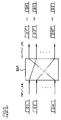
- the switching circuit 641 carries out switch between input and output lines in such a manner as illustrated in Fig. 5. Specifically, the switching circuit 641 converts data D1, D2 and Dm received therein through input lines, into data D1', D2' and Dm' to be output through output lines. As illustrated in Fig. 5, data D1', D2' and Dm' correspond to data Dm, D1 and D2, respectively.
- the thus converted m number of serial data is line-exchanged in the switching circuit 641 in accordance with the exchange information XC transmitted from the exchange information transfer circuit 642 and indicating where the serial data is transferred to.
- the switching circuit 641 carries out switching in such a manner as illustrated in Fig. 5. Specifically, the switching circuit 641 converts data SDAT1, SDAT2 and SDATm received therein, into data SDAT1', SDAT2' and SDATm'. As illustrated in Fig. 5, data SDAT1', SDAT2' and SDATm' correspond to data SDATm, SDAT1 and SDAT2, respectively.
- the serial data SDAT1' to SDATm' is transmitted to the public lines from the switching circuit 641.
- the first conventional data exchange system needs the bus arbitrating circuit 634 as a dedicated circuit, which causes a problem that the data exchange system cannot avoid becoming larger in size.
- the second conventional data exchange system illustrated in Fig. 6 independently uses the data buffer 2-1 to 2-n for each of the CPUs 1-1 to 1-n. Hence, time loss is not generated for data transfer in the data exchange system.
- the data buffer might be increased in size in dependence on capability per CPU for processing subscribers' data, which is accompanied with a problem that the second conventional data exchange system illustrated in Fig. 6 is also increased in size.
- the second conventional data exchange system includes the switching circuit 641 for line-exchange similarly to the first conventional data exchange system, the second conventional data exchange system would become larger in size as the number of lines is increased.
- Japanese Unexamined Patent Publications Nos. 4-252345 and 6-54022 have suggested apparatuses and methods for transferring data through a dual port RAM.
- the above-mentioned problems in the first and second conventional data exchange systems cannot be solved by those apparatuses and methods.
- each one of the memories comprises a dual port random access memory (RAM) having first and second ports, data transmitted from the control circuits being written into the memories through the first port, and the thus written-into data being read out by the reader or reading circuit through the second port.
- the first port may be designed as a serial port, and the second port as a parallel port.
- CPU central processing unit
- the designator or timing pulse generating circuit is designed to transmit selection signals to the memories to thereby monitor access from the control circuits to the memories.
- the designator or timing pulse generating circuit may be designed to monitor at a certain interval which one of the first and second storage areas of the memories each of the control circuits makes access to, and transmits selection signals based on monitoring results so that the reader or reading circuit can read out the data written in one of the first and second storage areas.
- the designator or timing pulse generating circuit includes (a) address decoders in the same number of the control circuits, each of the address decoders decoding an address an associated control circuit made access to, (b) access point latches in association with the address decoders, each of the access point latches storing therein a result of decoding made by an associated address decoder, and (c) a selection signal generating circuit for transmitting selection signals to the memories, based on the result stored in each one of the access point latches.
- the data exchange system may further include an inverter for inverting a signal, and wherein a first bit latch is activated when receiving a signal, and a second bit latch is activated when receiving an inverted signal inverted by the inverter.
- a method of data exchange including the steps of (a) designating each one of control circuits an area into which data is to be written, (b) storing data transmitted from one of the control circuits, in the thus designated area in one of memories, and (c) reading out the data stored in the designated area in the one of memories.
- the method may further include the step of converting parallel data transmitted from the memories to serial data, in which case it is preferable that the parallel data is transmitted from all of the memories through a common bus.
- step (a) further includes (a-1) decoding an address each one of the control circuit made access to, (a-2) storing therein a result of decoding carried out in the step (a-1), and (a-3) transmitting selection signals to the memories, based on the result of decoding.
- Fig. 4 is a time chart illustrating an operation of the first conventional data exchange system illustrated in Fig. 3.
- Fig. 11 is a block diagram of an access point latch of a timing generating circuit illustrated in Fig. 10.
- Fig. 12 is a time chart illustrating an operation of the data exchange system illustrated in Fig. 10.
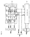
- the illustrated data exchange system includes the n number of CPUs 1-1 to 1-n, dual port RAMs 2-1 to 2-n in the same number as the number of CPUs so that the dual port RAMs 2-1 to 2-n are associated with the CPUs one to one, an exchange information transfer circuit 3 for transmitting exchange information XC1 to XCn to each one of the CPUs 1-1 to 1-n, a timing pulse generating circuit 4 which receives address buses ADD1 to ADDn from the CPUs 1-1 to 1-n, and transmits selection signals SEL1 to SELn to the dual port RAMs 2-1 to 2-n to thereby designate an area into which data is to be written, and a parallel/serial (P/S) converting circuit 5.
- P/S parallel/serial
- Each of the dual port RAMs 2-1 to 2-n stores data transmitted from an associated CPU 1-1 to 1-n through an associated data bus DBUS1 to DBUSn.
- the P/S converting circuit 5 receives parallel data PDT from all of the dual port RAMs 2-1 to 2-n, and converts the received parallel data PDT into serial data SDAT1' to SDATm'.
- the data exchange system in accordance with the embodiment is different from the conventional data exchange system in that the line exchange circuit 64 (see Fig. 3) is eliminated, that the exchange information XC1 to XCn is transmitted to each of the CPUs 1-1 to 1-n, that each one of the dual port RAMs 2-1 to 2-n is in association with each one of CPUs 1-1 to 1-n, and that the timing generating circuit 4 transmits the selection signals SEL1 to SELn to each one of the dual port RAMs 2-1 to 2-n to thereby control the dual port RAMs 2-1 to 2-n in operation.
- the data exchange system has the following structure in order to avoid the system from being increased in size.
- the above-mentioned structure makes it possible to eliminate a line exchange circuit which is a major factor for increasing a data exchange system in size.
- the number of communication signals or the number of addresses between the dual port RAMs and the P/S converting circuit is reduced by using a common bus connecting them with each other.
- each of dual port RAMs 2-1 to 2-n is designed to have an internal area divided into two sections A and B.
- Each of the sections A and B is further divided into the m number of areas, corresponding to the m number of lines, in order to store subscribers' data D1 to Dm in each one of the divided areas.
- the sections A and B are alternately used.
- the exchange information transfer circuit 3 is designed to in advance receive the exchange information XC1 to XCn in the form of matrix table from an upstream system (not illustrated), and transmit the exchange information XC1 to XCn to each one of the CPUs 1-1 to 1-n.
- Each one of the CPUs 1-1 to 1-n stores the processed data into an area designated by the exchange information XC1 to XCn among the m number of the areas in each of the sections A and B in each one of dual port RAMs 2-1 to 2-n.
- the timing generating circuit 4 monitors at a certain interval addresses to which each one of the CPUs 1-1 to 1-n made access, and stores at the interval which CPU made access to which area in an associated dual port RAM. Then, the timing generating circuit 4 transmits the selection signal SEL1 to SELn to one of the dual port RAMs 2-1 to 2-n at a next internal in accordance with the monitoring result.
- the P/S converting circuit 5 transmits an address PAD to one of the dual port RAMs 2-1 to 2-n in synchronization with the timing signals TIM transmitted from the timing generating circuit 4, and reads the parallel data out of the dual port RAM to which the address PAD was transmitted. Then, the P/S converting circuit 5 converts the thus read-out parallel data into serial data, and successively outputs the thus converted serial data.
- the thus processed data is transmitted to and stored in the designated area among the m number of areas in an associated dual port RAM 2-1 to 2-n through both an associated data bus DBUS1 to DBUSn and an associated address bus ADD1 to ADDn in accordance with the exchange information XC1 to XCn having been in advance transmitted from the exchange information transfer circuit 3.
- the timing generating circuit 4 monitors at a certain interval which area each one of the CPUs 1-1 to 1-n made access to, and transmits the selection signal SEL1 to SELn to each one of the dual port RAMs 2-1 to 2-n.
- the P/S converting circuit 5 selects the area among the m number of areas, from which data is to be read out, based on the received selection signal SEL1 to SELn. Then, the P/S converting circuit 5 transmits the address PAD to one of the dual port RAMs 2-1 to 2-n to which the selection signal SEL1 to SELn has been transmitted, in synchronization with the timing signal TIM transmitted from the timing generating circuit 4, to thereby read out the parallel data PDT from the selected dual port RAM.
- the thus read-out m number of parallel data PDT is converted into the m number of serial data in the P/S converting circuit 5, and then output as the line-exchanged serial data SDAT1' to SDATm'.
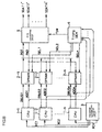
- each one of the dual port RAMs 2-1 and 2-2 is designed to have the storage sections A and B each of which is divided into the m number of storage areas. In Fig. 10, only one of the storage sections A and B is illustrated. Now suppose that data is to be written into the storage areas Nos. 1, 4, 7 and 8 (hatched areas) in the dual port RAM 2-1, and data is to be written into the storage areas Nos. 2, 3, 5 and 6 (hatched areas) in the dual port RAM 2-2.
- the timing generating circuit 4 includes an address decoder 41-1 for decoding an address to which CPU 1-1 made access, an access point latch for 42-1 for storing therein a result of decoding made by the address decoder 41-1, an address decoder 41-2 for decoding an address to which CPU 1-2 made access to, an access point latch for 42-2 for storing therein a result of decoding made by the address decoder 41-2, and a dual port RAM selection signal generating circuit 40 for transmitting a selection signal SEL1 to the dual port RAM 2-1 or a selection signal SEL2 to the dual port RAM 2-2 in dependence on what is stored in the access point latches 42-1 and 42-2.
- the P/S converting circuit 5 is designed to include a P/S conversion circuit 51 for converting parallel data read out of each one of the dual port RAMs 2-1 and 2-2, into serial data, and a dual port RAM address counter 52 for transmitting a data load pulse 521 and a P/S load pulse 522 to the P/S conversion circuit 51, and for transmitting the parallel address PAD to one of the dual port RAMs 2-1 and 2-2.
- the exchange information transfer circuit 3 receives exchange information from an upstream system (not illustrated), and transmits the thus received exchange information to CPU 1-1 and CPU 1-2.
- the data processed by CPU 1-1 is written into an area indicated by the exchange information among the areas Nos. 1, 4, 7 and 8 in the dual port RAM 2-1.
- the data processed by CPU 1-2 is written into an area indicated by the exchange information among the areas Nos. 2, 3, 5 and 6 in the dual port RAM 2-2.
- the access point latch 42-1 includes the m number of flip-flops 421-1 to 421-m each of which has a clock input terminal at which one of decode outputs dec 1 to dec m transmitted from the address decoder 41-1 is received, D input terminal fixed at a high level, and Q output terminal for transmitting an output in accordance with the decode output received at the clock input terminal, two m-bit latches 422-A and 422-B for latching the outputs transmitted from the flip-flops 421-1 to 421-m, the m number of selectors 423-1 to 423-m receiving outputs transmitted from the m-bit latches 422-A and 422-B, and a m-bit selector 424 for latching outputs transmitted from the selectors 423-1 to 423-m.
- the m-bit latches 422-A and 422-B corresponds
- a bit ADDmax which is an uppermost grade bit in an address to the dual port RAMs is input into the m-bit latch 422-A and 422B as a clock for switching the storage section A to the storage section B, and vice versa.
- a bit ADDmax which is an uppermost grade bit in the parallel address PAD transmitted from the dual port RAM address counter 52 is inverted by an inverter 43, and the thus inverted bit ADDmax is input into the m-bit latch 422-B associated with the section B. In this way, the m-bit latch 422-A or 422-B is alternately used in accordance with a sign of the uppermost grade bit ADDmax. Addresses ADD except the uppermost grade bit ADDmax are input into the m-bit selector 424 as selection signals.
- the access point latch 42-2 has the same structure as that of the access point latch 42-1 except that the access point latch 42-2 receives decode results transmitted from the address decoder 41-2.
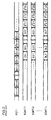
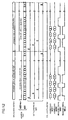
- Fig. 12 illustrates an uppermost grade bit ADDmax in an address, addresses ADD except the uppermost grade bit ADDmax, the data load pulse 521 and the P/S load pulse 522 both transmitted from the dual port RAM address counter 52, addresses on each of the address buses ADD1 and ADD 2, and the selection signals SEL 1 and SEL 2 both transmitted from the timing generating circuit 4.
- the selection signals SEL 1 and SEL 2 indicate selected condition when in a high level, and non-selected condition when in a low level.
- the parallel address PAD transmitted from the dual port RAM address counter 52 is input into the dual port RAMs 2-1 and 2-2, and data is read out of the storage section A of the dual port RAMs 2-1 and 2-2 through the parallel ports in accordance with the sign of the uppermost grade bit ADDmax in the address.
- the address ADD except the uppermost grade bit ADDmax is successively varied from 1 to m one by one.
- the thus varied address ADD together with the data load pulse 521 is input into the P/S converting circuit 51.
- the P/S load pulse 522 is further input into the P/S converting circuit 51 at a timing at which the storage section to which CPUs 1-1 and 1-2 make access is switched.
- the selection signals SEL 1 and SEL 2 transmitted to the dual port RAMs 2-1 and 2-2 are varied in such a manner as illustrated in Fig. 12, and thus, only the hatched areas Nos. 1, 4, 7 and 8 (see Fig. 10) in the dual port RAM 2-1 or Nos. 2, 3, 5 and 6 in the dual port RAM 2-2 are selected.
- the parallel data is input into the P/S converting circuit 5 from the dual port RAMs 2-1 and 2-2, and then, is converted into serial data, which is then output.
- the data exchange system in accordance with the embodiment eliminates a line exchange circuit and a bus arbitrating circuit both of which were absolutely necessary for operation in conventional data exchange systems.
- the data exchange system is designed to have memories in association with each one of the control circuits or CPUs, and carries out line-exchange by designating an area into which data is to be written, in accordance with exchange information, and writing data into the thus designated area. This makes it possible to prevent the data exchange system from being increased in size, even if the line number was increased.
- each one of the dual port RAMs as memories is designed to have two storage sections for storing data therein.
- the two storage sections are alternately used for writing data thereinto or reading out data thereof. This enhances an efficiency in line exchange.
Landscapes
- Engineering & Computer Science (AREA)
- Computer Networks & Wireless Communication (AREA)
- Signal Processing (AREA)
- Exchange Systems With Centralized Control (AREA)
- Mobile Radio Communication Systems (AREA)
- Data Exchanges In Wide-Area Networks (AREA)
Applications Claiming Priority (3)
| Application Number | Priority Date | Filing Date | Title |
|---|---|---|---|
| JP7486097A JP3196107B2 (ja) | 1997-03-27 | 1997-03-27 | データ交換システム |
| JP7486097 | 1997-03-27 | ||
| JP74860/97 | 1997-03-27 |
Publications (2)
| Publication Number | Publication Date |
|---|---|
| EP0868046A2 true EP0868046A2 (fr) | 1998-09-30 |
| EP0868046A3 EP0868046A3 (fr) | 2003-11-19 |
Family
ID=13559510
Family Applications (1)
| Application Number | Title | Priority Date | Filing Date |
|---|---|---|---|
| EP19980105445 Withdrawn EP0868046A3 (fr) | 1997-03-27 | 1998-03-25 | Procédé et système pour échange de données |
Country Status (3)
| Country | Link |
|---|---|
| US (1) | US6751201B1 (fr) |
| EP (1) | EP0868046A3 (fr) |
| JP (1) | JP3196107B2 (fr) |
Families Citing this family (3)
| Publication number | Priority date | Publication date | Assignee | Title |
|---|---|---|---|---|
| US6507732B1 (en) * | 1999-09-14 | 2003-01-14 | Lucent Technologies Inc. | Dynamic path gain compensation for radios in wireless communication systems |
| KR20030053891A (ko) * | 2001-12-24 | 2003-07-02 | 엘지전자 주식회사 | 듀얼포트램을 이용한 데이터 타이밍 및 포맷 변환 장치 |
| JP4396657B2 (ja) * | 2006-03-16 | 2010-01-13 | ソニー株式会社 | 通信装置及び送信制御方法及び送信制御プログラム |
Family Cites Families (17)
| Publication number | Priority date | Publication date | Assignee | Title |
|---|---|---|---|---|
| US4096568A (en) * | 1976-09-24 | 1978-06-20 | Sperry Rand Corporation | Virtual address translator |
| JPS5350908A (en) * | 1976-10-20 | 1978-05-09 | Sanyo Electric Co Ltd | Broadcast receiving memory unit |
| US4156906A (en) * | 1977-11-22 | 1979-05-29 | Honeywell Information Systems Inc. | Buffer store including control apparatus which facilitates the concurrent processing of a plurality of commands |
| FR2503513A1 (fr) * | 1981-04-03 | 1982-10-08 | Cit Alcatel | Autocommutateur temporel a commande repartie |
| US4520477A (en) * | 1983-06-27 | 1985-05-28 | At&T Bell Laboratories | Control information communication arrangement for a time division switching system |
| JPS61115183A (ja) * | 1984-11-09 | 1986-06-02 | Toshiba Corp | 濃淡画像処理における濃度階調変換方式 |
| FR2645987B1 (fr) * | 1989-04-13 | 1991-06-07 | Bull Sa | Dispositif d'acceleration des acces memoire dans un systeme informatique |
| US4991168A (en) * | 1989-05-08 | 1991-02-05 | At&T Bell Laboratories | Concurrent multi-stage network control arrangement |
| ATE114922T1 (de) * | 1989-08-31 | 1994-12-15 | Siemens Ag | Verfahren zur vermittlung von jeweils auf mehrere zeitfächer von zeitkanälen verteilt übertragenen sprach- und/oder daten-informationen. |
| US5309432A (en) * | 1992-05-06 | 1994-05-03 | At&T Bell Laboratories | High-speed packet switch |
| JPH0767154A (ja) * | 1993-08-25 | 1995-03-10 | Fujitsu Ltd | タイムスイッチのアドレス変換装置 |
| FR2718262B1 (fr) * | 1994-03-31 | 1996-05-24 | Sgs Thomson Microelectronics | Mémoire tampon à adressage modulo. |
| US5530924A (en) * | 1994-07-05 | 1996-06-25 | Ford Motor Company | Radio station memory presets with stored audio effects |
| US5592480A (en) * | 1995-03-13 | 1997-01-07 | Carney; Ronald R. | Wideband wireless basestation making use of time division multiple-access bus having selectable number of time slots and frame synchronization to support different modulation standards |
| US5519701A (en) * | 1995-03-29 | 1996-05-21 | International Business Machines Corporation | Architecture for high performance management of multiple circular FIFO storage means |
| US5943242A (en) * | 1995-11-17 | 1999-08-24 | Pact Gmbh | Dynamically reconfigurable data processing system |
| US5802052A (en) * | 1996-06-26 | 1998-09-01 | Level One Communication, Inc. | Scalable high performance switch element for a shared memory packet or ATM cell switch fabric |
-
1997
- 1997-03-27 JP JP7486097A patent/JP3196107B2/ja not_active Expired - Fee Related
-
1998
- 1998-03-25 EP EP19980105445 patent/EP0868046A3/fr not_active Withdrawn
- 1998-03-27 US US09/049,964 patent/US6751201B1/en not_active Expired - Fee Related
Also Published As
| Publication number | Publication date |
|---|---|
| JPH10271551A (ja) | 1998-10-09 |
| US6751201B1 (en) | 2004-06-15 |
| JP3196107B2 (ja) | 2001-08-06 |
| EP0868046A3 (fr) | 2003-11-19 |
Similar Documents
| Publication | Publication Date | Title |
|---|---|---|
| US5363484A (en) | Multiple computer system with combiner/memory interconnection system employing separate direct access link for transferring information packets | |
| US20010005873A1 (en) | Shared memory multiprocessor performing cache coherence control and node controller therefor | |
| JPH02263260A (ja) | メモリアクセススイッチネットワーク | |
| KR910003382B1 (ko) | 레지스터를 구비한 반도체 메모리 장치 | |
| US6434035B2 (en) | Memory system | |
| US3804987A (en) | Multiplexing apparatus having interlaced and/or parallel data transfer with a data processor and communication lines | |
| US6751201B1 (en) | Data exchange system and method of data exchange | |
| KR0147503B1 (ko) | Tec 연동시험이 가능한 타임스위치장치 | |
| AU749380B2 (en) | Time division multiplex highway switch control system and control method of T-S-T three-stage switches in electronic switching system | |
| US5379395A (en) | Semiconductor integrated circuit for central processor interfacing which enables random and serial access to single port memories | |
| US6895478B2 (en) | Memory control circuit | |
| US4569040A (en) | Electronic switching system having a time division multiplex switch controller address by central control unit | |
| US4630197A (en) | Anti-mutilation circuit for protecting dynamic memory | |
| US6529509B1 (en) | Switch controlling apparatus for small capacitance ATM exchange | |
| AU749570B2 (en) | Remote module control system for controlling module disposed at remote place which accommodates line/trunk circuit and control method thereof | |
| JP2697460B2 (ja) | クロック乗換回路 | |
| JP2984594B2 (ja) | マルチクラスタ情報処理システム | |
| KR0153016B1 (ko) | 전전자 교환기용 시공간 분할 스위칭 회로 | |
| KR100288752B1 (ko) | 가입자 보드와 가입자 제어 인터페이스 보드간의 정합장치 | |
| JPS59226962A (ja) | デ−タ交換装置 | |
| JPH10173618A (ja) | バススイッチ装置およびその転送順序変換方法 | |
| JPS63258137A (ja) | タイムスロツトデ−タの変換方法 | |
| JPS644385B2 (fr) | ||
| JPH10312355A (ja) | 制御ユニット及び通信システム | |
| JP2002149485A (ja) | 半導体記憶制御装置 |
Legal Events
| Date | Code | Title | Description |
|---|---|---|---|
| PUAI | Public reference made under article 153(3) epc to a published international application that has entered the european phase |
Free format text: ORIGINAL CODE: 0009012 |
|
| AK | Designated contracting states |
Kind code of ref document: A2 Designated state(s): AT BE CH DE DK ES FI FR GB GR IE IT LI LU MC NL PT SE |
|
| AX | Request for extension of the european patent |
Free format text: AL;LT;LV;MK;RO;SI |
|
| PUAL | Search report despatched |
Free format text: ORIGINAL CODE: 0009013 |
|
| AK | Designated contracting states |
Kind code of ref document: A3 Designated state(s): AT BE CH DE DK ES FI FR GB GR IE IT LI LU MC NL PT SE |
|
| AX | Request for extension of the european patent |
Extension state: AL LT LV MK RO SI |
|
| 17P | Request for examination filed |
Effective date: 20031105 |
|
| 17Q | First examination report despatched |
Effective date: 20031219 |
|
| STAA | Information on the status of an ep patent application or granted ep patent |
Free format text: STATUS: THE APPLICATION HAS BEEN WITHDRAWN |
|
| 18W | Application withdrawn |
Effective date: 20040513 |