EP0868742B1 - Verfahren zur herstellung eines mos-transistors - Google Patents
Verfahren zur herstellung eines mos-transistors Download PDFInfo
- Publication number
- EP0868742B1 EP0868742B1 EP96945893A EP96945893A EP0868742B1 EP 0868742 B1 EP0868742 B1 EP 0868742B1 EP 96945893 A EP96945893 A EP 96945893A EP 96945893 A EP96945893 A EP 96945893A EP 0868742 B1 EP0868742 B1 EP 0868742B1
- Authority
- EP
- European Patent Office
- Prior art keywords
- electrode
- layer
- webs
- mask
- auxiliary
- Prior art date
- Legal status (The legal status is an assumption and is not a legal conclusion. Google has not performed a legal analysis and makes no representation as to the accuracy of the status listed.)
- Expired - Lifetime
Links
Images



Classifications
-
- H—ELECTRICITY
- H10—SEMICONDUCTOR DEVICES; ELECTRIC SOLID-STATE DEVICES NOT OTHERWISE PROVIDED FOR
- H10D—INORGANIC ELECTRIC SEMICONDUCTOR DEVICES
- H10D30/00—Field-effect transistors [FET]
- H10D30/01—Manufacture or treatment
- H10D30/021—Manufacture or treatment of FETs having insulated gates [IGFET]
- H10D30/0223—Manufacture or treatment of FETs having insulated gates [IGFET] having source and drain regions or source and drain extensions self-aligned to sides of the gate
- H10D30/0227—Manufacture or treatment of FETs having insulated gates [IGFET] having source and drain regions or source and drain extensions self-aligned to sides of the gate having both lightly-doped source and drain extensions and source and drain regions self-aligned to the sides of the gate, e.g. lightly-doped drain [LDD] MOSFET or double-diffused drain [DDD] MOSFET
-
- H—ELECTRICITY
- H10—SEMICONDUCTOR DEVICES; ELECTRIC SOLID-STATE DEVICES NOT OTHERWISE PROVIDED FOR
- H10P—GENERIC PROCESSES OR APPARATUS FOR THE MANUFACTURE OR TREATMENT OF DEVICES COVERED BY CLASS H10
- H10P10/00—Bonding of wafers, substrates or parts of devices
-
- H—ELECTRICITY
- H10—SEMICONDUCTOR DEVICES; ELECTRIC SOLID-STATE DEVICES NOT OTHERWISE PROVIDED FOR
- H10D—INORGANIC ELECTRIC SEMICONDUCTOR DEVICES
- H10D30/00—Field-effect transistors [FET]
- H10D30/60—Insulated-gate field-effect transistors [IGFET]
- H10D30/67—Thin-film transistors [TFT]
- H10D30/6729—Thin-film transistors [TFT] characterised by the electrodes
- H10D30/673—Thin-film transistors [TFT] characterised by the electrodes characterised by the shapes, relative sizes or dispositions of the gate electrodes
-
- H—ELECTRICITY
- H10—SEMICONDUCTOR DEVICES; ELECTRIC SOLID-STATE DEVICES NOT OTHERWISE PROVIDED FOR
- H10D—INORGANIC ELECTRIC SEMICONDUCTOR DEVICES
- H10D64/00—Electrodes of devices having potential barriers
- H10D64/01—Manufacture or treatment
- H10D64/013—Manufacture or treatment of electrodes having a conductor capacitively coupled to a semiconductor by an insulator
- H10D64/01302—Manufacture or treatment of electrodes having a conductor capacitively coupled to a semiconductor by an insulator the insulator being formed after the semiconductor body, the semiconductor being silicon
- H10D64/01304—Manufacture or treatment of electrodes having a conductor capacitively coupled to a semiconductor by an insulator the insulator being formed after the semiconductor body, the semiconductor being silicon characterised by the conductor
- H10D64/01324—Manufacture or treatment of electrodes having a conductor capacitively coupled to a semiconductor by an insulator the insulator being formed after the semiconductor body, the semiconductor being silicon characterised by the conductor characterised by the sectional shape, e.g. T or inverted-T
-
- H—ELECTRICITY
- H10—SEMICONDUCTOR DEVICES; ELECTRIC SOLID-STATE DEVICES NOT OTHERWISE PROVIDED FOR
- H10D—INORGANIC ELECTRIC SEMICONDUCTOR DEVICES
- H10D64/00—Electrodes of devices having potential barriers
- H10D64/01—Manufacture or treatment
- H10D64/013—Manufacture or treatment of electrodes having a conductor capacitively coupled to a semiconductor by an insulator
- H10D64/01302—Manufacture or treatment of electrodes having a conductor capacitively coupled to a semiconductor by an insulator the insulator being formed after the semiconductor body, the semiconductor being silicon
- H10D64/01304—Manufacture or treatment of electrodes having a conductor capacitively coupled to a semiconductor by an insulator the insulator being formed after the semiconductor body, the semiconductor being silicon characterised by the conductor
- H10D64/01326—Aspects related to lithography, isolation or planarisation of the conductor
- H10D64/01328—Aspects related to lithography, isolation or planarisation of the conductor by defining the conductor using a sidewall spacer mask, a transformation under a mask or a plating at a sidewall
-
- H—ELECTRICITY
- H10—SEMICONDUCTOR DEVICES; ELECTRIC SOLID-STATE DEVICES NOT OTHERWISE PROVIDED FOR
- H10D—INORGANIC ELECTRIC SEMICONDUCTOR DEVICES
- H10D64/00—Electrodes of devices having potential barriers
- H10D64/20—Electrodes characterised by their shapes, relative sizes or dispositions
- H10D64/23—Electrodes carrying the current to be rectified, amplified, oscillated or switched, e.g. sources, drains, anodes or cathodes
- H10D64/251—Source or drain electrodes for field-effect devices
- H10D64/258—Source or drain electrodes for field-effect devices characterised by the relative positions of the source or drain electrodes with respect to the gate electrode
- H10D64/259—Source or drain electrodes being self-aligned with the gate electrode and having bottom surfaces higher than the interface between the channel and the gate dielectric
-
- H—ELECTRICITY
- H10—SEMICONDUCTOR DEVICES; ELECTRIC SOLID-STATE DEVICES NOT OTHERWISE PROVIDED FOR
- H10D—INORGANIC ELECTRIC SEMICONDUCTOR DEVICES
- H10D64/00—Electrodes of devices having potential barriers
- H10D64/20—Electrodes characterised by their shapes, relative sizes or dispositions
- H10D64/27—Electrodes not carrying the current to be rectified, amplified, oscillated or switched, e.g. gates
- H10D64/311—Gate electrodes for field-effect devices
- H10D64/411—Gate electrodes for field-effect devices for FETs
- H10D64/511—Gate electrodes for field-effect devices for FETs for IGFETs
- H10D64/517—Gate electrodes for field-effect devices for FETs for IGFETs characterised by the conducting layers
- H10D64/518—Gate electrodes for field-effect devices for FETs for IGFETs characterised by the conducting layers characterised by their lengths or sectional shapes
Definitions
- the channel area is facing Flanks of connections of the source / drain regions insulating Spacer formed, above which the gate electrode is formed becomes.
- the upper part of the gate electrode overlaps the insulating one Spacer on the side.
- the gate electrode is made of two different metal layers educated. After structuring the top metal layer the lower metal layer is under the side Etched back dimensions of the top metal layer.
- the RC constants are the gate electrodes are no longer negligible.
- the resistance of the usually doped and increases possibly silicided or with other more conductive Materials coated polysilicon existing gate electrode with a smaller edge length, for example due to grain boundary influences is returned.
- the invention is based on the problem of a method for Specify manufacture of a MOS transistor with a short channel length.
- the MOS transistor manufactured according to the invention has one Gate electrode with a T-shaped cross section.
- the gate electrode points at the bottom, on the surface Gate dielectric, smaller feature sizes than in the upper one Area.
- the top of the gate electrode which is the gate dielectric facing away, determines the line resistance the gate electrode.
- the bottom of the gate electrode on the interface to the gate dielectric determines the channel length, that for the switching speed of the MOS transistor is decisive. Because the structure sizes of the gate electrode in the MOS transistor of the invention Surface to the gate dielectric and on the opposite Surface that determines the line resistance of the gate electrode, the channel length is independent set by the contact resistance of the gate electrode.
- the MOS transistor manufactured according to the invention is special Can be used with channel lengths below 100 nm, because in this area the resistance of a polysilicon containing Gate electrode due to the increasing influence of grain boundaries increases more than the reduction in area.
- MOS transistor produced according to the invention is that even with channel lengths below 100 nm, for example, with the gate electrode in the upper area Structure sizes ⁇ 250 nm can be realized. So that can a further reduction in resistance of the gate electrode Application of metal silicide, for example titanium silicide, achieved become. It has been shown that titanium silicide at Structure sizes below 250 nm increasingly a phase of high resistance and with such small structures for resistance reduction is not well suited.
- the gate electrode of the MOS transistor is preferably turned off two electrode layers in two independent structuring steps manufactured.
- the first electrode layer can also be formed by a other fine structuring technology, for example with the help of Electron beam lithography, are structured.
- a planarizing layer is formed so that the structured first electrode layer in the upper Area exposed. Outside the structured first electrode layer is the surface of the gate dielectric of the planarizing layer.
- one second electrode layer deposited and structured. The Structure sizes are larger than in the first structured one Electrode layer.
- the structuring of the second electrode layer can both using a photoresist mask as well as self-adjusting respectively.
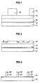
- a gate dielectric 12 is applied to a substrate 11, which comprises silicon at least in the area of a main surface, for example a monocrystalline silicon structure or an SOI substrate (see FIG. 1).
- the gate dielectric 12 is formed, for example, by thermal oxidation from SiO 2 in a layer thickness of 3 to 4 nm.
- a first electrode layer is applied to the gate dielectric 12 13 applied.
- the first electrode layer 13 becomes, for example made of doped polysilicon in a layer thickness of for example generated 200 nm.
- An auxiliary layer 14 is formed on the first electrode layer 13, for example by deposition in a TEOS process from SiO 2 .
- the auxiliary layer 14 has a thickness of, for example, 200 nm.
- a photoresist mask 15 is formed on the auxiliary layer 14.
- An auxiliary structure 14 ' is formed from the auxiliary layer 14 by anisotropic etching, for example using CHF 3 -RIE (reactive ion etching).
- the auxiliary structure 14 ' has essentially vertical flanks.
- the auxiliary structure 14 ' completely covers the surface of the first electrode layer 13 (see FIG. 2).
- the auxiliary structure 14 ' preferably has elevations arranged regularly.
- Edge coverage and anisotropic etching with, for example HBr-RIE (Reactive Ion Etching) are on the flanks of the Auxiliary structure 14 'spacer 16 formed from polysilicon.
- the layer is deposited in a thickness of, for example, 100 nm.
- the width of the spacers 16 is, for example consequently also 100 nm.
- the arrangement of the spacers 16 is predetermined by the arrangement of the flanks of the auxiliary structure 14 '.
- the auxiliary layer 14 ' is structured by anisotropic etching, for example using CHF 3 and CF 4 -RIE (reactive ion etching). This creates a hard mask 14 ′′ (see FIG. 3).
- Anisotropic etching with, for example, HBr is carried out, in which 13 electrode webs from the first electrode layer 13 'are formed.
- the hard mask 14 ′′ is used for this Etching process not attacked and restores the edge Transfer of the structure to the electrode webs 13 'safely.
- the LDD regions can also be doped by diffusion out of doped spacers.
- Thick SiO 2 spacers 17 are then produced on the flanks of the electrode webs 13 'and an HDD implantation is carried out to form source / drain regions 18 (see FIG. 4).
- the HDD (“heavily doped drain”) implantation is carried out, for example, with arsenic at an energy of 90 keV and a dose of 5 x 10 15 cm -2 .
- An SiO 2 layer is deposited over the entire surface, for example BPSG (boron-phosphorus-silicate glass), which covers the electrode webs 13 'and which fills the spaces between adjacent electrode webs 13'.
- the reference number 19 denotes the SiO 2 layer, the thick SiO 2 spacers 17, the thin SiO 2 spacers and the hard mask 14 ′′ (see FIG. 5).
- the SiO 2 layer is deposited in a thickness of, for example, 300 nm.
- the SiO 2 layer 19 is etched back until its thickness is less than the height of the electrode webs 13 '.
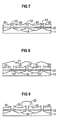
- the electrode webs 13 are then, for example, wet-chemical with choline to the level of the planarizing Layer 20 etched back (see Figure 7). This takes place on Example around 100 nm, around the second electrode layer if possible to be able to deposit planar.
- a second electrode layer 21 is subsequently formed over the entire surface deposited.
- the second electrode layer 21 is, for example made of doped polysilicon in a layer thickness of for example 200 nm deposited (see Figure 8).
- the second Electrode layer 21 is connected to the electrode webs 13 '.
- a mask is created (not shown) that matches the shape a gate electrode 22 defined in the upper region.
- Anisotropic etching with HBr becomes the second electrode layer 21 outside the mask and the electrode bars 13 'removed outside the mask.
- the etching stops on the Surface of the planarizing layer 20 or, in the area the electrode webs 13 ', the gate dielectric 12 the gate electrode 22, which is part of the electrode lands 13 'and a part of the second electrode layer 21 (see Figure 9).
- the structure size of the gate electrode 22 the surface of the gate dielectric 12 is defined by the width the spacer 16 determines. For example, it is 100 nm the structure size becomes the side facing away from the gate dielectric 12 the gate electrode 22 through the structuring the mask used for the second electrode layer 21.
- the structure size in the upper area is, for example 300 nm.
- the planarizing layer 20 is then selectively etched back to the silicon substrate 11 and to the gate electrode 22. This is done, for example, by isotropic etching with NH 4 , HF.
- the MOS transistor is optionally completed by a second HDD implantation with, for example, arsenic at an energy of, for example, 90 keV and a dose of, for example, 5 ⁇ 10 15 cm -2 .
- the source / drain regions and, if appropriate, the gate electrodes can be silicided. These steps are not shown in detail.
- a gate dielectric 22 is applied to a substrate 21 which has silicon at least in the area of a main surface, for example a monocrystalline silicon wafer or an SOI substrate.
- the gate dielectric 22 is formed, for example, by thermal oxidation from SiO 2 in a layer thickness of 3 to 4 nm (see FIG. 10).
- a photoresist mask 25 is produced on the auxiliary layer 24.
- An auxiliary structure 24 ′ is formed from the auxiliary layer 24 by anisotropic etching, for example using CHF 3 -RIE (reactive ion etching).
- the auxiliary structure 24 ' has vertical flanks.
- the auxiliary structure 24 ' completely covers the surface of the first electrode layer 23 (see FIG. 11). It preferably has regularly arranged surveys.
- a hard mask 24 ′′ is formed by structuring the auxiliary layer 24 ′ by anisotropic etching using, for example, CHF 3 , CF 4 -RIE (reactive ion etching).
- the spacers 26 act as an etching mask.
- the first electrode layer 23 is structured by anisotropic etching, for example using HBr, for example. This creates electrode webs 23 ', which are preferably arranged regularly (see FIG. 12). In this etching process, the spacers 26 are removed from polysilicon. Since the etching is selective to SiO 2 , it stops on the surface of the hard mask 24 ′′ and of the gate dielectric 22.
- SiO 2 spacers 27 for an LDD implantation 28 are optionally produced on the flanks of the electrode webs 23 '.
- the implantation is carried out, for example, with arsenic with an energy of, for example, 20 keV and a dose of 5 ⁇ 10 14 cm -2 (see FIG. 13).
- the LDD doping can also be carried out by diffusion out of doped spacers.
- SiO 2 layer is deposited over the entire surface, which fills the spaces between adjacent electrode webs 23 '.
- the reference symbol 29 denotes the SiO 2 layer, the hard mask 24 ′′, the SiO 2 spacer 27 (see FIG. 14).
- the SiO 2 layer has a thickness of, for example, 300 nm.
- a planarizing layer 30 is formed from the SiO 2 layer 29 by means of planarization methods, for example chemical mechanical polishing or planarization etching.
- the regular arrangement of the electrode webs 23 ' is advantageous, but not absolutely necessary, for the planarization.
- the planarizing layer 30 has a smaller thickness than the first electrode layer 23.
- the planarizing layer 30 has a thickness of, for example, 100 nm (see FIG. 15).
- the electrode webs 23 ' have a height of, for example, 400 nm.
- a mask 31 is generated, which forms part of the electrode webs 23 'covers that for a gate electrode to be produced later are provided. Uncovered by mask 31 Electrode webs 23 '' are made by wet chemical etching Choline etched back to the level of the planarizing layer 30 (see Figure 16).
- the second Electrode layer 32 has a thickness of, for example 100 nm formed from doped polysilicon.
- the second electrode layer 32 stands with the electrode webs 23 '' and 23 ' in connection.
- Anisotropic etching for example with HBr, makes the second one Electrode layer 32, similar to a space etching, etched back. At the same time, the electrode webs 23 '' were uncovered from the mask 31 (see FIG. 18). Since the part of the electrode webs 23 ′ covered by the mask 31 not etched back to the level of the planarizing layer 30 structure in this area significantly higher height. Anisotropic etching remains hence a gate electrode 33 in this area.
- the gate electrode 33 is composed of the part of the electrode webs 23 'and the part of the second arranged above it Electrode layer 33.
- the electrode webs 23 ' are aligned above the protrude planarizing layer 30.
- the electrode bars 23 ' project beyond the planarizing layer 30 by at least the thickness of the planarizing layer 30.
- the ratio of the height of the electrode webs 23 'to the thickness of the planarizing layer 30 for example 4: 1.
- the unnecessary electrode webs can be shown in FIG 23 '', which are not covered by the mask 31, completely can be removed by wet chemical means, and the holes thereby formed after removal of the mask 31 by deposition and Back etching of, for example, 70 nm BPSG can be planarized. Then lower electrode webs 23 'are sufficient. Then is in the embodiment for the ratio of height a value of, for example, to the base side of the electrode webs 23 ' 3.5: 1 instead of 5: 1 is sufficient.
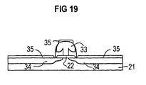
- Anisotropic etching with, for example, CHF 3 removes the exposed part of the planarizing layer 30 and the gate dielectric 22 selectively from silicon.
- the gate electrode 33 acts as a mask.
- an HDD implantation is carried out, for example, with arsenic at an energy of, for example, 90 keV and a dose of, for example, 5 ⁇ 10 15 cm -2 .
- Source / drain regions 34 are formed which also include the LDD regions 28.
- the surfaces of the source / drain regions 34 and the gate electrode 33 are provided with a metal silicide layer 35, for example made of titanium silicide.
- the auxiliary structure 14 'or 24' can also be formed from two partial layers.
- an SiO 2 layer is applied first and then an Si 3 N 4 layer.
- the structuring only the Si 3 N 4 layer is selectively structured to SiO 2 .
Landscapes
- Insulated Gate Type Field-Effect Transistor (AREA)
- Electrodes Of Semiconductors (AREA)
- Metal-Oxide And Bipolar Metal-Oxide Semiconductor Integrated Circuits (AREA)
- Thin Film Transistor (AREA)
Abstract
Description
- Figur 1
- zeigt ein Substrat mit einem Gatedielektrikum, einer ersten Elektrodenschicht, einer Hilfsschicht und einer Photolackmaske.
- Figur 2
- zeigt das Substrat nach Bildung einer Hilfsstruktur und Bildung von Spacern an Flanken der Hilfsstruktur.
- Figur 3
- zeigt das Substrat nach Strukturierung der ersten Elektrodenschicht zu Elektrodenstegen.
- Figur 4
- zeigt das Substrat nach der Bildung von Source/Drain-Gebieten.
- Figur 5
- zeigt das Substrat nach Abscheidung einer SiO2-Schicht, die die Zwischenräume zwischen benachbarten Elektrodenstegen auffüllt.
- Figur 6
- zeigt das Substrat nach Planarisierung der SiO2-Schicht.
- Figur 7
- zeigt das Substrat nach dem Rückätzen der Elektrodenstege.
- Figur 8
- zeigt das Substrat nach Abscheiden einer zweiten Elektrodenschicht.
- Figur 9
- zeigt das Substrat nach der Herstellung einer T-förmigen Gateelektrode.
- Figur 10
- zeigt ein Substrat mit einem Gatedielektrikum, einer ersten Elektrodenschicht, einer Hilfsschicht und einer Photolackmaske.
- Figur 11
- zeigt das Substrat nach Bildung einer Hilfsstruktur und Bildung von Spacern an Flanken der Hilfsstruktur.
- Figur 12
- zeigt das Substrat nach Strukturierung der ersten Elektrodenschicht zu Elektrodenstegen.
- Figur 13
- zeigt das Substrat nach einer LDD-Implantation.
- Figur 14
- zeigt das Substrat nach dem Abscheiden einer SiO2-Schicht, die die Zwischenräume zwischen benachbarten Elektrodenstegen auffüllt.
- Figur 15
- zeigt das Substrat nach Planarisieren der SiO2-Schicht.
- Figur 16
- zeigt das Substrat mit einer Maske, die einen Teil der Elektrodenstege abdeckt, der als Teil einer Gateelektrode vorgesehen ist, und nach dem Rückätzen der von der Maske unbedeckten Elektrodenstege.
- Figur 17
- 7 zeigt das Substrat nach Abscheiden einer zweiten Elektrodenschicht.
- Figur 18
- 3 zeigt das Substrat nach dem Rückätzen der zweiten Elektrodenschicht, wobei die von der Maske unbedeckten Elektrodenstege vollständig entfernt werden und eine Gateelektrode selbstjustiert gebildet wird.
- Figur 19
- zeigt das Substrat nach einer Source/Drain-Implantation und Silizidbildung an der Oberfläche der Source/Drain-Gebiete sowie der Gateelektrode.
Claims (9)
- Verfahren zur Herstellung eines MOS-Transistors,bei dem in einem Substrat, das mindestens im Bereich einer Hauptfläche Silizium umfaßt, ein Sourcegebiet, ein Draingebiet und ein dazwischen angeordnetes Kanalgebiet erzeugt werden,bei dem an der Hauptfläche ein Gatedielektrikum erzeugt wird, das mindestens die Oberfläche des Kanalgebietes bedeckt,bei dem ganzflächig eine erste Elektrodenschicht erzeugt wird,bei dem auf der ersten Elektrodenschicht Hilfsstrukturen mit im wesentlichen senkrecht zur Hauptfläche ausgerichteten Flanken erzeugt werden,bei dem an den Flanken der Hilfsstrukturen Spacer gebildet werden,bei dem die erste Elektrodenschicht entsprechend den Spacern strukturiert wird, wobei Elektrodenstege entstehen,bei dem eine planarisierende Schicht so gebildet wird, daß die Elektrodenstege im oberen Bereich freiliegen, während die Zwischenräume zwischen benachbarten Elektrodenstegen mit der planarisierenden Schicht gefüllt sind,bei dem ganzflächig eine zweite Elektrodenschicht erzeugt wird,bei dem durch Ätzung der zweiten Elektrodenschicht eine Gateelektrode aus einem Teil eines der Elektrodenstege und einem Teil der zweiten Elektrodenschicht gebildet wird.
- Verfahren nach Anspruch 1,bei dem zur Bildung der Hilfsstrukturen auf die erste Elektrodenschicht eine Hilfsschicht aufgebracht wird,bei dem die Hilfsschicht durch anisotropes Ätzen so strukturiert wird, daß die erste Elektrodenschicht mit der Hilfsschicht bedeckt bleibt, und daß in der Hilfsschicht Vertiefungen mit im wesentlichen senkrechten Flanken gebildet werden.
- Verfahren nach Anspruch 2,bei dem die Spacer an den Flanken der Hilfsstrukturen durch Abscheiden und anisotropes Ätzen einer Schicht mit im wesentlichen konformer Kantenbedeckung gebildet werden,bei dem durch anisotropes Ätzen der Hilfsschicht unter Verwendung der Spacer als Ätzmaske eine Hartmaske gebildet wird,bei dem unter Verwendung der Hartmaske als Ätzmaske durch anisotropes Ätzen der ersten Elektrodenschicht die Elektrodenstege gebildet werden.
- Verfahren nach einem der Ansprüche 1 bis 3,bei dem zur Bildung der planarisierenden Schicht eine isolierende Schicht abgeschieden wird, deren Dicke mindestens so groß ist wie der halbe Abstand zwischen benachbarten Elektrodenstegen,bei dem durch ein Planarisierungsverfahren die isolierende Schicht soweit entfernt wird, bis die Elektrodenstege im oberen Bereich freigelegt sind.
- Verfahren nach einem der Ansprüche 1 bis 4, bei dem nach der Bildung der Elektrodenstege eine LDD-Implantation durchgeführt wird.
- Verfahren nach einem der Ansprüche 1 bis 5,bei dem die zweite Elektrodenschicht mit Hilfe einer lithographisch erzeugten Maske strukturiert wird.
- Verfahren nach einem der Ansprüche 1 bis 5,bei dem die planarisierende Schicht so gebildet wird, daß der obere Bereich der Elektrodenstege die planarisierende Schicht um mindestens die Dicke der planarisierenden Schicht überragt,bei dem eine Maske erzeugt wird, die denjenigen Teil der Elektrodenstege abdeckt, der als Teil der Gateelektrode vorgesehen ist,bei dem die von der Maske unbedeckten Teile der Elektrodenstege zurückgeätzt werden,bei dem die Maske entfernt wird,bei dem nach Bildung der zweiten Elektrodenschicht eine anisotrope Ätzung durchgeführt wird, bei der die von der Maske unbedeckten Teile der Elektrodenstege entfernt werden.
- Verfahren nach Anspruch 7,bei dem nach Bildung der Gateelektrode die planarisierende Schicht durch anisotropes Ätzen strukturiert wird, wobei die Gateelektrode als Maske wirkt,bei dem eine Implantation zur Bildung von Sourcegebiet und Draingebiet durchgeführt wird, wobei die Gateelektrode als Maske wirkt,bei dem die Gateelektrode sowie das Sourcegebiet und das Draingebiet mit einer Schicht aus Metallsilizid versehen werden.
- Verfahren nach einem der Ansprüche 1 bis 8, bei dem die erste Elektrodenschicht und die zweite Elektrodenschicht sowie die Spacer aus dotiertem Polysilizium, die Hilfsstrukturen und die planarisierende Schicht aus SiO2 gebildet werden.
Applications Claiming Priority (3)
| Application Number | Priority Date | Filing Date | Title |
|---|---|---|---|
| DE19548058 | 1995-12-21 | ||
| DE19548058A DE19548058C2 (de) | 1995-12-21 | 1995-12-21 | Verfahren zur Herstellung eines MOS-Transistors |
| PCT/DE1996/002235 WO1997023902A2 (de) | 1995-12-21 | 1996-11-21 | Verfahren zur herstellung eines mos-transistors |
Publications (2)
| Publication Number | Publication Date |
|---|---|
| EP0868742A2 EP0868742A2 (de) | 1998-10-07 |
| EP0868742B1 true EP0868742B1 (de) | 2001-08-01 |
Family
ID=7780966
Family Applications (1)
| Application Number | Title | Priority Date | Filing Date |
|---|---|---|---|
| EP96945893A Expired - Lifetime EP0868742B1 (de) | 1995-12-21 | 1996-11-21 | Verfahren zur herstellung eines mos-transistors |
Country Status (7)
| Country | Link |
|---|---|
| US (1) | US6171937B1 (de) |
| EP (1) | EP0868742B1 (de) |
| JP (1) | JP2000502213A (de) |
| KR (1) | KR19990076582A (de) |
| DE (2) | DE19548058C2 (de) |
| TW (1) | TW334603B (de) |
| WO (1) | WO1997023902A2 (de) |
Families Citing this family (13)
| Publication number | Priority date | Publication date | Assignee | Title |
|---|---|---|---|---|
| US6483156B1 (en) * | 2000-03-16 | 2002-11-19 | International Business Machines Corporation | Double planar gated SOI MOSFET structure |
| US7163864B1 (en) * | 2000-10-18 | 2007-01-16 | International Business Machines Corporation | Method of fabricating semiconductor side wall fin |
| DE10056873B4 (de) | 2000-11-16 | 2010-06-17 | Advanced Micro Devices, Inc., Sunnyvale | Verfahren zur Herstellung einer Gateelektrode eines Feldeffekttransistors mit verringertem Gatewiderstand |
| WO2002058158A2 (en) * | 2000-11-16 | 2002-07-25 | Advanced Micro Devices, Inc. | Field effect transistor with redued gate delay and method of fabricating the same |
| DE10101825B4 (de) * | 2001-01-17 | 2006-12-14 | United Monolithic Semiconductors Gmbh | Verfahren zur Herstellung eines Halbleiter-Bauelements mit einer T-förmigen Kontaktelektrode |
| DE10141841C1 (de) * | 2001-08-27 | 2003-03-06 | Infineon Technologies Ag | Verfahren zur Herstellung einer selbstjustierenden Maske |
| DE10141839A1 (de) * | 2001-08-27 | 2002-11-14 | Infineon Technologies Ag | Verfahren zur Herstellung einer selbstjustierenden Maske für eine Struktur mit einer grossen Fläche |
| US6610604B1 (en) | 2002-02-05 | 2003-08-26 | Chartered Semiconductor Manufacturing Ltd. | Method of forming small transistor gates by using self-aligned reverse spacer as a hard mask |
| DE10220999A1 (de) * | 2003-02-06 | 2003-11-20 | United Monolithic Semiconduct | Verfahren zur Herstellung eines Halbleiterbauelements und danach hergestelltes Halbleiterelement |
| DE10304722A1 (de) | 2002-05-11 | 2004-08-19 | United Monolithic Semiconductors Gmbh | Verfahren zur Herstellung eines Halbleiterbauelements |
| US20050130432A1 (en) * | 2003-12-11 | 2005-06-16 | Machala Charles F.Iii | Method for improving transistor leakage current uniformity |
| JP2007306016A (ja) * | 2007-06-19 | 2007-11-22 | Texas Instr Japan Ltd | 半導体装置の製造方法 |
| JP2013172082A (ja) * | 2012-02-22 | 2013-09-02 | Toshiba Corp | パターン形成方法、半導体装置の製造方法および塗布装置 |
Family Cites Families (13)
| Publication number | Priority date | Publication date | Assignee | Title |
|---|---|---|---|---|
| US4358340A (en) * | 1980-07-14 | 1982-11-09 | Texas Instruments Incorporated | Submicron patterning without using submicron lithographic technique |
| US4354896A (en) * | 1980-08-05 | 1982-10-19 | Texas Instruments Incorporated | Formation of submicron substrate element |
| US4432132A (en) * | 1981-12-07 | 1984-02-21 | Bell Telephone Laboratories, Incorporated | Formation of sidewall oxide layers by reactive oxygen ion etching to define submicron features |
| US4689869A (en) * | 1986-04-07 | 1987-09-01 | International Business Machines Corporation | Fabrication of insulated gate gallium arsenide FET with self-aligned source/drain and submicron channel length |
| FR2618011B1 (fr) * | 1987-07-10 | 1992-09-18 | Commissariat Energie Atomique | Procede de fabrication d'une cellule de memoire |
| US5231038A (en) * | 1989-04-04 | 1993-07-27 | Mitsubishi Denki Kabushiki Kaisha | Method of producing field effect transistor |
| DE4032411A1 (de) | 1990-10-12 | 1992-04-16 | Daimler Benz Ag | Verfahren zur herstellung von t-gate-elektroden |
| US5202272A (en) * | 1991-03-25 | 1993-04-13 | International Business Machines Corporation | Field effect transistor formed with deep-submicron gate |
| DE4234777A1 (de) * | 1992-10-15 | 1994-04-21 | Daimler Benz Ag | Verfahren zur naßchemischen Strukturierung von Gate-Elektroden |
| KR960006004A (ko) | 1994-07-25 | 1996-02-23 | 김주용 | 반도체 소자 및 그 제조방법 |
| US5599738A (en) * | 1995-12-11 | 1997-02-04 | Motorola | Methods of fabrication of submicron features in semiconductor devices |
| DE19548056C1 (de) * | 1995-12-21 | 1997-03-06 | Siemens Ag | Verfahren zur Herstellung einer Gateelektrode für eine MOS-Struktur |
| US5893735A (en) * | 1996-02-22 | 1999-04-13 | Siemens Aktiengesellschaft | Three-dimensional device layout with sub-groundrule features |
-
1995
- 1995-12-21 DE DE19548058A patent/DE19548058C2/de not_active Expired - Fee Related
-
1996
- 1996-11-21 US US09/091,150 patent/US6171937B1/en not_active Expired - Fee Related
- 1996-11-21 WO PCT/DE1996/002235 patent/WO1997023902A2/de not_active Ceased
- 1996-11-21 KR KR1019980704653A patent/KR19990076582A/ko not_active Abandoned
- 1996-11-21 EP EP96945893A patent/EP0868742B1/de not_active Expired - Lifetime
- 1996-11-21 JP JP09523199A patent/JP2000502213A/ja not_active Ceased
- 1996-11-21 DE DE59607432T patent/DE59607432D1/de not_active Expired - Fee Related
- 1996-12-19 TW TW085115697A patent/TW334603B/zh active
Also Published As
| Publication number | Publication date |
|---|---|
| DE19548058C2 (de) | 1997-11-20 |
| DE59607432D1 (de) | 2001-09-06 |
| EP0868742A2 (de) | 1998-10-07 |
| JP2000502213A (ja) | 2000-02-22 |
| WO1997023902A2 (de) | 1997-07-03 |
| DE19548058A1 (de) | 1997-06-26 |
| WO1997023902A3 (de) | 1997-09-12 |
| KR19990076582A (ko) | 1999-10-15 |
| TW334603B (en) | 1998-06-21 |
| US6171937B1 (en) | 2001-01-09 |
Similar Documents
| Publication | Publication Date | Title |
|---|---|---|
| EP0968527B1 (de) | Verfahren zur herstellung eines vertikalen mos-transistors | |
| DE3881986T2 (de) | Nichtflüchtige Halbleiterspeicheranordnung und Verfahren zu ihrer Herstellung. | |
| DE102004060171A1 (de) | Charge-trapping-Speicherzelle und Herstellungsverfahren | |
| DE19548056C1 (de) | Verfahren zur Herstellung einer Gateelektrode für eine MOS-Struktur | |
| EP0868742B1 (de) | Verfahren zur herstellung eines mos-transistors | |
| DE4220497A1 (de) | Halbleiterspeicherbauelement und verfahren zu dessen herstellung | |
| DE69627975T2 (de) | MOS-Transistor und Verfahren zu seiner Herstellung | |
| EP1138085B1 (de) | Feldeffektgesteuerter transistor und verfahren zu dessen herstellung | |
| DE4232817B4 (de) | Halbleiter-Speicherzelle und Verfahren zu deren Herstellung | |
| WO2000055904A1 (de) | Dram-zellenanordnung und verfahren zu deren herstellung | |
| DE10109564A1 (de) | Grabenkondensator und Verfahren zu seiner Herstellung | |
| EP1125328B1 (de) | Verfahren zur herstellung einer dram-zellenanordnung | |
| DE102005002739B4 (de) | Verfahren zum Herstellen eines Feldeffekttransistors, Tunnel-Feldeffekttransistor und integrierte Schaltungsanordnung mit mindestens einem Feldeffekttransistor | |
| EP1129482A1 (de) | Verfahren zur Herstellung von einer DRAM-Zellenanordnung | |
| DE19720193A1 (de) | Integrierte Schaltungsanordnung mit mindestens zwei vertikalen MOS-Transistoren und Verfahren zu deren Herstellung | |
| DE10334547B4 (de) | Herstellungsverfahren für einen Grabenkondensator mit einem Isolationskragen, der über einen vergrabenen Kontakt einseitig mit einem Substrat elektrisch verbunden ist | |
| WO2005038930A2 (de) | Verfahren zum strukturieren und feldeffekttransistoren | |
| DE19739755A1 (de) | Halbleitereinrichtung und zugehöriges Herstellungsverfahren | |
| DE10215365A1 (de) | Transistorstruktur unter Verwendung von Epitaxialschichten und Verfahren zur Herstellung derselben | |
| EP0899783B1 (de) | Schaltungsanordnung mit mindestens vier Transistoren und Verfahren zu dessen Herstellung | |
| DE19653107C2 (de) | Verfahren zur Herstellung einer Speicherzellenanordnung | |
| DE102005053509A1 (de) | Verfahren zur Herstellung eines Halbleiterprodukts und Halbleiterprodukt | |
| DD280851A1 (de) | Verfahren zur herstellung von graben-speicherzellen | |
| DE10056873A1 (de) | Feldeffekttransistor mit verringerter Gateverzögerung und Verfahren zur Herstellung desselben | |
| EP1068645B1 (de) | Speicherzellenanordnung und verfahren zu ihrer herstellung |
Legal Events
| Date | Code | Title | Description |
|---|---|---|---|
| PUAI | Public reference made under article 153(3) epc to a published international application that has entered the european phase |
Free format text: ORIGINAL CODE: 0009012 |
|
| 17P | Request for examination filed |
Effective date: 19980608 |
|
| AK | Designated contracting states |
Kind code of ref document: A2 Designated state(s): DE FR GB IT |
|
| 17Q | First examination report despatched |
Effective date: 19991026 |
|
| GRAG | Despatch of communication of intention to grant |
Free format text: ORIGINAL CODE: EPIDOS AGRA |
|
| GRAG | Despatch of communication of intention to grant |
Free format text: ORIGINAL CODE: EPIDOS AGRA |
|
| GRAH | Despatch of communication of intention to grant a patent |
Free format text: ORIGINAL CODE: EPIDOS IGRA |
|
| RAP1 | Party data changed (applicant data changed or rights of an application transferred) |
Owner name: INFINEON TECHNOLOGIES AG |
|
| GRAH | Despatch of communication of intention to grant a patent |
Free format text: ORIGINAL CODE: EPIDOS IGRA |
|
| GRAA | (expected) grant |
Free format text: ORIGINAL CODE: 0009210 |
|
| AK | Designated contracting states |
Kind code of ref document: B1 Designated state(s): DE FR GB IT |
|
| REF | Corresponds to: |
Ref document number: 59607432 Country of ref document: DE Date of ref document: 20010906 |
|
| GBT | Gb: translation of ep patent filed (gb section 77(6)(a)/1977) |
Effective date: 20011004 |
|
| PGFP | Annual fee paid to national office [announced via postgrant information from national office to epo] |
Ref country code: GB Payment date: 20011112 Year of fee payment: 6 |
|
| PGFP | Annual fee paid to national office [announced via postgrant information from national office to epo] |
Ref country code: FR Payment date: 20011123 Year of fee payment: 6 |
|
| ET | Fr: translation filed | ||
| REG | Reference to a national code |
Ref country code: GB Ref legal event code: IF02 |
|
| PGFP | Annual fee paid to national office [announced via postgrant information from national office to epo] |
Ref country code: DE Payment date: 20020121 Year of fee payment: 6 |
|
| PLBE | No opposition filed within time limit |
Free format text: ORIGINAL CODE: 0009261 |
|
| STAA | Information on the status of an ep patent application or granted ep patent |
Free format text: STATUS: NO OPPOSITION FILED WITHIN TIME LIMIT |
|
| 26N | No opposition filed | ||
| PG25 | Lapsed in a contracting state [announced via postgrant information from national office to epo] |
Ref country code: GB Free format text: LAPSE BECAUSE OF NON-PAYMENT OF DUE FEES Effective date: 20021121 |
|
| PG25 | Lapsed in a contracting state [announced via postgrant information from national office to epo] |
Ref country code: DE Free format text: LAPSE BECAUSE OF NON-PAYMENT OF DUE FEES Effective date: 20030603 |
|
| GBPC | Gb: european patent ceased through non-payment of renewal fee | ||
| PG25 | Lapsed in a contracting state [announced via postgrant information from national office to epo] |
Ref country code: FR Free format text: LAPSE BECAUSE OF NON-PAYMENT OF DUE FEES Effective date: 20030731 |
|
| REG | Reference to a national code |
Ref country code: FR Ref legal event code: ST |
|
| PG25 | Lapsed in a contracting state [announced via postgrant information from national office to epo] |
Ref country code: IT Free format text: LAPSE BECAUSE OF NON-PAYMENT OF DUE FEES;WARNING: LAPSES OF ITALIAN PATENTS WITH EFFECTIVE DATE BEFORE 2007 MAY HAVE OCCURRED AT ANY TIME BEFORE 2007. THE CORRECT EFFECTIVE DATE MAY BE DIFFERENT FROM THE ONE RECORDED. Effective date: 20051121 |