EP0870577A2 - Verfahren zum Abrichten eines Polierkissens, Poliervorrichtung und Verfahren zum Herstellen eines Halbleiterelementes - Google Patents
Verfahren zum Abrichten eines Polierkissens, Poliervorrichtung und Verfahren zum Herstellen eines Halbleiterelementes Download PDFInfo
- Publication number
- EP0870577A2 EP0870577A2 EP98106638A EP98106638A EP0870577A2 EP 0870577 A2 EP0870577 A2 EP 0870577A2 EP 98106638 A EP98106638 A EP 98106638A EP 98106638 A EP98106638 A EP 98106638A EP 0870577 A2 EP0870577 A2 EP 0870577A2
- Authority
- EP
- European Patent Office
- Prior art keywords
- polishing
- polishing pad
- dressing
- dresser
- semiconductor
- Prior art date
- Legal status (The legal status is an assumption and is not a legal conclusion. Google has not performed a legal analysis and makes no representation as to the accuracy of the status listed.)
- Granted
Links
Images






Classifications
-
- B—PERFORMING OPERATIONS; TRANSPORTING
- B24—GRINDING; POLISHING
- B24B—MACHINES, DEVICES, OR PROCESSES FOR GRINDING OR POLISHING; DRESSING OR CONDITIONING OF ABRADING SURFACES; FEEDING OF GRINDING, POLISHING, OR LAPPING AGENTS
- B24B53/00—Devices or means for dressing or conditioning abrasive surfaces
- B24B53/017—Devices or means for dressing, cleaning or otherwise conditioning lapping tools
-
- H—ELECTRICITY
- H10—SEMICONDUCTOR DEVICES; ELECTRIC SOLID-STATE DEVICES NOT OTHERWISE PROVIDED FOR
- H10P—GENERIC PROCESSES OR APPARATUS FOR THE MANUFACTURE OR TREATMENT OF DEVICES COVERED BY CLASS H10
- H10P95/00—Generic processes or apparatus for manufacture or treatments not covered by the other groups of this subclass
-
- B—PERFORMING OPERATIONS; TRANSPORTING
- B24—GRINDING; POLISHING
- B24B—MACHINES, DEVICES, OR PROCESSES FOR GRINDING OR POLISHING; DRESSING OR CONDITIONING OF ABRADING SURFACES; FEEDING OF GRINDING, POLISHING, OR LAPPING AGENTS
- B24B37/00—Lapping machines or devices; Accessories
- B24B37/04—Lapping machines or devices; Accessories designed for working plane surfaces
Definitions
- the invention relates to a chemical mechanical polishing (CMP) process which is used for flattening an insulated layer embedded in a trench and an interlayer dielectric in a multi-layer wiring process, in particular relates to a dresser which makes it possible to dress and condition a polishing pad surface deteriorated by polishing treatment, and a method for dressing a polishing pad by using this dresser.
- CMP chemical mechanical polishing
- the CMP process used for a semiconductor apparatus has been used for flattening a thin layer, for example, an insulated layer or a metal layer formed on a semiconductor wafer by CVD or the like.
- the CMP process is a process for making a thin layer on the surface of a semiconductor wafer flat by infiltrating a polishing material containing polishing particles, which is referred to as a slurry, into a polishing pad set up on a polishing plate and rotating the polishing pad accompanied with rotation of the polishing plate to polish the semiconductor wafer with the rotating polishing pad. Polishing many wafers by this process, i.e., carrying out polishing treatment of wafers many times, results in a problem that the surface of the polishing pad becomes rough to be deteriorated. Hitherto, surface-treatment, referred to as dressing, has been conducted, in order to restore the rough surface to the initial condition thereof as much as possible.
- a polishing material containing polishing particles which is referred to as a slurry
- polishing is carried out under a condition that a polishing material is present between the polishing pad and the semiconductor wafer.
- a material for the polishing pad used for polishing includes various materials.
- a material which is commonly used is a polyurethane foam.
- the polishing pad composed of the polyurethane foam has in the surface thereof a large number of fines bores, and keeps a polishing material in the bores to enable polishing.
- reaction products and particles of the polishing material are gradually pressed against the inner portions of the bores so that they are confined into the bores. Polishing under such a condition causes a polishing rate and uniformity from polishing to be decreased.
- an initial treatment is necessary which is for making the surface of the polishing pad rough to some extent at the start of use of the pad and which is called conditioning. Making the surface rough by this treatment is indispensable for obtaining a stable polishing rate and uniformity from polishing.
- the polishing pad is remarkably deteriorated by adding, into the polishing material, a material having a high viscosity such as a high molecular surfactant or a polysaccharide besides polishing particles. Attention has been paid to a serious problem that use of such a deteriorated polishing pad causes drop in a yield rate in the CMP process for a semiconductor device wafer in which fine patterns are formed at a high density.
- treatment for setting a pad which is referred to dressing, has been conducted to remove off an alien substance with which the bores are blocked and scrape off a rough surface of the pad.
- a diamond dresser in which diamond particles are incorporated into a resin or on which diamond particles are electrodeposited.
- the diamond dresser makes it possible to remove off the alien substance substantially completely because of scraping off the surface layer of the polyurethane foam; however, it causes the surface state of the polishing pad to be returned to the surface state before being subjected to the initial treatment. Therefore, unless after the dressing treatment the pad is conditioned to make the surface thereof rough, it is impossible to reproduce a stable polishing rate and uniformity form polishing.
- a silicon wafer may be used for the conditioning.
- the polishing pad may be conditioned by polishing the silicon wafer with the polishing pad for about 60 minutes, i.e., the dummy-polishing treatment with the silicon wafer. Much time is spent on the dummy-polishing treatment with the silicon wafer. Consequently, hitherto a decline in productivity in this process has been a serious problem.
- the present invention has been accomplished on the basis of such a situation.
- the object of the present invention is to provide a method for dressing a polishing pad, a polishing apparatus, and a method for manufacturing a semiconductor apparatus which make it possible to prevent productivity-drop resulted from conditioning treatment of a polishing pad deteriorated by polishing the surface of a semiconductor wafer in the CMP process.
- the object of the present invention is to provide a method for dressing a polishing pad, a polishing apparatus, and a method for manufacturing a semiconductor apparatus which make it possible to reduce dust with dishing being controlled, make the life of the polishing pad longer and stabilize a polishing rate.
- the first feature of a method for dressing a polishing pad according to the present invention comprise the steps of: polishing at least one semiconductor wafer, in which a polishing material containing polishing particles is applied to a polishing surface of the semiconductor wafer while the semiconductor wafer is polished with the polishing pad; and dressing the surface of the polishing pad deteriorated by polishing the semiconductor wafer, with a ceramic dresser.
- the second feature of a method for dressing a polishing pad according to the present invention comprises the steps: dressing a used surface of the polishing pad with a diamond dresser; dressing with a ceramic dresser the surface of the polishing pad treated with the diamond dresser; polishing at least one semiconductor wafer, in which a polishing material containing polishing particles is applied to a polishing surface of the semiconductor wafer while the semiconductor wafer is polished with the polishing pad; and dressing the surface of the polishing pad deteriorated by polishing at least one semiconductor wafer, with the ceramic dresser.
- the invention may further comprise the step of dressing the polishing pad again with the ceramic dresser, after the deteriorated polishing pad restored by using the ceramic dresser is deteriorated by polishing the semiconductor wafer.
- the polishing pad may be dressed with the diamond dresser, after conducting the above-mentioned dressing step with the ceramic dresser plural times.
- the polishing pad dressed with the diamond dresser may be dressed with the ceramic dresser for restoration, before the polishing pad is used for a further polishing treatment.
- the surface of the ceramic dresser may have at least one step.
- the polishing apparatus comprises: a polishing pad for polishing a semiconductor wafer; a means for supplying a polishing material to the polishing pad; a polishing plate driven by a driving shaft, in which the polishing pad is disposed on the surface of the polishing plate; and a ceramic dresser disposed so as to be pressed against the polishing pad.
- a diamond dresser may be further fitted up.
- the apparatus may have a controlling unit for controlling the rotating number of the ceramic dresser and the press pressure of the ceramic dresser against the polishing pad.
- the method for manufacturing a semiconductor apparatus comprises step: arranging a polishing pad on a polishing plate of a polishing apparatus; giving plural semiconductor wafers the treatment of applying a polishing material containing polishing particles to respective polishing surfaces of the semiconductor wafers while polishing respective films to be polished on the respective polishing surfaces, with the polishing pad; and dressing with a ceramic dresser the surface of the polishing pad deteriorated by polishing the respective films to be polished of the plural semiconductor wafers.
- the polishing pad may be rotated by rotation of the polishing plate, and the semiconductor wafers may be polished while they are pressed against the rotating polishing pad.
- the respective semiconductor wafers may be removed off from the polishing pad, and subsequently the ceramic dresser may be pressed against the rotating polishing pad to dress the polishing pad.
- the ceramic dresser may be pressed against the polishing pad when the respective semiconductor wafers are pressed against the polishing pad, thereby carrying out the dressing treatment accompanied with the polishing treatment.
- the ceramic dresser and the diamond dresser may be pressed against the polishing pad when the respective semiconductor wafers are pressed against the polishing pad, thereby carrying out the dressing treatment with the ceramic dresser and the dressing treatment with the diamond dresser accompanied with the polishing treatment.
- Pure water may be supplied to the polishing pad when the respective films to be polished are polished.
- An additive for controlling dishing may be supplied to the polishing pad when the respective films to be polished are polished.
- the additive for controlling dishing may comprise a hydrophilic polysaccharide.
- FIG. 1 is a schematic view of a semiconductor manufacturing apparatus for applying a sequence from polishing using a CMP apparatus (a polishing apparatus) to in-line washing to a semiconductor wafer.
- the semiconductor manufacturing apparatus 50 is divided into a polishing region 51 and a wafer cleaning region, and further has a wafer supplying portion 53 for supplying a semiconductor wafer to the apparatus 50 and a wafer carrying-out portion for receiving the semiconductor wafer treated in the apparatus 50 and carrying it outside.
- the semiconductor wafer such as a silicon wafer is polished with a polishing pad (not illustrated) set up on a polishing plate 17, which may called a turn table.
- polishing treatment a polishing material referred to as slurry, pure water, and an additive are supplied to the polishing pad.
- the semiconductor wafer to be polished with the polishing pad is forwarded from the wafer supplying portion 53 to a wafer inverting portion 55 in the wafer cleaning area 52, is inverted, that is, is turned over so that the right side (i.e., the surface) thereof will face down, and is preserved temporarily. Subsequently, the wafer is forwarded to the polishing plate 17.
- the semiconductor wafer polished with the polishing pad is returned to the wafer inverting portion 55 and is inverted, that is, is turned over so that the right side will face up.
- the semiconductor wafer is then forwarded from this portion 55 to a brushing portion 56 to be subjected to brushing treatment, and further forwarded to a rinsing/drying portion 57 to be washed and dried.
- the semiconductor wafer is forwarded to the wafer carrying-out portion 54, and carried outside from the apparatus 50 to be subjected to the following step from the wafer carrying-out portion 54.
- the polishing pad is used to treat semiconductor wafers repeatedly, the polishing pad is deteriorated in its surface condition so that its polishing property gradually becomes bad. Therefore, it is necessary to restore the polishing property by dressing or conditioning the deteriorated polishing pad.
- FIG. 2 is a schematically cross section of a polishing apparatus for CMP which is used for the apparatus manufacturing apparatus shown in FIG. 1.
- a polishing plate receiver 15 is disposed on a support 11 through bearings 13.
- a polishing plate 17 is set up on the polishing plate receiver 15.
- a polishing pad 19 for polishing the semiconductor wafer is stuck on the polishing plate 17.
- a driving shaft 21 is connected to the polishing plate receiver 15 and the polishing plate 17 so as to penetrate into the central portions of them for the purpose of rotating them. This driving shaft 21 is rotated through a rotating belt 25 by a motor 23.
- an adsorbing disc 33 for adsorbing the semiconductor wafer 20 is disposed above the polishing pad 19 to oppose the pad 19.
- a template 29 and an adsorbing cloth 31 are fitted up on the surface of the adsorbing disc 33.
- the semiconductor wafer 20 is adsorbed on the adsorbing cloth 31 on the adsorbing disc 33 by, for example, vacuum adsorption, so that the adsorbed semiconductor wafer 20 is positioned above the polishing pad 19 to oppose the pad 17.
- the adsorbing disc 33 is connected to a driving shaft 35, which is rotated through gears 39 and 41 by a motor 37, and which is set up rotatably to a supporter 43.
- the supporter 43 is connected to a cylinder 45 and moved up and down accompanied with the movement of the cylinder 45 in upper and lower directions.
- the semiconductor wafer 20 fixed on the adsorbing disc 33 is pressed against the polishing pad 10 or is pull off from the polishing pad 19, accordingly.
- the semiconductor wafer 20 is polished with the rotating polishing pad 19 while a polishing material is supplied between the semiconductor wafer 20 and the polishing pad 19.
- the semiconductor wafer can be moved in the X-Y direction, i.e., in the horizontal direction by another driving unit during polishing, which is not shown in FIG. 2.
- a polishing sequence will be in the following.
- the sort of the slurry varies dependently on the sorts of a film to be polished on the semiconductor wafer, such as a polysilicon film.
- the surface of the polishing pad has been conditioned by dressing the pad with the diamond dresser as described above and then applying from 6 to 10 dummy silicon wafers to the polishing pad (for about 10 minutes per silicon wafer); however, according to the present invention, merely by dressing the polishing pad with the diamond dresser as described above and then dressing the pad with the ceramic dresser for several minutes, the surface of the polishing pad can be conditioned into the same condition as that accomplished by application of several ten dummy silicon wafers. Thus, the surface of the polishing pad can be made into the same condition as that accomplished by the prior art.
- the CMP process can be resumed after the conditioning either in the prior art or in the present invention.
- FIG. 3 is a view for explaining the effect and advantage of the present invention, in comparison with the prior art, and shows difference between the dressing/conditioning treatment of a polishing pad before being used (i.e., a virgin pad) according to the present invention and that according to the prior art.
- the vertical axis shows time for treating the polishing pad (minute per polishing pad).
- the dressing with diamond is conducted before the wafer is polished.
- the dressing with diamond is conducted and subsequently the dressing (dressing/conditioning) with a ceramic is conducted.
- Time for the dressing treatment is 70 minutes per pad in the prior art, but that is only about 10 minutes per pad in the present invention.
- Such soft dressing with the ceramic dresser makes it possible to condition the polishing pad for a shorter time without dummy dressing (conditioning) with use of the silicon wafer.
- FIG. 4 is a view of explaining the effect and advantage in continuous treatment according to the invention, and that according to prior art.
- polishing, diamond-dressing, and silicon wafer-dummy dressing are repeated according to the prior art, while polishing and ceramic-dressing (conditioning/dressing) are repeated according to the invention.
- the treating time by the invention is half as long as that by the prior art.
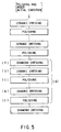
- FIG. 5 is a flowchart of polishing and dressing, which is in accordance with the passage of time. It is necessary to condition the polishing pad which has never been used and are made from a polyurethane foam, because it has the same rough surface state as that after being diamond-dressed.
- the ceramic dresser according to the present invention can serve both as dressing and conditioning treatments.
- the polishing pad which has never been used is dressed with the ceramic dresser (i.e., ceramic-dressing).
- ceramic dresser i.e., ceramic-dressing
- this polishing pad for example, from one to six silicon wafers are polished (i.e., wafer-polishing).
- the ceramic-dressing/wafer-dressing is repeated plural times.
- the above is a polishing/dressing sequence in the case of using a polishing pad which has never been used.
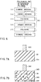
- the following will describe the second embodiment relating to a method for dressing a polishing pad, referring to FIG. 6.
- This embodiment is concerned with a method for dressing a polishing pad having a polishing performance deteriorated by repeated polishing.
- the polishing pad whose polishing performance is deteriorated is dressed with a diamond dresser (diamond-dressing).
- This polishing pad is then dressed with a ceramic dresser (ceramic-dressing/conditioning).
- One or more silicon wafers are polished with this polishing pad.
- the ceramic-dressing/polishing is repeated plural times.
- this polishing pad is again subjected to ceramic-dressing, and subsequently one or more silicon wafers are polished.
- This sequential process (shown in FIG. 5A) is carried out one or more times.
- FIGS. 7A and 7B, and FIGS. 8A and 8B are cross sections of dressers, respectively.
- a ceramic dresser 22 shown in FIG. 7A comprises a ceramic made by sintering alumina, silicon nitride, silicon carbide or the like at a high temperature, and has a shape of, for example, a disc. Its first principal face constitutes a dressing face 221 for dressing a polishing pad. If the dressing face has at least one step, polishing efficiency is raised. The step has a height from about 20 to 30 nm.
- the ceramic dresser 22 is operated by a supporting arm 222 fixed on a principal face opposite to the dressing face 221.
- a diamond dresser 24 shown in FIG. 7B is, for example, a disc in which diamond particles 243 are incorporated into a resin.
- a dressing face 241 has exposed sharp tips of the diamond particles 243.
- the diamond dresser 24 is operated by a supporting arm 242 fixed on an opposite face to the dressing face 241.
- the diamond particles may be incorporated into a disc formed by Ni-electrodepositing.
- FIGS. 8A and 8B are discs which may be used instead of the diamond dresser illustrated in FIG. 7B, respectively. In the dresser shown in FIG.
- a thin layer 271 which is composed of silicon nitride or silicon carbide and has a thickness from 5 to 40 ⁇ m is deposited on a surface of a silicon nitride (SiN) substrate having a thickness from 5 to 10 mm by ECR (Electron Cyclotron Resonance)-CVD.
- the surface on which this thin layer is deposited is a dressing face.
- This dresser 27 is operated by a supporting arm 272 fixed on an opposite face to the dressing face. In a dresser 28 shown in FIG.
- a thin layer 281 which is composed of silicon nitride or silicon carbide and has a thickness from 5 to 40 ⁇ m is deposited on a surface of a silicon carbide (SiC) substrate having a thickness from 5 to 10 mm by ECR-CVD.
- SiC silicon carbide
- This dresser 28 is operated by a supporting arm 282 fixed on an opposite face to the dressing face.
- dressing and polishing are repeated reciprocally (i.e. ⁇ dressing ⁇ polishing ⁇ dressing ⁇ ...) in the dressing apparatus illustrated in FIG. 2.
- FIGS. 9 and 10 are plan views of the main portions of the dressing apparatus shown in FIG. 2, respectively.
- a polishing pad 9 is set up on a polishing plate 17 which can rotate at 100 rpm.
- the number of rotation of the polishing plate 7 is usually from 20 to 200 rpm, and the pressure for pressing a silicon wafer 20 is usually from 50 to 500 g/cm 2, and preferably is about 350 g/cm 2 .
- the silicon wafer 20 is polished while it is pressed against the rotating polishing pad 19 at a given pressure.
- the polishing pad 18 is being dressed, during polishing the silicon wafer 20, by means of following the track of the silicon wafer 20 on the polishing pad 18 with use of a ceramic dresser 22 while pressing the ceramic dresser 22 against the polishing pad 18.
- the life time of the polishing pad becomes longer and the time for manufacturing a semiconductor apparatus is shortened because polishing and dressing are repeated for one silicon wafer by one silicone wafer.
- FIGS. 11A and 11B - FIGS. 14A and 14B the following will explain the state of a polishing pad to which the dressing treatment of the preset invention is applied.
- FIGS. 11A and 11B are enlarged plan view and cross section of a polishing pad which has not yet been used, respectively.
- FIGS. 12A and 12B, as well as FIGS. 13A and 13B, and FIGS. 14A and 14B, are enlarged plan view and cross section of the surface of a dressed polishing pad, respectively.
- a pore layer is formed substantially uniformly and is active.
- FIGS. 12A and 12B reaction products and particles of a polishing material are pressed and confined into the interior of the pore layer, as shown in FIGS. 12A and 12B.
- many pores of the pore layer are blocked as shown by slanting lines in FIGS. 12A and 12B.
- the pore layer comes to have no room into which the polishing material is put, so that the polishing property is reduced.
- FIGS. 14A and 14B illustrate the states after the polishing pad shown in FIGS. 12A and 12B is dressed with a ceramic dresser. The polishing pad is satisfactorily restored for a short time by only dressing treatment with the ceramic dresser.
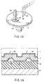
- FIG. 15 is a perspective view of a portion of a polishing apparatus which is used in this method.
- This polishing apparatus has a rotatable polishing plate 17 on which a polishing pad 19 is set up, in the same manner as in the polishing apparatus shown in FIG. 2.
- the silicon wafer (not shown in FIG. 15) fixed on the adsorbing disc 33 is rotated, for example, under a condition that the polishing surface on which a polysilicon film is formed is pressed against the polishing pad 19 by pressure.
- the polishing material may be an alkaline solution containing polishing particles such as silica.
- the alkalne solution may be a material for chemically etching silicon, for example, an organic amine.
- the additive includes cellulose such as hydroxyethyl cellulose, poly-saccharide, poly-vinyl pyrrolidone, and pyrrolidone.
- the amount of the additive is appropriately from 1 to 10 percentages by weight of the polishing material.
- a solvent for dissolving hydrophilic polysaccharide or the like includes ammonia and triethanol amine.
- FIGS. 16 and 17 are cross sections of a semiconductor substrate for explaining treatment for polishing a film to be polished of the semiconductor (e.g., silicon) substrate with a polishing pad.
- the semiconductor e.g., silicon
- a polishing material 34 into which an additive such as hydroxyethyl cellulose is added is being put into concave portions of a polysilicon film 3 formed on a silicon oxide film 2 on a semiconductor substrate 1, so that the polysilicon film 3 is being polished.
- hydroxyethyl cellulose adheres onto an uneven surface of the polysilicon film 3 so as to form a film 36.
- the film 36 is polished, from its convex portions, with the polishing pad 19 and polishing particles in the polishing material so as to be removed off. As a result, only convex portions of the polysilicon film 3 are exposed.
- the exposed portions of the polysilicon film 3 are polished with the polishing pad 19 and the polishing particles while being chemically etched with the alkaline solution.
- concave portions of the film 36 portions remain as they are so that with them the concave portions of the polysilicon film 3 are covered.
- the concave portions are protected from chemical etching with the alkaline solution by the concave cover portions of the film 36 portions.
- the silicon wafer is dressed with the ceramic dresser, which is a feature of the present invention.
- Either dresser shown in FIG. 7A or FIG. 7B may be used.
- FIGS. 18A and 18B Next, the effect of this embodiment will be described, referring to FIGS. 18A and 18B.
- the polishing pad is conditioned with the ceramic dresser in every time for treating one wafer, the polishing property of the pad can be maintained stablely.
- Dressing with the ceramic dresser makes it possible to control dishing than dressing with the diamond dresser, and to control dust adhesion on the semiconductor wafer resulted from dust-generation from the polishing pad than a process without any dressing process (FIG. 18A). Longer life time of the polishing pad and stability of the polishing rate can be also expected.
- the additive, used in this embodiment, for forming a film on the surface of silicon is not limited to hydrophilic polysaccharide, and may be any material for preventing excess polishing.
- a material for oxidizing the surface of silicon may be used.
- a Si 3 N 4 film 7 is deposited on a semiconductor substrate 1 by, for example, CVD (FIG. 19A). Specified portions of the a Si 3 N 4 film 7 and the semiconductor substrate 1 are then etched by patterning to form grooves 8 in these portions (FIG. 19B). A SiO 2 film 5 is deposited on the Si 3 N 4 and in the grooves 8 by CVD (FIG. 20A). Subsequently, the SiO 2 film is polished by the CMP process.
- the polishing treatment of the SiO 2 film 5 is stopped, thereby finishing to embed the SiO 2 film into the grooves 8 and making the surface of the semiconductor substrate 1 flat (FIG. 20B).
- the dressing treatment which is a feature of the present invention is applied to the polishing pad.
- This dressing treatment causes the polishing pad deteriorated by polishing the silicon wafers to be restored for a short time.
- FIGS. 21A and 21B are cross sections of a structure of an apparatus used in the method of manufacturing a semiconductor device, to which the step of separating trench elements is applied.
- the surface of a semiconductor substrate 1 is oxidized by heat to form a SiO 2 film 2, and then a Si 3 N 4 film 7, which is a stopper layer for stopping polishing, is deposited on the SiO 2 film by CVD.
- parts of the Si 3 N 4 film7, the SiO 2 film 2 and the semiconductor substrate 1, the parts being areas for forming elements separately, are removed off by lithographic patterning to form grooves 9.
- the surface of the semiconductor substrate 1 is oxidized within the grooves 9, and then boron is ion-implanted onto the bottom of the groove 9 to form channel cutting areas 10.
- a polysilicon film 3 is then deposited on the Si 3 N 4 film 7 and in the grooves 9 by CVD (FIG. 21A).
- SiO 2 may be used instead of the polysilicon film.
- the polysilicon film 3 on the surface of the semiconductor substrate 1 is polished until the Si 3 N 4 film 7 is exposed (FIG. 21B).
- the polishing rate of the Si 3 N 4 film 7 is about from one-tenth to one-two hundredth as low as that of the polysilicon film and consequently the polishing treatment can be stopped by the Si 3 N 4 film 7, so that the polysilicon film 3 can be embedded only in the grooves.
- a layer whose polishing rate is smaller than a layer to be polished can be selected as the stopper film for stopping polishing, and the polishing time can be specified.
- the polishing treatment can be stopped when the stopper film is exposed.
- the dressing treatment which is a feature of the present invention is applied to the polishing pad.
- This dressing treatment causes the polishing pad deteriorated by polishing the silicon wafers to be restored for a short time.
- the seventh embodiment which relates to a polishing process used in the case of embedding a metallic wiring into grooves of an insulated film.
- a SiO 2 film 5 and a plasma SiO 2 film 12 are deposited on a semiconductor substrate 1 in sequence by CVD (FIG. 22A). Specified portions of the plasma SiO 2 film 12 are then patterned to form grooves 14 (FIG. 22B). A Cu film 16 is deposited into the grooves 14 and on the whole surface of the plasma SiO 2 film 12 (FIG. 22C). The Cu film 16 is polished, with use of the plasma SiO 2 film 12 as a stopper film. When the plasma SiO 2 film is exposed, the polishing treatment of the Cu film 16 is stopped, so that the Cu film 16 is embedded only in the grooves 14 to form a Cu embedded wiring (FIG. 23A).
- This polishing makes the surface of the semiconductor substrate 1 flat, and consequently the formation of the subsequent, second plasma SiO 2 film is easy (FIG. 23B). Because of the flatness according to CMP process, the formation of electrode wiring (not shown) of second film and third film will be easy.
- the dressing treatment which is a feature of the present invention is applied to the polishing pad.
- This dressing treatment causes the polishing pad deteriorated by polishing the silicon wafers to be restored for a short time.
Landscapes
- Engineering & Computer Science (AREA)
- Mechanical Engineering (AREA)
- Mechanical Treatment Of Semiconductor (AREA)
- Finish Polishing, Edge Sharpening, And Grinding By Specific Grinding Devices (AREA)
- Grinding-Machine Dressing And Accessory Apparatuses (AREA)
Applications Claiming Priority (3)
| Application Number | Priority Date | Filing Date | Title |
|---|---|---|---|
| JP10680497A JP3676030B2 (ja) | 1997-04-10 | 1997-04-10 | 研磨パッドのドレッシング方法及び半導体装置の製造方法 |
| JP106804/97 | 1997-04-10 | ||
| JP10680497 | 1997-04-10 |
Publications (3)
| Publication Number | Publication Date |
|---|---|
| EP0870577A2 true EP0870577A2 (de) | 1998-10-14 |
| EP0870577A3 EP0870577A3 (de) | 1998-11-18 |
| EP0870577B1 EP0870577B1 (de) | 2003-01-15 |
Family
ID=14443056
Family Applications (1)
| Application Number | Title | Priority Date | Filing Date |
|---|---|---|---|
| EP98106638A Expired - Lifetime EP0870577B1 (de) | 1997-04-10 | 1998-04-09 | Verfahren zum Abrichten eines Polierkissens. |
Country Status (5)
| Country | Link |
|---|---|
| US (2) | US6241581B1 (de) |
| EP (1) | EP0870577B1 (de) |
| JP (1) | JP3676030B2 (de) |
| KR (1) | KR100264756B1 (de) |
| DE (1) | DE69810686T2 (de) |
Cited By (5)
| Publication number | Priority date | Publication date | Assignee | Title |
|---|---|---|---|---|
| GB2345256A (en) * | 1998-06-29 | 2000-07-05 | Nec Corp | Polishing apparatus |
| WO2001003886A1 (en) * | 1999-07-09 | 2001-01-18 | Speedfam-Ipec Corporation | Method and apparatus for eliminating wear and grooving of workpiece carrier retaining element |
| EP1125688A4 (de) * | 1998-10-28 | 2006-09-27 | Hitachi Ltd | Poliervorrichtung und halbleiter-herstellungsverfahren unter verwendung desselben |
| US7166013B2 (en) | 1998-10-28 | 2007-01-23 | Hitachi, Ltd. | Polishing apparatus and method for producing semiconductors using the apparatus |
| WO2013089502A1 (en) * | 2011-12-16 | 2013-06-20 | Lg Siltron Inc. | Apparatus and method for polishing wafer |
Families Citing this family (26)
| Publication number | Priority date | Publication date | Assignee | Title |
|---|---|---|---|---|
| US6372648B1 (en) * | 1998-11-16 | 2002-04-16 | Texas Instruments Incorporated | Integrated circuit planarization method |
| JP4501694B2 (ja) * | 1998-12-25 | 2010-07-14 | 日立化成工業株式会社 | Cmp研磨剤用添加液 |
| KR20050006299A (ko) * | 1998-12-25 | 2005-01-15 | 히다치 가세고교 가부시끼가이샤 | Cmp 연마제, cmp 연마제용 첨가액 및 기판의 연마방법 |
| JP4604727B2 (ja) * | 1998-12-25 | 2011-01-05 | 日立化成工業株式会社 | Cmp研磨剤用添加液 |
| KR20010004982A (ko) * | 1999-06-30 | 2001-01-15 | 김영환 | 반도체 소자의 산화막 연마용 슬러리 제조 방법 |
| JP3760064B2 (ja) * | 1999-08-09 | 2006-03-29 | 株式会社日立製作所 | 半導体装置の製造方法及び半導体装置の平坦化加工装置 |
| JP2001077060A (ja) * | 1999-09-08 | 2001-03-23 | Toshiba Corp | 半導体装置の製造方法 |
| JP2001274122A (ja) * | 2000-03-23 | 2001-10-05 | Tokyo Seimitsu Co Ltd | ウェハ研磨装置 |
| US6752697B1 (en) * | 2000-08-23 | 2004-06-22 | Advanced Micro Devices, Inc. | Apparatus and method for chemical mechanical polishing of a substrate |
| JP2002170792A (ja) * | 2000-11-29 | 2002-06-14 | Mitsubishi Electric Corp | 研磨液供給装置及び研磨液供給方法、研磨装置及び研磨方法、並びに、半導体装置の製造方法 |
| DE10162597C1 (de) * | 2001-12-19 | 2003-03-20 | Wacker Siltronic Halbleitermat | Verfahren zur Herstellung beidseitig polierter Halbleiterscheiben |
| DE10241300A1 (de) * | 2002-09-04 | 2004-03-18 | Merck Patent Gmbh | Ätzpasten für Siliziumoberflächen und -schichten |
| WO2004062851A1 (ja) * | 2003-01-15 | 2004-07-29 | Mitsubishi Materials Corporation | 軟質材加工用切削工具 |
| US20040192178A1 (en) * | 2003-03-28 | 2004-09-30 | Barak Yardeni | Diamond conditioning of soft chemical mechanical planarization/polishing (CMP) polishing pads |
| JP2005217037A (ja) * | 2004-01-28 | 2005-08-11 | Asahi Sunac Corp | 半導体ウェーハ用研磨パッドのコンディショニング方法 |
| JP2005262406A (ja) * | 2004-03-19 | 2005-09-29 | Toshiba Corp | 研磨装置および半導体装置の製造方法 |
| US7070484B2 (en) * | 2004-05-21 | 2006-07-04 | Mosel Vitelic, Inc. | Pad break-in method for chemical mechanical polishing tool which polishes with ceria-based slurry |
| KR100678303B1 (ko) * | 2004-05-25 | 2007-02-02 | 동부일렉트로닉스 주식회사 | 화학 기계적 연마(cmp) 패드 드레서 및 화학 기계적연마(cmp) 장치 |
| US20060211237A1 (en) * | 2005-03-21 | 2006-09-21 | Taiwan Semiconductor Manufacturing Co., Ltd. | Method and apparatus for planarizing gap-filling material |
| JP5444596B2 (ja) * | 2007-08-31 | 2014-03-19 | 富士通セミコンダクター株式会社 | 半導体装置の製造方法 |
| JP5149020B2 (ja) * | 2008-01-23 | 2013-02-20 | 株式会社ディスコ | ウエーハの研削方法 |
| JP2011071303A (ja) * | 2009-09-25 | 2011-04-07 | Toshiba Corp | 半導体装置の製造方法 |
| CN102140030B (zh) * | 2010-02-02 | 2013-01-23 | 中国科学院理化技术研究所 | 无需烧结制备高气孔率纳米晶碳化硅泡沫陶瓷的方法 |
| KR101211138B1 (ko) * | 2011-03-07 | 2012-12-11 | 이화다이아몬드공업 주식회사 | 연약패드용 컨디셔너 및 그 제조방법 |
| JP5733623B2 (ja) * | 2011-06-10 | 2015-06-10 | 国立大学法人九州大学 | 半導体装置の製造方法 |
| EP3053704A4 (de) * | 2013-10-04 | 2017-07-19 | Fujimi Incorporated | Poliervorrichtung, verarbeitungsverfahren für ein polierelement, verfahren zur modifikation des polierelements, formverarbeitendes schneidwerkzeug und oberflächenmodifikationswerkzeug |
Family Cites Families (16)
| Publication number | Priority date | Publication date | Assignee | Title |
|---|---|---|---|---|
| JPS56152562A (en) * | 1980-04-24 | 1981-11-26 | Fujitsu Ltd | Grinder |
| EP0322721B1 (de) * | 1987-12-29 | 1993-10-06 | E.I. Du Pont De Nemours And Company | Feine Polierzusammensetzung für Plaketten |
| JPH07237120A (ja) * | 1994-02-22 | 1995-09-12 | Nec Corp | ウェーハ研磨装置 |
| JP2914166B2 (ja) * | 1994-03-16 | 1999-06-28 | 日本電気株式会社 | 研磨布の表面処理方法および研磨装置 |
| JP3278532B2 (ja) * | 1994-07-08 | 2002-04-30 | 株式会社東芝 | 半導体装置の製造方法 |
| US5536202A (en) * | 1994-07-27 | 1996-07-16 | Texas Instruments Incorporated | Semiconductor substrate conditioning head having a plurality of geometries formed in a surface thereof for pad conditioning during chemical-mechanical polish |
| JP2647050B2 (ja) * | 1995-03-31 | 1997-08-27 | 日本電気株式会社 | ウェハ研磨装置 |
| JP3778594B2 (ja) * | 1995-07-18 | 2006-05-24 | 株式会社荏原製作所 | ドレッシング方法 |
| JP3111892B2 (ja) * | 1996-03-19 | 2000-11-27 | ヤマハ株式会社 | 研磨装置 |
| US5890951A (en) * | 1996-04-15 | 1999-04-06 | Lsi Logic Corporation | Utility wafer for chemical-mechanical planarization |
| JP3507628B2 (ja) * | 1996-08-06 | 2004-03-15 | 昭和電工株式会社 | 化学的機械研磨用研磨組成物 |
| JP3679882B2 (ja) * | 1997-02-07 | 2005-08-03 | 株式会社荏原製作所 | 研磨用クロスのドレッサー及びその製造方法 |
| JPH10329007A (ja) * | 1997-05-28 | 1998-12-15 | Sony Corp | 化学的機械研磨装置 |
| JPH11188626A (ja) * | 1997-12-26 | 1999-07-13 | Narumi China Corp | セラミックスドレス基板 |
| US6123607A (en) * | 1998-01-07 | 2000-09-26 | Ravkin; Michael A. | Method and apparatus for improved conditioning of polishing pads |
| US5941762A (en) * | 1998-01-07 | 1999-08-24 | Ravkin; Michael A. | Method and apparatus for improved conditioning of polishing pads |
-
1997
- 1997-04-10 JP JP10680497A patent/JP3676030B2/ja not_active Expired - Fee Related
-
1998
- 1998-04-07 US US09/055,944 patent/US6241581B1/en not_active Expired - Lifetime
- 1998-04-09 DE DE69810686T patent/DE69810686T2/de not_active Expired - Lifetime
- 1998-04-09 EP EP98106638A patent/EP0870577B1/de not_active Expired - Lifetime
- 1998-04-10 KR KR1019980012746A patent/KR100264756B1/ko not_active Expired - Fee Related
-
2001
- 2001-04-23 US US09/839,240 patent/US6716087B2/en not_active Expired - Lifetime
Cited By (7)
| Publication number | Priority date | Publication date | Assignee | Title |
|---|---|---|---|---|
| GB2345256A (en) * | 1998-06-29 | 2000-07-05 | Nec Corp | Polishing apparatus |
| GB2345256B (en) * | 1998-06-29 | 2002-01-16 | Nec Corp | Polishing apparatus |
| EP1125688A4 (de) * | 1998-10-28 | 2006-09-27 | Hitachi Ltd | Poliervorrichtung und halbleiter-herstellungsverfahren unter verwendung desselben |
| US7137866B2 (en) | 1998-10-28 | 2006-11-21 | Hitachi Ltd. | Polishing apparatus and method for producing semiconductors using the apparatus |
| US7166013B2 (en) | 1998-10-28 | 2007-01-23 | Hitachi, Ltd. | Polishing apparatus and method for producing semiconductors using the apparatus |
| WO2001003886A1 (en) * | 1999-07-09 | 2001-01-18 | Speedfam-Ipec Corporation | Method and apparatus for eliminating wear and grooving of workpiece carrier retaining element |
| WO2013089502A1 (en) * | 2011-12-16 | 2013-06-20 | Lg Siltron Inc. | Apparatus and method for polishing wafer |
Also Published As
| Publication number | Publication date |
|---|---|
| EP0870577A3 (de) | 1998-11-18 |
| US6241581B1 (en) | 2001-06-05 |
| KR100264756B1 (ko) | 2000-09-01 |
| US6716087B2 (en) | 2004-04-06 |
| DE69810686T2 (de) | 2003-09-18 |
| EP0870577B1 (de) | 2003-01-15 |
| JPH10286756A (ja) | 1998-10-27 |
| DE69810686D1 (de) | 2003-02-20 |
| US20010029156A1 (en) | 2001-10-11 |
| JP3676030B2 (ja) | 2005-07-27 |
| KR19980081281A (ko) | 1998-11-25 |
Similar Documents
| Publication | Publication Date | Title |
|---|---|---|
| US6241581B1 (en) | Method for dressing a polishing pad, polishing apparatus, and method for manufacturing a semiconductor apparatus | |
| US6994611B2 (en) | Method and system for cleaning a chemical mechanical polishing pad | |
| JP3645528B2 (ja) | 研磨方法及び半導体装置の製造方法 | |
| US5702563A (en) | Reduced chemical-mechanical polishing particulate contamination | |
| JP3120280B2 (ja) | 機械化学的研摩方法及びその装置 | |
| US5957757A (en) | Conditioning CMP polishing pad using a high pressure fluid | |
| JP2943981B2 (ja) | 半導体ウェーハ用研磨パッドおよび研磨方法 | |
| KR100509659B1 (ko) | 반도체장치기판연마공정 | |
| US6431960B1 (en) | Fixed abrasive polishing pad | |
| JP3438383B2 (ja) | 研磨方法およびこれに用いる研磨装置 | |
| US20010000586A1 (en) | Technique for chemical mechanical polishing silicon | |
| US6218306B1 (en) | Method of chemical mechanical polishing a metal layer | |
| US6390902B1 (en) | Multi-conditioner arrangement of a CMP system | |
| US6517416B1 (en) | Chemical mechanical polisher including a pad conditioner and a method of manufacturing an integrated circuit using the chemical mechanical polisher | |
| TW200919572A (en) | Method of soft pad preparation to reduce removal rate ramp-up effect and to stabilize defect rate | |
| US6478977B1 (en) | Polishing method and apparatus | |
| WO2002028596A1 (en) | Web-style pad conditioning system and methods for implementing the same | |
| US20220297258A1 (en) | Substrate polishing simultaneously over multiple mini platens | |
| JP2002299289A (ja) | 化学的機械的研磨方法および半導体装置の製造方法 | |
| US20090130958A1 (en) | Fixed Abrasive Pad Having Different Real Contact Areas and Fabrication Method Thereof | |
| KR200274610Y1 (ko) | 드레싱 단계를 개선시킨 화학기계연마장치 | |
| JP2000173958A (ja) | 半導体装置の製造方法及び半導体製造装置 | |
| KR20060075453A (ko) | 연마 패드의 컨디셔닝 방법 | |
| KR20070024145A (ko) | 반도체 디바이스 제조를 위한 씨엠피 장치 | |
| KR20000015120A (ko) | Cmp용 인서트 필름의 컨디셔닝 방법 |
Legal Events
| Date | Code | Title | Description |
|---|---|---|---|
| PUAI | Public reference made under article 153(3) epc to a published international application that has entered the european phase |
Free format text: ORIGINAL CODE: 0009012 |
|
| PUAL | Search report despatched |
Free format text: ORIGINAL CODE: 0009013 |
|
| 17P | Request for examination filed |
Effective date: 19980409 |
|
| AK | Designated contracting states |
Kind code of ref document: A2 Designated state(s): DE FR GB |
|
| AX | Request for extension of the european patent |
Free format text: AL;LT;LV;MK;RO;SI |
|
| AK | Designated contracting states |
Kind code of ref document: A3 Designated state(s): AT BE CH CY DE DK ES FI FR GB GR IE IT LI LU MC NL PT SE |
|
| AX | Request for extension of the european patent |
Free format text: AL;LT;LV;MK;RO;SI |
|
| AKX | Designation fees paid |
Free format text: DE FR GB |
|
| 17Q | First examination report despatched |
Effective date: 20010320 |
|
| GRAG | Despatch of communication of intention to grant |
Free format text: ORIGINAL CODE: EPIDOS AGRA |
|
| RTI1 | Title (correction) |
Free format text: METHOD FOR DRESSING A POLISHING PAD. |
|
| GRAG | Despatch of communication of intention to grant |
Free format text: ORIGINAL CODE: EPIDOS AGRA |
|
| GRAH | Despatch of communication of intention to grant a patent |
Free format text: ORIGINAL CODE: EPIDOS IGRA |
|
| GRAH | Despatch of communication of intention to grant a patent |
Free format text: ORIGINAL CODE: EPIDOS IGRA |
|
| GRAA | (expected) grant |
Free format text: ORIGINAL CODE: 0009210 |
|
| AK | Designated contracting states |
Kind code of ref document: B1 Designated state(s): DE FR GB |
|
| REG | Reference to a national code |
Ref country code: GB Ref legal event code: FG4D |
|
| REF | Corresponds to: |
Ref document number: 69810686 Country of ref document: DE Date of ref document: 20030220 Kind code of ref document: P |
|
| ET | Fr: translation filed | ||
| PLBE | No opposition filed within time limit |
Free format text: ORIGINAL CODE: 0009261 |
|
| STAA | Information on the status of an ep patent application or granted ep patent |
Free format text: STATUS: NO OPPOSITION FILED WITHIN TIME LIMIT |
|
| 26N | No opposition filed |
Effective date: 20031016 |
|
| PGFP | Annual fee paid to national office [announced via postgrant information from national office to epo] |
Ref country code: DE Payment date: 20150331 Year of fee payment: 18 Ref country code: GB Payment date: 20150408 Year of fee payment: 18 |
|
| REG | Reference to a national code |
Ref country code: FR Ref legal event code: PLFP Year of fee payment: 19 |
|
| PGFP | Annual fee paid to national office [announced via postgrant information from national office to epo] |
Ref country code: FR Payment date: 20160309 Year of fee payment: 19 |
|
| REG | Reference to a national code |
Ref country code: DE Ref legal event code: R119 Ref document number: 69810686 Country of ref document: DE |
|
| GBPC | Gb: european patent ceased through non-payment of renewal fee |
Effective date: 20160409 |
|
| PG25 | Lapsed in a contracting state [announced via postgrant information from national office to epo] |
Ref country code: DE Free format text: LAPSE BECAUSE OF NON-PAYMENT OF DUE FEES Effective date: 20161101 Ref country code: GB Free format text: LAPSE BECAUSE OF NON-PAYMENT OF DUE FEES Effective date: 20160409 |
|
| REG | Reference to a national code |
Ref country code: FR Ref legal event code: ST Effective date: 20171229 |
|
| PG25 | Lapsed in a contracting state [announced via postgrant information from national office to epo] |
Ref country code: FR Free format text: LAPSE BECAUSE OF NON-PAYMENT OF DUE FEES Effective date: 20170502 |