EP0871139A2 - Seriendrucker und Bildpufferzugriffsverfahren für einen Seriendrucker - Google Patents
Seriendrucker und Bildpufferzugriffsverfahren für einen Seriendrucker Download PDFInfo
- Publication number
- EP0871139A2 EP0871139A2 EP98301778A EP98301778A EP0871139A2 EP 0871139 A2 EP0871139 A2 EP 0871139A2 EP 98301778 A EP98301778 A EP 98301778A EP 98301778 A EP98301778 A EP 98301778A EP 0871139 A2 EP0871139 A2 EP 0871139A2
- Authority
- EP
- European Patent Office
- Prior art keywords
- data
- image buffer
- image data
- serial printer
- stored
- Prior art date
- Legal status (The legal status is an assumption and is not a legal conclusion. Google has not performed a legal analysis and makes no representation as to the accuracy of the status listed.)
- Granted
Links
Images


Classifications
-
- G—PHYSICS
- G06—COMPUTING OR CALCULATING; COUNTING
- G06K—GRAPHICAL DATA READING; PRESENTATION OF DATA; RECORD CARRIERS; HANDLING RECORD CARRIERS
- G06K15/00—Arrangements for producing a permanent visual presentation of the output data, e.g. computer output printers
- G06K15/02—Arrangements for producing a permanent visual presentation of the output data, e.g. computer output printers using printers
- G06K15/10—Arrangements for producing a permanent visual presentation of the output data, e.g. computer output printers using printers by matrix printers
-
- G—PHYSICS
- G06—COMPUTING OR CALCULATING; COUNTING
- G06K—GRAPHICAL DATA READING; PRESENTATION OF DATA; RECORD CARRIERS; HANDLING RECORD CARRIERS
- G06K2215/00—Arrangements for producing a permanent visual presentation of the output data
- G06K2215/0002—Handling the output data
- G06K2215/0077—Raster outputting to the print element(s)
-
- G—PHYSICS
- G06—COMPUTING OR CALCULATING; COUNTING
- G06K—GRAPHICAL DATA READING; PRESENTATION OF DATA; RECORD CARRIERS; HANDLING RECORD CARRIERS
- G06K2215/00—Arrangements for producing a permanent visual presentation of the output data
- G06K2215/0082—Architecture adapted for a particular function
- G06K2215/0094—Colour printing
Definitions
- the present invention relates to a serial printer that is employed in a computer system as a terminal printer or a facsimile terminal, and in particular to a serial printer that employs an improved method for storing data in an image buffer.
- a conventional serial printer generates an interrupt for each printing sequence, and in accordance with an interrupt process program, transmits required image data from a buffer (an image buffer), in which they are stored, to a print head.
- a buffer an image buffer
- a print head Provided in the print head are a plurality of dot formation elements (e.g., ink-jet nozzles or impact wires) that are arranged in the columnar direction (perpendicularly), and as the head is moved across a row (horizontally), the dot formation element array is activated each time it reaches the position of an individual pixel.
- dot formation elements e.g., ink-jet nozzles or impact wires
- Fig. 10 is a diagram showing how to handle data stored in the image buffer of the serial printer.
- Source data for input to a serial printer are first stored to a memory area called a data buffer 61.
- the source data can include various types of image data; thus, in the example shown in Fig. 10, for easy understanding of what is defined as last image data 69 that is held in an image buffer 67, which will be described later, raster graphics image data 65, which correspond to the last image data 69, are stored that are supposed to be included in the source data.
- the individual blocks denoted by numerals 1, 2 and 3 in the source image data 65 represent the data for one byte (a set of eight sequential pixels on the same line) .
- the numbers provided for the bytes indicate the order in which an image has been scanned using the raster method.
- rater scanning begins at the topmost line (horizontal line) in an image, and scans the pixels in this line horizontally from the left to the right (or in the reverse direction) (byte 1 to byte 10 in Fig. 10), and then scans the second line horizontally (byte 11 to byte 20) and moves to the line immediately below. This process is repeated until the scanning is completed for the bottom line.
- the source data 65 read from the data buffer 61 are employed to generate the last raster graphics image data 69, which are written in the image buffer 67.
- the order in which the last image data 69 is generated corresponds to the above described raster scanning order (i.e., the order following the byte numbers in Fig. 10), while the order in which the image buffer 67 is accessed when the data is written corresponds simply to the address order. Therefore, the last image data 69 are so stored in the image buffer 67 that, as is shown in Fig. 10, when data in the image buffer 67 are accessed in the order of the addresses, the bytes are read in the raster order (in the ascending number order).
- the bytes of the last image data 69 are read from the image buffer 67 and are transmitted to the print head.
- the order in which the bytes are read from the image buffer 67 corresponds to the order in which the dot formation elements are arranged in the sub-scanning direction of the print head, which does not match the raster scanning order.
- the general print head for a serial printer has a plurality of dot formation elements (e.g., ink-jet nozzles or impact wires) that are arranged in the sub-scanning direction (the columnar direction), and while the head is moving in the main scanning direction (along a row), the dot formation element array must be activated each time it reaches the location of an individual pixel.
- a set of a plurality of bytes that are to be given to the dot formation element array i.e., a plurality of bytes that are arranged in the image buffer 67 in the columnar direction, must be read.
- a set of four bytes, bytes 1, 11, 21 and 31, is read, then a set of bytes 2, 12, 22 and 32, is read, and finally a set of bytes 3, 13, 23 and 33 is read.
- the bytes that are to be read as a set are stored at addresses that are located separate from another in the image buffer 67.
- Fig. 11(a) is shown the schematic arrangement for a print head, in a serial in-jet color printer, though which ink is ejected.
- a print head 54 there are four nozzle arrays 71, 72, 73 and 74.
- a plurality of nozzles 71a, 72a, 73a and 74a are provided for each of the nozzle arrays 71, 72, 73 and 74.
- the arrangement for the nozzle arrays 71, 72, 73 and 74 is so designed that the arrays are separated by a predetermined distance d.
- differently colored inks such as cyan (C), magenta (M), yellow (Y) and black (K) are allocated for the nozzle arrays 71, 72, 73 and 74, and C, M, Y and K dots are printed at the same location for mixing the colors.
- Fig. 11(b) when the print head 54 is located at position (A), the ink is ejected through the nozzle array 71, and when the print head 54 is located at position (B), the ink is ejected through the nozzle array 72. Similarly, when the print head 54 is located at position (C), the ink is ejected through the nozzle array 73, and when the print head 54 is located at position (D), the ink is ejected through the nozzle array 74.
- the print head of the color ink-jet printer is so designed that, for example, ink-jet nozzle arrays for four colors, cyan (C), magenta (M), yellow (Y) and black (K), each array including a plurality of nozzles (five nozzles in Fig. 11), are located at a predetermined interval d.
- ink-jet nozzle arrays for four colors cyan (C), magenta (M), yellow (Y) and black (K), each array including a plurality of nozzles (five nozzles in Fig. 11)
- C cyan
- M magenta
- Y yellow
- K black
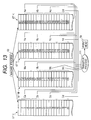
- Fig. 12 is shown a method, employed by a conventional serial color printer, for storing data in an image buffer.
- an image buffer 67' how separate for memory areas for the individual C, M, Y and K color nozzle arrays.
- data are stored for each of the C, M, Y and K nozzle arrays, with sets of data in the memory being provided for each nozzle array in a count equivalent to the number of nozzles.
- the above described data for eight horizontal bits are stored discontinuously for each C, M, Y or K nozzle array.
- portion d' corresponds to the memory value that corresponds to the predetermined distance d separating the nozzle arrays shown in Fig. 11, and the actual image (printing) area in the memory is as is shown in Fig. 12(a).
- data are extracted, in order, from the C, M, Y and K memory areas in the image buffer 67' as is shown in Fig. 12(b), and are transmitted to the print head.
- a plurality of bytes which are arranged in the direction of rows in the memory area for each color that corresponds to one nozzle array, are read as a set from the image buffer 67' and are transmitted to the print head.
- the data for one column are transmitted to the print head in consonance with at a specific print timing.
- the C, M, Y and K color images are developed individually, and C, M, Y and K color image data respectively are stored, in that order, in memory areas 67'C, 67'M, 67'Y and 67'K in the image buffer 67', as is shown in Fig. 13.
- data for five bytes, Ca, Ma, Ya and Ka are transmitted to the print head from the C, M, Y and K color memory areas 67'C, 67'M, 67'Y and 67'K, as is shown in Fig. 13.
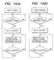
- Fig. 14 is a flowchart for the processing performed by a conventional serial color printer for transferring data to the print head using a program.
- the bytes arranged in the direction of rows are stored in memory areas at addresses that are separated from each other in the image buffer 67. In the transfer process 111, therefore, calculation of the separated addresses must be performed for each data reading.
- the transfer process 111 the time at which a set of the bytes is transferred from the image buffer 67 to the print head must be determined in consonance with the time at which the dot formation element arrays arrive at individual pixel positions.
- the transfer process is performed as an interrupt process for which a periodical signal that is generated by a carriage moving system is used as a trigger. While the transfer process must be performed at a timing that is vigorously controlled, the performance of the above described complicated address calculation increases the load imposed on the CPU, and deteriorates throughput.
- the image buffer is separated into memory areas for four colors, C, M, Y and K, as is shown in Figs. 12 and 13, and image data for four colors are discontinuously stored for individual C, M, Y and K nozzle arrays.
- the discontinuous addresses must be accessed a number of times that corresponds to the number of colors.
- the pointers for the colors C, M, Y and K must be managed independently.
- DMA may be employed for high-speed data transfer.
- the number of nozzle arrays in the serial printer is three, or may be as many as ten, and when, for example, the data are stored discontinuously for the C, M, Y and K nozzle arrays, at least four DMA transfer circuits (channels) are required to transfer data to the print head.
- a first object of the present invention to provide a serial printer that obtains continuous image data that are set, at the same printing timing, for dot formation element arrays in a print head; reduces the number of times address calculations and memory accesses times are required by transferring sets of image data; reduces the load imposed on the CPU during the data transfer; and improves the throughput.
- a serial printer stores, at continuous addresses in an image buffer, pixel values or pixel value groups of image data that are set, at the same printing timing, for a predetermined dot formation element array for a print head.
- a serial printer which includes a print head consisting of at least one dot formation element array, which performs an imaging process for generating image data which storing the image data in an image buffer and a transfer process by which the image data are transferred from the image buffer and are set in the predetermined formation element array, and which displaces the print head in a main direction and initiates printing in accordance with a predetermined printing timing, wherein a pixel value or pixel value groups for image data, which are set at the same printing time for the predetermined dot formation element array, are stored at continuous addresses in the image buffer.
- pixel values or pixel Value groups of image data which are set at the same printing timing for a specific dot formation element array, are stored at continuous addresses in the image buffer, a set of data can be transferred for the dot formation element array at a specific printing timing, and continuity can be provided for data during the transfer.
- pixel values or pixel value groups of image data which are set for the predetermined dot formation element array at the same printing timing, are stored at continuous addresses in the image buffer.
- pixel values or pixel value groups can simply be read from the image buffer in the address order, and can be transmitted to the print head. That is, complicated address calculations are not required for the transfer process, and the time required for the transfer process is reduced. Instead, address calculations are required in the imaging process; but since no restriction concerning time is imposed on the imaging process, unlike the transfer process, the total load imposed on the CPU is reduced.
- the imaging process is originally a dispersed process, and for this process, continuous addresses are not as much required as for the transfer process. During the transfer process, only the data transfer between memories is performed, which is adequate for data transfers performed for the block units.
- pixel values or pixel value groups for image data are generated in a raster scanning order, and are stored at addresses in the image buffer that are separated by a distance corresponding to the number of dot formation elements in the sub-scanning direction.
- Such a storage method is one whereby, in the imaging process, pixel values or pixel value groups for image data are generated in a raster scanning order; whereby the pixel values or the pixel value groups for one line that are sequentially generated are stored at addresses in the image buffer that are separated by a distance corresponding to the number of dot formation elements that are arranged in a print head in the columnar direction; and whereby pixel values or pixel value groups that are sequentially generated for a subsequent line are stored at addresses following the addresses for the pixels and the pixel value group for a previous line.
- the pixel values or the pixel value groups that are sequentially arranged in the direction of rows are stored at addresses in the image buffer that are separated by a distance corresponding to the number of dot formation elements in the print head, while the pixel values or the pixel value groups that are sequentially arranged in the direction of rows are stored at continuous addresses in the image buffer.
- a serial printer changes the arrangement of data for each dot formation element array, so that when data are to be stored in the image buffer, the data can be sequentially transferred to the dot formation element arrays that are located at a distance from each other.
- the data are stored for each dot formation element array, and the number of sets of data that are provided is equivalent to the number of the dot formation element arrays.
- a data group to be transferred to a specific dot formation element array is sequentially stored at a specific timing when a data group is to be transferred at the same timing to another dot formation element array, so that the data are formed as a set for transfer at a specific print timing to the dot formation element array, and continuity of data can be established during the data transfer.
- a serial printer which has a print head consisting of a plurality of dot formation element arrays that are located in the main scanning direction at a predetermined distance from each other, which performs an imaging process for producing image data and storing the image data in an image buffer and a transfer process for transferring the image data from the image buffer to the plurality of dot formation element arrays, and which displaces the print head in the main scanning direction and initiates printing at a predetermined print timing, wherein pixel values or pixel value groups of the image data, which are set at the same print timing for each of the dot formation element arrays, are stored at continuous addresses in the image buffer.
- dummy data are stored at the predetermined interval in the image buffer, so as to access a set of pixel values or pixel value groups for the image data, which are set at the same print timing for the plurality of dot formation element arrays.
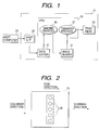
- Fig. 1 is shown the general arrangement of a serial printer, according to a first embodiment of the present invention, that is employed as a terminal printer for a computer system.
- a printer 21 receives source data from a host computer 23 via a host interface 25, and temporarily stores them in a data (reception) buffer 27.
- the source data constitutes a stream of commands that are represented in a language that the printer 21 understands, and the commands include data that represent an image using one of the above described forms.
- a CPU 29 in the printer 21 performs an imaging process 35, a transfer process 37, and various other processes.
- the imaging process 35 the source data are read from the data buffer 27 in the reception order and are translated, and raster graphics image data, which is a set of binary values indicating whether a dot should be printed for each pixel, are produced and written to an image buffer 31.
- the transfer process 37 the image data in the image buffer 31 are transferred to a print head 33.
- the transfer process is performed as an interrupt process in which a periodical signal, which is transmitted by a carriage moving system (not shown) that moves the print head 33, is employed as a trigger.
- Fig. 2 is a diagram showing the arrangement of dot formation elements in the print head 33 used in this embodiment.
- the print head 33 has five dot formation elements 39 arranged in the columnar direction.
- the print head 33 moves in the direction of rows (horizontally) along the surface of a sheet, and the five dot formation elements 39 are operated at one time when they arrive at individual pixel locations (i.e., a dot is printed or not).
- An actual print head has more dot formation elements than those shown in Fig. 2, for example, 32 dot formation elements, and in addition to the simple one array arrangement, a variety of arrangements, such as a zigzag arrangement, can be employed. Since the principle for those arrangements is the same, it would be easily understood by one having ordinary skill in the art that the principle of the present invention can be employed for a print head having a different arrangement, as well as the one in this embodiment.
- Fig. 3 is shown the writing and reading of data relative to the image buffer 31 according to this embodiment.
- Source data 41 are stored in a data buffer 27.
- the source data 41 include various forms of data that represent images; in this example, as well as in Fig. 10, the image data included in the source data 41 are raster graphics data, so as to easily understand the meaning of the last image data in the image buffer 31, which will be described later.
- Blocks numbered 1, 2, 3, . . . in the source data 41 are byte data (sets of eight continuous pixel values on the same line), and the byte number represents the raster scanning order.
- the source data 41 are read from the data buffer 27 and are translated, and last raster graphics image data 43 are produced and written to the image buffer 31.
- the bytes for the last image data 43 are produced in the raster scanning order (i.e., in the order of the byte numbers).
- the image buffer 31 is not accessed in the order of addresses, but an address is accessed that is obtained by adding the number of dot formation elements 39 (hereinafter referred to as the "height" of the print head 33), which are arranged in the columnar direction in the print head 33, to the address at which the bytes for the immediately preceding line are written.
- the first byte is written at the first address as is shown in Fig. 3, the second byte is written at an address obtained by adding a head height of "5" to the first address, and the third byte is written at an address obtained by adding another "5" to the preceding address.
- a plurality of bytes continuously arranged in the same line are stored at addresses in the image buffer 31 that are separated by a distance that is equivalent to the head height.
- bytes for the following line are stored at addresses following the addresses of the bytes for the preceding line.
- Fig. 4 is a flowchart showing the storage processing.
- steps S1 and S2 processes are performed (steps S1 and S2) for generating bytes from the source data in the raster scanning order, and a process (step S3) for calculating addresses at which to store the obtained bytes.
- the bytes are then written at the obtained addresses (step S4) .
- the above described processing is repeated for all the bands in a page image (step S5).
- a set of five bytes, 1, 11, 21, 31 and 41 are stored at the first sequential addresses; a set of following five bytes, 2, 12, 22, 32 and 42, which are arranged adjacent to the five bytes in the direction of rows, are stored at the next sequential addresses; and a set of following five bytes, 3, 13, 23, 33 and 43, are stored at the succeeding sequential addresses.
- the bytes are so arranged that the print head 33 in Fig. 2 forms dots that are stored at the sequential addresses in the image buffer 31.
- the image data 43 are read from the image buffer 31 and are transmitted to the print head 33. At this time, the data in the image buffer 31 are accessed in their addressed order. In other words, while the address is simply incremented by one, the bytes are read in order from the sequential addresses.
- the complicated address calculations are not required for the transfer process 37, and thus, the time required for the transfer processing is reduced compared to that required in the conventional case.
- Fig. 5 is a time chart showing the execution timings for the transfer processing and the processing including the imaging processing.
- the transfer processing time in this embodiment is shorter by the time required for the address calculation, as is indicated by the solid line. Accordingly, an extended time is provided for the CPU 29 for allocation for a process other than the transfer process. Since in the imaging process address calculations are increased, which is not required for the conventional art, the imaging processing time is accordingly increased.
- the scheduling is performed by a process schedular (not shown), one of the processing units in the CPU.
- a process schedular not shown
- the load imposed on the CPU is smaller than the load imposed in the conventional art, and the throughput is improved.
- scheduling be performed so that the performance of the imaging process can be set to occur during a period other than a period in which the transfer process is performed.
- a serial printer is a color ink-jet printer wherein, as well as in the above described conventional color ink-jet printer, a print head includes a plurality of ink-jet nozzle arrays, which are located at distance from each other and form dots at the same location at a predetermined print timing, using cyan, magenta, yellow and black ink droplets.
- the printer in the second embodiment is also used as a terminal printer for a computer system, and since the general arrangement is the same as that for the first embodiment in Fig. 1, no further explanation for it will be given.
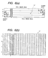
- Fig. 6 is shown a method employed by the serial printer in this embodiment for storing data in an image buffer.
- Figs. 6(a) and 6(b) in the previously described imaging process 35 performed by the serial color printer, data for C, M, Y and K color nozzle arrays are stored in the same memory area in an image buffer 31'.
- the data groups which are to be respectively transmitted to the C, M, Y and K color nozzle arrays at a specific print timing, are stored at continuous addresses in the image buffer 31', as is shown by the shaded portion in Fig. 6(a).
- a data group that is to be transferred to the C nozzle array at the same timing is stored, also stored are data groups to be transmitted to the M, Y and K color nozzle arrays at the same timing.
- a plurality of bytes (five bytes each for C, M, Y and K in the example, i.e., a total of 20 bytes), for the C, M, Y and K color nozzle arrays, which are at continuous addresses 1 to 20, are read as a data set from the image buffer 31', and at the same time are transmitted to the print head 33.
- the main feature of the serial printer of the second embodiment which has a plurality of nozzle arrays, is that a set of data is used that is to be transferred to individual nozzle arrays at a specific print timing, and continuity of data during the data transfer is provided.
- Portions d, 2d and 3d in Fig. 6(a) are memory portions that are defined the same as is explained in Fig. 12(a). As is shown in Fig. 6(b), real data are not stored in such dummy memory portions (binary "0" are stored), and there are defined as null buffers. Although the continuity of data can be obtained even without using the null buffer method, the following benefits can be obtained by using the null buffer method.
- the serial printer in this embodiment which has a plurality of nozzle arrays, employs a set of data to be transferred to individual nozzle arrays at a specific print timing, and provides continuity of data during the data transfer.
- a set of data can be transferred at a specific timing from any area in the image buffer to the individual nozzle arrays, regardless of whether the data are dummy data.
- null buffer method When the null buffer method is employed, from the programming viewpoint, extra branching is not required and the processing according to the program can be performed more easily.
- CMYK real data and dummy data need only be stored at the sequential addresses in the image buffer in the order shown in Fig. 6(b).
- the direction in which data (including dummy data) are to be extracted from the image buffer must be reversed in accordance with the printing direction.
- the direction for accessing the image buffer need only be reversed for the DMA transfer or for a data transfer performed by an interrupt process; however, a head data register for a print head, i.e., in a print ASIC, should be designed for the transmission of data to a corresponding nozzle array in either direction.
- a transfer destination address is used in common by the CMYK nozzle array, and when the data (including dummy data) are extracted from the image buffer in the reverse direction, the storage of data in the head data register is also performed in the reverse direction.
- a select switch must be provided for the print ASIC, so that the direction in which data are to be stored in the head data register is changed before the transfer of data is initiated.
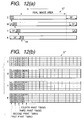
- pixel values or a pixel value group for C image data are stored at the sequential addresses in the image buffer 31', the number of which is equivalent to the number of ink-jet nozzles that are arranged in the columnar direction for a C nozzle array of the print head. Then, pixel values or pixel value groups for C image data, which are sequentially generated and which correspond to the number of C ink-jet nozzles, are stored at the addresses in the image buffer 31' that are separated by a distance that corresponds to the number of ink-jet nozzles for the image buffer 31' x (the number of nozzle arrays - 1).
- byte data 1 to 5 are stored at five sequential addresses, 1 to 5, in the image buffer 31' that correspond to the number of C ink-jet nozzles.
- data for a pixel value group for the next C image data i.e., byte data 6 to 10, which are sequentially generated, are stored at five addresses, 21 to 25, in the image buffer 31' that correspond to the number of C ink-jet nozzles and that are separated by a distance corresponding to 15 bits, which is 5 (ink-jet nozzle count) x [4 (total CMYK nozzle array count) - 1].
- the storage of data is repeated in the same manner for data Ca, Cb, Cc and Cd (not shown), each of which is five bytes long.
- Pixel values or a pixel value group for image data for M ink-jet nozzle arrays which follows array C, i.e, byte data 101 to 105, are stored at five addresses, 6 to 10, in the image buffer 31' that follows the addresses, 1 to 5, at which Ca are stored and that correspond in number to the M ink-jet nozzles.
- a pixel value group for the next M image data i.e., byte data 106 to 110 that are sequentially generated, are stored at five addresses, 26 to 30, in the image buffer 31' that correspond in number to the M ink-jet nozzles and that are separated by a distance corresponding to 15 bits, which is 5 (ink-jet nozzle count) x [4 (total CMYK nozzle array count) - 1].
- the storage of data is repeated in the same manner for data Ma, Mb, Mc and Md (not shown), each of which is five bytes.
- Pixel values or a pixel value group for Y and K image data are stored in the same manner as for C and M, and this process is repeated for data Ya, Yb, Yc and Yd (not shown) and Ka, Kb, Kc and Kd (not shown), each of which is five bytes.
- the transfer process 37 for transferring data from the image buffer 31' to the print head 33 first, data Ca, Ma, Ya and Ka, each of which is five bytes, a total of 20 bytes, are transmitted to the print head 33 simultaneously in accordance with the first printing timing. Then, data Cb, Mb, Yb and Kb, each of which is five bytes, a total of 20 bytes, are transmitted to the print head 33 simultaneously in accordance with the second printing timing. This transfer process is repeated in accordance with the third, the fourth printing timing, and each time C, M, Y and K data, each of which is five bytes, a total of 20 bytes, are transmitted simultaneously.
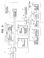
- Fig. 8 is shown an example for the second embodiment wherein in the transfer process 37 the image data are transferred to the print head 33 by using a program, and DMA is employed for their transfer to the print head 33.
- the serial printer in Fig. 8 comprises a printer controller 1 and a print engine 2.
- the printer controller 1 comprises an interface (hereinafter referred to as an "I/F") 4, for receiving print data from a host computer 3; a RAM 5, in which various data are stored; a ROM 6, in which routines for various data processes are stored; a CPU 7; an oscillator 8; a print ASIC controller 9, for transmitting head data to a print head 11 that will be described later; and an I/F 10, for transmitting to the print engine 2 print data that are developed into dot pattern data (bitmapped data) and drive signals.
- the I/F 4, the RAM 5, the ROM 6, the CU 7, the print ASIC controller 9 and the I/F 10 are interconnected by a bus 11.
- the I/F 4 receives from the host computer 3 print data consisting of, for example, image data.
- the RAM 5 is used as a data reception buffer 5A, an image output buffer 5C and a work memory (not shown).
- the data buffer 5A are temporarily stored print data consisting of image data that are received by the I/F 4 from the host computer 3.
- image buffer 5C are developed dot pattern data that are obtained by decoding tone data.
- the ROM 6 are stored various control programs to be executed by the CPU 7.
- the print ASIC controller 9 controls a head driver, and includes a register (head date register) 9a for transmitting the print data to a print head 12.
- the CPU 7 performs the imaging process 35 described in the first and the second embodiments in accordance with the main program 6a stored in the ROM 6. That is, the CPU 7 reads the print data from the data buffer 5A and stores them in the work memory in the RAM 5.
- the CPU 7 analyzes the data read from the work memory, and refers to the dot data and the graphic function in the ROM 6 to develop the data into dot pattern data. A required accessory process is performed for the obtained dot pattern data, and the resultant data are stored in the image buffer 5C. Further, the CPU 7 performs the imaging process 35 and the transfer process 37 at the same time. In other words, when an interrupt occurs at a predetermined print timing (print trigger), the CPU 7 halts the execution of the main program 6a and initiates the interrupt program 6b.
- print timing print trigger
- a set of data comprising of a plurality of bytes for C, M, Y and K color nozzles, which are used for sequential addresses, are read from the image buffer 5C, and at the same time, are transferred to the head data register 9a.
- the data are temporarily stored in the head data register 9a, and are then transmitted in series via the I/F 10 to the print head 12.
- the print engine 2 comprises the print head 12, a carriage mechanism 13 and a paper feeding mechanism 14.
- the paper feeding mechanism 14, which includes a paper feeding motor and a paper feeding roller, sequentially transfers a recording medium, such as a recording sheet, and performs sub-scanning.
- the carriage mechanism 13 includes a carriage on which the print head 12 is mounted, and a carriage motor for driving the carriage along a timing belt, and performs the main displacement of the print head 12.
- data which are temporarily stored in the head data register 9a, are transmitted in series, in synchronization with a clock signal (CK) from the oscillator 8, via the I/F 10 to a shift register 12b in the print head 12.
- the print data which are transmitted in series, are latched by a latch circuit 12c and are boosted by a level shifter (not shown), and the resultant data are transmitted to a switching circuit to control its operation.
- Fig. 9 is a flowchart showing the processing performed by the serial printer in Fig. 8 for transferring data to the print head in accordance with the program (software).
- pointers are set for four colors of C, M, Y and K (S91), and when a transfer timing (print trigger) is generated (S92), a value for four colors C, M, Y and K is set in a counter (S93).
- a transfer timing print trigger
- S92 a value for four colors C, M, Y and K is set in a counter
- S94 data for a plurality of bytes for the C, M, Y and K color nozzle arrays are transmitted to the print head 33, and during this transmission, the pointers are updated and the value held by the counter is decremented (S94).
- program control returns to S92 to wait for the next transfer timing.
- a DMA controller 7a that has two transfer circuits (channels).
- the transfer of data begins with the activation of the DMA transfer function.
- a signal (print trigger) is received at the CPU 7 in accordance with the above described print timing, the CPU 7 assigns the right of usage of the bus 11 to the DMA controller 7a.
- the DMA controller 7a transmits a set of image data for a plurality of bytes for the C, M, Y and K color nozzle arrays, which serve as sequential addresses, from the addresses in the image buffer 5C, in which the image data are stored, via the bus 11 to the head data register 9a, i.e., the DMA transfer is performed. Since the DMA transfer requires only an extremely short time, the CPU 7 can immediately initiate a subsequent process.
- the DMA controller 7a transmits a trigger signal to the oscillator 8.
- the oscillator 8 employs an oscillator to generate a clock having a frequency that corresponds to the maximum speed of the shift register 12b of the print head 12.
- the oscillator 8 is activated upon receipt of the trigger signal, and outputs a clock having bits equivalent in count to the number of nozzles for each ink-jet nozzle array 12a.
- the head data are transmitted as serial data from the head data register 9a to the shift register 12b of the print head 12. The above processing is repeated for data for eight horizontally arranged bits (one byte).
- the above described DMA transfer can be performed via the same transfer circuit (channel), and thus, if there is at least one transfer circuit channel the DMA transfer can be employed.
- a DMA controller such as the DMA controller 7a, that is built into the CPU and has only a few transfer circuits (channels) can be used to perform a DMA transfer to a print head, and the process that is performed in accordance with the program can be performed at high speed for an extended period of time.
- the invention cited in claim 9 is not limited to the color printer, but can be used for a monochrome printer having a plurality of nozzle arrays that are separated from each other.
- the raster graphics image data have been employed. That is, an example has been described where, in the imaging process, pixel values or pixel value groups for image data are generated in the raster scanning order, and are rearranged from in the raster scanning order into the order in which they are printed by the print head.
- the present invention is not limited to this example, and the second embodiment especially can be used for an example where data are transmitted as a bit-image command from the host computer.
- the present invention can be used not only for an ink-jet printer, but also for another serial printer having dot formation element arrays, such as a dot impact printer.
- the DMA controller in the CPU performs the DMA transfer of head data.
- This embodiment may be used for a printer that includes a separate DMA controller not included as part of a CPU.
- pixel values or a pixel value group for image data which are set for a specific dot formation element array of a print head at the same print timing, are stored at sequential addresses in an image buffer. Therefore, since the continuity of image data can be obtained and a set of data can be transmitted, the number of address calculations and the number of memory accesses can be reduced, and as the load imposed on the CPU during the data transfer can also be reduced, the throughout can be improved.
- the number of address calculations performed during the transfer process can be reduced, and as the time required for the process, which time is very limited, can also be reduced, the throughout can be increased.
Landscapes
- Physics & Mathematics (AREA)
- Engineering & Computer Science (AREA)
- Mathematical Physics (AREA)
- General Engineering & Computer Science (AREA)
- General Physics & Mathematics (AREA)
- Theoretical Computer Science (AREA)
- Record Information Processing For Printing (AREA)
- Dot-Matrix Printers And Others (AREA)
Applications Claiming Priority (6)
| Application Number | Priority Date | Filing Date | Title |
|---|---|---|---|
| JP58729/97 | 1997-03-13 | ||
| JP5872997 | 1997-03-13 | ||
| JP5872997 | 1997-03-13 | ||
| JP21663097 | 1997-08-11 | ||
| JP21663097A JP3533895B2 (ja) | 1997-03-13 | 1997-08-11 | シリアルプリンタ及びシリアルプリンタにおけるイメージバッファアクセス方法 |
| JP216630/97 | 1997-08-11 |
Publications (3)
| Publication Number | Publication Date |
|---|---|
| EP0871139A2 true EP0871139A2 (de) | 1998-10-14 |
| EP0871139A3 EP0871139A3 (de) | 2001-09-05 |
| EP0871139B1 EP0871139B1 (de) | 2006-10-11 |
Family
ID=26399752
Family Applications (1)
| Application Number | Title | Priority Date | Filing Date |
|---|---|---|---|
| EP98301778A Expired - Lifetime EP0871139B1 (de) | 1997-03-13 | 1998-03-11 | Seriendrucker und Bildpufferzugriffsverfahren für einen Seriendrucker |
Country Status (4)
| Country | Link |
|---|---|
| US (1) | US6009245A (de) |
| EP (1) | EP0871139B1 (de) |
| JP (1) | JP3533895B2 (de) |
| DE (1) | DE69836110T2 (de) |
Cited By (2)
| Publication number | Priority date | Publication date | Assignee | Title |
|---|---|---|---|---|
| EP0903691A3 (de) * | 1997-07-28 | 2000-06-07 | Canon Kabushiki Kaisha | Druckertreiber für einen Farbdrucker |
| EP2701376A1 (de) * | 2012-08-23 | 2014-02-26 | Kyocera Document Solutions Inc. | Bildverarbeitungsvorrichtung und Bildverarbeitungsverfahren |
Families Citing this family (11)
| Publication number | Priority date | Publication date | Assignee | Title |
|---|---|---|---|---|
| US6298652B1 (en) * | 1999-12-13 | 2001-10-09 | Exxon Mobil Chemical Patents Inc. | Method for utilizing gas reserves with low methane concentrations and high inert gas concentrations for fueling gas turbines |
| JP2002113905A (ja) * | 2000-10-06 | 2002-04-16 | Fuji Xerox Co Ltd | 画像形成装置 |
| US7336380B2 (en) | 2001-02-13 | 2008-02-26 | Heidelberger Druckmaschinen Ag | Raster generation system and method of processing raster data |
| US7679772B2 (en) * | 2003-03-24 | 2010-03-16 | Canon Kabushiki Kaisha | Printing apparatus and printing data control method effecting distributed driving of printing elements |
| US6971075B2 (en) * | 2003-07-25 | 2005-11-29 | Destiny Technology Corporation | Circuit design method to control access pointers of different memory |
| JP4556440B2 (ja) * | 2004-02-12 | 2010-10-06 | ブラザー工業株式会社 | 記録ヘッドの駆動装置及び記録装置 |
| JP2006264319A (ja) * | 2005-02-22 | 2006-10-05 | Fuji Photo Film Co Ltd | 画像データ格納方法および制御装置並びにプログラム、フレームデータ作成方法および装置並びにプログラム、データ取得方法および装置、描画方法および装置 |
| TW200642440A (en) * | 2005-02-22 | 2006-12-01 | Fuji Photo Film Co Ltd | Image data storing method and control device and program, frame data generation method and its device and program, drawing method and device |
| CN107521226B (zh) * | 2016-06-21 | 2019-03-12 | 北大方正集团有限公司 | 一种数据处理方法、装置及喷墨印刷机 |
| CN109471602B (zh) * | 2018-12-07 | 2022-09-13 | 森大(深圳)技术有限公司 | 打印数据拆分处理方法、装置及打印设备 |
| US10635955B1 (en) | 2019-05-31 | 2020-04-28 | Kyocera Document Solutions Inc. | Image forming method, apparatus, and program separating addresses for storing color tone data by shifting the relative address using an offset address |
Family Cites Families (6)
| Publication number | Priority date | Publication date | Assignee | Title |
|---|---|---|---|---|
| JPS58195358A (ja) * | 1982-05-11 | 1983-11-14 | Canon Inc | 縦横変換装置 |
| JPS58195359A (ja) * | 1982-05-11 | 1983-11-14 | Canon Inc | 縦横変換装置 |
| US4567570A (en) * | 1983-02-16 | 1986-01-28 | Exxon Research And Engineering Co. | Electronic control system for a linearly slanted print head |
| US5511151A (en) * | 1992-06-10 | 1996-04-23 | Canon Information Systems, Inc. | Method and apparatus for unwinding image data |
| JP3347527B2 (ja) * | 1994-07-01 | 2002-11-20 | キヤノン株式会社 | プリンタ及びプリント方法 |
| JPH09300735A (ja) * | 1996-05-13 | 1997-11-25 | Mitsubishi Electric Corp | 印字制御装置 |
-
1997
- 1997-08-11 JP JP21663097A patent/JP3533895B2/ja not_active Expired - Fee Related
-
1998
- 1998-03-11 DE DE69836110T patent/DE69836110T2/de not_active Expired - Lifetime
- 1998-03-11 EP EP98301778A patent/EP0871139B1/de not_active Expired - Lifetime
- 1998-03-13 US US09/041,749 patent/US6009245A/en not_active Expired - Lifetime
Cited By (3)
| Publication number | Priority date | Publication date | Assignee | Title |
|---|---|---|---|---|
| EP0903691A3 (de) * | 1997-07-28 | 2000-06-07 | Canon Kabushiki Kaisha | Druckertreiber für einen Farbdrucker |
| US6339480B1 (en) | 1997-07-28 | 2002-01-15 | Canon Kabushiki Kaisha | Print driver for a color printer |
| EP2701376A1 (de) * | 2012-08-23 | 2014-02-26 | Kyocera Document Solutions Inc. | Bildverarbeitungsvorrichtung und Bildverarbeitungsverfahren |
Also Published As
| Publication number | Publication date |
|---|---|
| DE69836110T2 (de) | 2007-05-03 |
| US6009245A (en) | 1999-12-28 |
| EP0871139B1 (de) | 2006-10-11 |
| JPH10312254A (ja) | 1998-11-24 |
| JP3533895B2 (ja) | 2004-05-31 |
| DE69836110D1 (de) | 2006-11-23 |
| EP0871139A3 (de) | 2001-09-05 |
Similar Documents
| Publication | Publication Date | Title |
|---|---|---|
| EP1013423B1 (de) | Tintenstrahldruckkopf und damit versehene Druckvorrichtung | |
| US6009245A (en) | Serial printer, and image buffer access method for serial printer | |
| EP0551095B1 (de) | Serieller Rasterbilddrucker und Verfahren zu dessen Betrieb | |
| EP0782095B1 (de) | Tintenstrahldrucker und Steuerungsverfahren | |
| EP0690410B1 (de) | Drucker mit rollierendem Drucker-Pufferspeicher, und Druckverfahren | |
| EP0646889B1 (de) | Aufzeichnungsgerät | |
| US20050099440A1 (en) | Print control device and print control method | |
| US6712450B2 (en) | Ink jet printer | |
| JP2011076156A (ja) | 画像処理装置および画像処理方法 | |
| US5740332A (en) | Image forming device | |
| US5768484A (en) | Printing apparatus and control method therefor | |
| US5672016A (en) | Method for controlling color image data | |
| JP6844459B2 (ja) | 画像処理システム、画像処理方法および画像処理装置、ならびに、画像形成システム | |
| US7377607B2 (en) | Liquid ejecting apparatus and method of transferring image data | |
| JP2007276353A (ja) | インクジェット記録装置、インクジェット記録装置の記録制御方法、プログラム及び記憶媒体 | |
| JP2003103846A (ja) | インクジェットプリンタ | |
| JP4544142B2 (ja) | 画像処理装置、プリンタドライバ、印刷システム、プログラム | |
| JP3885247B2 (ja) | 画像記録装置 | |
| JP2007015248A (ja) | 記録装置 | |
| JP4605271B2 (ja) | 画像出力装置 | |
| JP2000141619A (ja) | 記録方法及び装置 | |
| JP2001187476A (ja) | プリンタ及びそのイメージデータの転送方法 | |
| HK1011778B (en) | Recording apparatus | |
| JP2003251794A (ja) | プリンタ、及び、その制御方法 | |
| JP2002059589A (ja) | プリンタ装置、印刷方法、並びにコンピュータが読出し可能なプログラムを格納した記憶媒体 |
Legal Events
| Date | Code | Title | Description |
|---|---|---|---|
| PUAI | Public reference made under article 153(3) epc to a published international application that has entered the european phase |
Free format text: ORIGINAL CODE: 0009012 |
|
| AK | Designated contracting states |
Kind code of ref document: A2 Designated state(s): AT BE CH DE DK ES FI FR GB GR IE IT LI LU MC NL PT SE |
|
| AX | Request for extension of the european patent |
Free format text: AL;LT;LV;MK;RO;SI |
|
| PUAL | Search report despatched |
Free format text: ORIGINAL CODE: 0009013 |
|
| AK | Designated contracting states |
Kind code of ref document: A3 Designated state(s): AT BE CH DE DK ES FI FR GB GR IE IT LI LU MC NL PT SE |
|
| AX | Request for extension of the european patent |
Free format text: AL;LT;LV;MK;RO;SI |
|
| 17P | Request for examination filed |
Effective date: 20011210 |
|
| AKX | Designation fees paid |
Free format text: DE FR GB |
|
| 17Q | First examination report despatched |
Effective date: 20040419 |
|
| GRAP | Despatch of communication of intention to grant a patent |
Free format text: ORIGINAL CODE: EPIDOSNIGR1 |
|
| GRAS | Grant fee paid |
Free format text: ORIGINAL CODE: EPIDOSNIGR3 |
|
| GRAA | (expected) grant |
Free format text: ORIGINAL CODE: 0009210 |
|
| AK | Designated contracting states |
Kind code of ref document: B1 Designated state(s): DE FR GB |
|
| REG | Reference to a national code |
Ref country code: GB Ref legal event code: FG4D |
|
| REF | Corresponds to: |
Ref document number: 69836110 Country of ref document: DE Date of ref document: 20061123 Kind code of ref document: P |
|
| ET | Fr: translation filed | ||
| PLBE | No opposition filed within time limit |
Free format text: ORIGINAL CODE: 0009261 |
|
| STAA | Information on the status of an ep patent application or granted ep patent |
Free format text: STATUS: NO OPPOSITION FILED WITHIN TIME LIMIT |
|
| 26N | No opposition filed |
Effective date: 20070712 |
|
| REG | Reference to a national code |
Ref country code: FR Ref legal event code: PLFP Year of fee payment: 19 |
|
| PGFP | Annual fee paid to national office [announced via postgrant information from national office to epo] |
Ref country code: DE Payment date: 20160308 Year of fee payment: 19 |
|
| PGFP | Annual fee paid to national office [announced via postgrant information from national office to epo] |
Ref country code: GB Payment date: 20160309 Year of fee payment: 19 Ref country code: FR Payment date: 20160208 Year of fee payment: 19 |
|
| REG | Reference to a national code |
Ref country code: DE Ref legal event code: R119 Ref document number: 69836110 Country of ref document: DE |
|
| GBPC | Gb: european patent ceased through non-payment of renewal fee |
Effective date: 20170311 |
|
| REG | Reference to a national code |
Ref country code: FR Ref legal event code: ST Effective date: 20171130 |
|
| PG25 | Lapsed in a contracting state [announced via postgrant information from national office to epo] |
Ref country code: DE Free format text: LAPSE BECAUSE OF NON-PAYMENT OF DUE FEES Effective date: 20171003 Ref country code: FR Free format text: LAPSE BECAUSE OF NON-PAYMENT OF DUE FEES Effective date: 20170331 |
|
| PG25 | Lapsed in a contracting state [announced via postgrant information from national office to epo] |
Ref country code: GB Free format text: LAPSE BECAUSE OF NON-PAYMENT OF DUE FEES Effective date: 20170311 |