EP0871231A2 - Elément magnéto-résistif - Google Patents
Elément magnéto-résistif Download PDFInfo
- Publication number
- EP0871231A2 EP0871231A2 EP98302429A EP98302429A EP0871231A2 EP 0871231 A2 EP0871231 A2 EP 0871231A2 EP 98302429 A EP98302429 A EP 98302429A EP 98302429 A EP98302429 A EP 98302429A EP 0871231 A2 EP0871231 A2 EP 0871231A2
- Authority
- EP
- European Patent Office
- Prior art keywords
- layer
- magnetization
- ferromagnetic layer
- magnetic
- pinned
- Prior art date
- Legal status (The legal status is an assumption and is not a legal conclusion. Google has not performed a legal analysis and makes no representation as to the accuracy of the status listed.)
- Withdrawn
Links
Images




Classifications
-
- B—PERFORMING OPERATIONS; TRANSPORTING
- B82—NANOTECHNOLOGY
- B82Y—SPECIFIC USES OR APPLICATIONS OF NANOSTRUCTURES; MEASUREMENT OR ANALYSIS OF NANOSTRUCTURES; MANUFACTURE OR TREATMENT OF NANOSTRUCTURES
- B82Y25/00—Nanomagnetism, e.g. magnetoimpedance, anisotropic magnetoresistance, giant magnetoresistance or tunneling magnetoresistance
-
- H—ELECTRICITY
- H10—SEMICONDUCTOR DEVICES; ELECTRIC SOLID-STATE DEVICES NOT OTHERWISE PROVIDED FOR
- H10N—ELECTRIC SOLID-STATE DEVICES NOT OTHERWISE PROVIDED FOR
- H10N50/00—Galvanomagnetic devices
- H10N50/10—Magnetoresistive devices
-
- G—PHYSICS
- G01—MEASURING; TESTING
- G01R—MEASURING ELECTRIC VARIABLES; MEASURING MAGNETIC VARIABLES
- G01R33/00—Arrangements or instruments for measuring magnetic variables
- G01R33/02—Measuring direction or magnitude of magnetic fields or magnetic flux
- G01R33/06—Measuring direction or magnitude of magnetic fields or magnetic flux using galvano-magnetic devices
- G01R33/09—Magnetoresistive devices
- G01R33/093—Magnetoresistive devices using multilayer structures, e.g. giant magnetoresistance sensors
-
- G—PHYSICS
- G11—INFORMATION STORAGE
- G11B—INFORMATION STORAGE BASED ON RELATIVE MOVEMENT BETWEEN RECORD CARRIER AND TRANSDUCER
- G11B5/00—Recording by magnetisation or demagnetisation of a record carrier; Reproducing by magnetic means; Record carriers therefor
- G11B5/127—Structure or manufacture of heads, e.g. inductive
- G11B5/33—Structure or manufacture of flux-sensitive heads, i.e. for reproduction only; Combination of such heads with means for recording or erasing only
- G11B5/39—Structure or manufacture of flux-sensitive heads, i.e. for reproduction only; Combination of such heads with means for recording or erasing only using magneto-resistive devices or effects
- G11B5/3903—Structure or manufacture of flux-sensitive heads, i.e. for reproduction only; Combination of such heads with means for recording or erasing only using magneto-resistive devices or effects using magnetic thin film layers or their effects, the films being part of integrated structures
- G11B5/3906—Details related to the use of magnetic thin film layers or to their effects
- G11B5/3929—Disposition of magnetic thin films not used for directly coupling magnetic flux from the track to the MR film or for shielding
- G11B5/3932—Magnetic biasing films
-
- H—ELECTRICITY
- H01—ELECTRIC ELEMENTS
- H01F—MAGNETS; INDUCTANCES; TRANSFORMERS; SELECTION OF MATERIALS FOR THEIR MAGNETIC PROPERTIES
- H01F10/00—Thin magnetic films, e.g. of one-domain structure
- H01F10/32—Spin-exchange-coupled multilayers, e.g. nanostructured superlattices
- H01F10/324—Exchange coupling of magnetic film pairs via a very thin non-magnetic spacer, e.g. by exchange with conduction electrons of the spacer
- H01F10/3268—Exchange coupling of magnetic film pairs via a very thin non-magnetic spacer, e.g. by exchange with conduction electrons of the spacer the exchange coupling being asymmetric, e.g. by use of additional pinning, by using antiferromagnetic or ferromagnetic coupling interface, i.e. so-called spin-valve [SV] structure, e.g. NiFe/Cu/NiFe/FeMn
-
- H—ELECTRICITY
- H10—SEMICONDUCTOR DEVICES; ELECTRIC SOLID-STATE DEVICES NOT OTHERWISE PROVIDED FOR
- H10N—ELECTRIC SOLID-STATE DEVICES NOT OTHERWISE PROVIDED FOR
- H10N50/00—Galvanomagnetic devices
- H10N50/80—Constructional details
- H10N50/85—Materials of the active region
Definitions
- the present invention relates to a magnetoresistive element constituting a magnetoresistive element used for magnetic heads, positioning sensors, rotation sensors and the like.
- MR head Conventional magnetoresistive reading heads (MR head) comprise AMR (Anisotropic Magnetoresistance) heads utilizing an anisotropic megnetoresistance phenomenon and GMR (Giant Magnetoresistance) heads utilizing a spin depending scattering phenomenon of conductive electrons, a spin-valve head that exhibit a high magnetoresistive effect at low external magnetic field being disclosed in the specification of US patent publication No. 5,159,513 as one example of GMR heads.
- Fig. 9 is one example of the conventional spin-valve structure, which is constructed by laminating a free ferromagnetic layer 1 , a nonmagnetic intermediate layer 2 , a pinned ferromagnetic layer 3 and an antiferromagnetic layer 4 on a substrate, providing two magnet layers 5 , 5 comprising Co-Pt and the like at both sides of this laminated member so as to insert the laminated member between the magnet layers, on which two electrode layers 6 , 6 are provided.
- a relatively large bias magnetic field is needed to fix the direction of magnetization of the pinned ferromagnetic layer 3 along the z-direction in Fig. 9, a larger vias magnetic field being preferable.
- a vias magnetic field of at least 100 Oe is required in order to overcome an antimagnetic field along the z-direction in Fig. 9 thereby preventing the direction of magnetization from being fluctuated due to a magnetic flux from a magnetic medium.
- An exchange anisotropic magnetic field generated by providing a pinned ferromagnetic layer 3 in contact with an exchange coupling layer 4 is utilized in the conventional structure shown in Fig. 9 to obtain this vias magnetic field.
- magnetization should be made to direct toward the track direction as a single magnetic domain by impressing a vertical vias parallel to the film face (X-direction in Fig. 9: the track direction) on the free ferromagnetic layer 1 from the magnet layers 5 , 5 , along with allowing the direction of magnetization of the pinned ferromagnetic layer 3 to direct toward the Z-direction in Fig. 9 as a single magnetic domain by impressing a vias along the Z-direction in Fig. 9, that is, a direction perpendicular to magnetization of the free ferromagnetic layer 1 .
- the object of impressing a vertical vias is to suppress Barkhausen noise arising from a lot of magnetic domains formed by the free ferromagnetic layer 1 or, in other words, to make resistance against the magnetic flux from a magnetic medium to change smoothly with low noise levels.
- the direction of magnetization of the pinned ferromagnetic layer 3 should not be changed by the magnetic flux (along the Z-direction in Fig. 9) from the magnetic medium. Rather, a linear response could be obtained by allowing the direction of the free ferromagnetic layer 1 to change in a range of 90 ⁇ ⁇ ° relative to the direction of magnetization.
- a magnetoresistive head having a good linear response in which Barkhausen noise is suppressed can be realized by taking advantage of a vias in the pinned ferromagnetic layer at the spin valve head, and the exchange anisotropic magnetic field generated in the vertical vias of the free ferromagnetic layer at a contact interface with the antiferromagnetic layer.
- the exchange anisotropic magnetic field is a phenomenon arising from an exchange interaction between magnetic moments of the ferromagnetic layer and exchange coupling layer at a contact face between the two layers.
- corrosion resistance of FeMn layer is so poor that corrosion is progressed during the manufacturing process of magnetic heads or operation of magnetic heads, thereby largely deteriorating the exchange anisotropic magnetic field.
- the exchange anisotropic magnetic field created by the FeMn layer is so sensitive to temperature changes that the exchange anisotropic magnetic field is approximately linearly reduced against temperature until it has ben quenched at a temperature of about 150 °C (a blocking temperature: Tb). Accordingly, there remains a problem that a stable exchange anisotropic magnetic field is hardly obtainable.
- a pinned ferromagnetic layer is formed by pinning rotation of magnetization of the ferromagnetic layer by disposing a coercive force increasing layer of ⁇ -Fe 2 O 3 to one of the two ferromagnetic layers laminated via non-magnetic layers while a free magnetic layer is formed by allowing magnetization of the other ferromagnetic layer to be freely rotated, thereby arising a resistance change by making the free ferromagnetic layer to rotate by the external magnetic field.
- the magnetoresistive element having the structure described above Since the blocking temperature of ⁇ -Fe 2 O 3 is far more higher than that of FeMn, the magnetoresistive element having the structure described above has an advantage that its magnetic properties are hardly changed by temperature variations, characterized by having no problem in corrosion resistance because ⁇ -Fe 2 O 3 itself is an oxide.
- the orientation of magnetization in the free ferromagnetic layer 1 of the free ferromagnetic layer 1 and pinned ferromagnetic layer 3 provided by inserting a non-magnetic layer 2 therebetween should be freely rotated by sensitively responding to the external magnetic field in the magnetoresistive element with a spin valve structure using FeMn, or in the magnetoresistive element provided with a coercive force increasing layer of ⁇ -Fe 2 O 3 , it is preferable that the coercive force is small. On the contrary, the orientation of the pinned ferromagnetic layer 3 should not be made to move by responding to the external magnetic field.
- the coercive force of the free ferromagnetic layer 1 is increased higher than the inherent level of the material due to the effect of the magnetic field created by the pinned ferromagnetic layer 3 , hindering free rotation of magnetization of the free ferromagnetic layer 1 , so that characteristics of R - H curves as a magnetoresistive element may be possibly deteriorated.
- the object of the present invention which is carried out by taking the above situations into account, is to provide a magnetoresistive element being made easy to reverse magnetization as a result of low coercive force of the free ferromagnetic layer by providing with an auxiliary magnetization reversing layer and exhibiting a magnetoresistive effect sensitively responding to the external magnetic field, wherein the magnetoresistive effect can be prevented from being decreased by depressing the electric current that tends to be branched into the auxiliary magnetization reversing layer by providing the auxiliary magnetization reversing layer with a material of high resistivity.
- the present invention is characterized by being provided with at least one pinned ferromagnetic layer in which inversion of magnetization is pinned, at least one free ferromagnetic layer in which magnetization is freely rotated against the external magnetic field, and an auxiliary magnetization reversing layer assisting inversion of magnetization of the ferromagnetic layer by being disposed in adjoining relation or in closely spaced relation to the free ferromagnetic layer and having an auxiliary magnetization reversing layer with soft magnetic characteristics.
- the auxiliary magnetization reversing layer mainly comprises a fine crystalline phase principally composed of bcc Fe structure and an amorphous phase containing an element M comprising one or a plurality of elements selected from Ti, Zr, Hf, V, Nb, Ta, W and rare earth elements, and O (oxygen).
- the auxiliary magnetization reversing layer mainly comprises a fine crystalline phase principally composed of bcc Fe structure and a crystalline phase containing carbide and nitride of an element M' comprising one or a plurality of elements selected from Ti, Zr, Hf, V, Nb, Ta, W and rare earth elements.
- the pinned ferromagnetic layer is provided in adjoining relation to an exchange coupling layer so that inversion of magnetization of pinned ferromagnetic layer is pinned in response to the magnetic exchange coupling due to said exchange coupling layer.
- the exchange coupling layer may be mainly composed of ⁇ -Fe 2 O 3 while the exchange coupling layer is mainly composed of a X-Mn alloy, wherein X in the composition formula X-Mn denotes one or a plurality of elements selected from platinum group elements.
- the thickness of the auxiliary magnetization reversing layer is in the range of 50 to 300 ⁇ and the specific resistivity of the auxiliary magnetization reversing layer is in the range of 200 to 2 ⁇ 10 5 ⁇ cm.
- Fig. 1 is a cross section showing the 1st aspect of the magnetoresistive multilayer film according to the present invention.
- Fig. 2 is a cross section showing the 2nd aspect of the magnetoresistive multilayer film according to the present invention.
- Fig. 3 is a cross section showing the 3rd aspect of the magnetoresistive multilayer film according to the present invention.
- Fig. 4 is a cross section showing the 4th aspect of the magnetoresistive multilayer film according to the present invention.
- Fig. 5 is a graph indicating a M-H curve of a sample of the soft magnetic layer (a layer of Fe 60 Hf 10 O 30 ) provided on the Si substrate covered with a Al 2 O 3 layer.
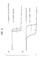
- Fig. 6 shows a R-H curve of the free ferromagnetic layer of the magnetoresistive multilayer film having a laminated construction of Si substrate / Al 2 O 3 layer / ⁇ -Fe 2 O 3 layer / NiFe layer / Cu layer / NiFe layer / Fe 60 Hf 10 O 30 layer, and a R-H curve of the free ferromagnetic layer of the magnetoresistive multilayer film having a construction in which Fe 60 Hf 10 O 30 layer is omitted in the foregoing laminated structure.
- Fig. 7 shows a R-H curve of the free ferromagnetic layer of the magnetoresistive multilayer film having a laminated construction of Si substrate / Al 2 O 3 layer / ⁇ -Fe 2 O 3 / NiFe layer / Co layer / Cu layer / Co layer / NiFe layer / Fe 60 Hf 10 O 30 and a R-H curve of the free ferromagnetic layer of the magnetoresistive multilayer film having a construction in which the Fe 60 Hf 10 O 30 layer is omitted in the foregoing laminated structure.
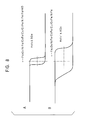
- Fig. 8 shows a R-H curve of the free ferromagnetic layer of the magnetoresistive multilayer film having a laminated construction of Si substrate / Al 2 O 3 layer / ⁇ -Fe 2 O 3 / NiFe layer / CoFe layer / Cu layer / CoFe layer / NiFe layer / Fe 60 Hf 10 O 30 layer, and R-H curve of the free ferromagnetic layer of the magnetoresistive multilayer film having a construction in which Fe 60 Hf 10 O 30 layer is omitted in the foregoing laminated structure.
- Fig. 9 is a cross section of the 1st aspect of the conventional magnetoresistive sensor.
- Fig. 1 is an aspect of a magnetoresistive multilayer film provided on the magnetoresistive element according to the present invention, wherein the magnetoresistive multilayer film A of this configuration is mainly composed of a substrate 10 of a non-magnetic member, and a pinning thin film layer 11 , a pinned ferromagnetic layer 12 , a non-magnetic layer 13 , a free ferromagnetic layer 14 , an auxiliary magnetization reversing layer 15 and a protective layer 16 each being laminated thereon.
- the substrate 10 is composed of a non-magnetic material represented by a glass, Si, Al 2 O 3 , TiC, SiC and a sintered body of Al 2 O 3 and TiC.
- a cover layer and a buffer layer may be appropriately provided on the substrate 10 for the purpose of eliminating roughness of the substrate surface or to make crystalline matching of the layer laminated thereon comfortable.
- An exchange coupling layer 11 is provided in order to enhance coercive force of the pinned ferromagnetic layer 12 by allowing a magnetic exchange coupling force to effect on the pinned ferromagnetic layer 12 formed thereon. It is preferable that this exchange coupling layer 11 is composed of an antiferromagnetic material, especially an oxide antiferromagnetic material, an example of which being ⁇ -Fe 2 O 3 . A hard magnetic material may be also used for this exchange coupling layer 11 , an example of it being Co-Pt alloy and the like.
- a magnetoresistive multilayer film being excellent in linear response in addition to being robust in temperature changes and securely suppressing Barkhausen noise can be provided if the exchange coupling layer 11 is composed of ⁇ -Fe 2 O 3 because the Molin point of ⁇ -Fe 2 O 3 itself is high.
- the exchange coupling layer 11 can be also constructed with X-Mn alloy films (wherein X denotes one or a plurality of platinum group elements such as Pt, Pd, Ir, Ru and Rh).
- Both of the pinned ferromagnetic layer 12 and free ferromagnetic layer 14 comprise ferromagnetic thin films, examples of them being NiFe alloy, NiCo alloy and NiFeCo alloy.
- the free ferromagnetic layer 14 and pinned ferromagnetic layer 12 can be composed of a NiFe alloy layers, respectively, or the free ferromagnetic layer 14 may be constructed of a laminated structure of NiFe alloy layers or a laminated structure of CoFe alloy layers and NiFe alloy layers.
- the layer is preferably made of a magnetoresistive multilayer film B in which a metallic layer 17 such as thin Co layer or CoFe (Co 90 Fe 10 ) alloy is disposed to the non-magnetic layer 13 as shown in Fig. 2.
- a metallic layer 17 such as thin Co layer or CoFe (Co 90 Fe 10 ) alloy is disposed to the non-magnetic layer 13 as shown in Fig. 2.
- Co may be predominantly contained in the non-magnetic layer 13 side of the ferromagnetic layer 14 to form an alloy, thereby forming a concentration gradient gradually decreasing Co concentration along the direction toward the auxiliary magnetization reversing layer 15 , instead of especially providing a Co layer.
- the non-magnetic layer 13 comprises a non-magnetic material represented by Cu, Cr, Au and Ag with a thickness of 20 to 40 ⁇ .
- the thickness of the non-magnetic layer 13 is less than 20 ⁇ , the pinned ferromagnetic layer 12 becomes ready to be magnetically coupled with the free ferromagnetic layer 14 .
- a thickness of more than 40 ⁇ of the non-magnetic layer 13 is not preferable, on the other hand, because the effectiveness of conductive electrons that pass through the interface between the non-magnetic layer 13 and ferromagnetic layers 12 and 14 and arise magnetoresistive effect is decreased, or the magnetoresistive effect is diminished due to electric current branching effect.
- the auxiliary magnetization reversing layer 15 comprises a soft magnetic material with small coercive force, large saturation magnetization, large magnetic permeability and large resistivity with a preferable thickness of 100 to 300 ⁇ , examples of them being those having the following composition.
- the preferable auxiliary magnetization reversing layer to be used in the present invention mainly composed of a fine crystalline phase principally comprising bcc Fe structure and an amorphous phase containing an element M comprising one or a plurality of elements of Ti, Zr, Hf, V, Nb, Ta, W and rare earth elements, and O (oxygen).
- the auxiliary magnetization reversing layer also mainly comprises a fine crystalline phase principally composed of bcc Fe structure and a crystalline phase containing carbides and nitride of an element M comprising one or a plurality of elements selected from Ti, Zr, Hf, V, Nb, Ta, W and rare earth elements.
- auxiliary magnetization reversing layer 15 examples of the composition of these auxiliary magnetization reversing layer 15 are as follows.
- the soft magnetic alloys with this composition can be also used for the object of the present invention because they exhibit a high resistivity of the order of 400 to 1000 ⁇ cm as shown in USP 5,573,863 disclosed by the inventors of the present invention.
- the soft magnetic alloys with this composition can be used for the object of the present invention because they exhibit a high resistivity of the order of 400 to 2.0 ⁇ 10 5 u ⁇ cm as shown in USP 5,573,863 disclosed by the inventors of the present invention.
- composition formula is represented by T 100 - a' - b' - c' - d' M' b' -Z c' -Q d' , wherein T represents any one or both of Fe and Co, X represents any one or both of Si and Al, M' represents at least one element selected from a group of Ti, Zr, Hf, V, Nb, Ta, Mo and W, Z represents any one or both of C and N, and Q represents at least one element selected from a group of Cr, Re, Ru, Rh, Ni, Pd, Pt and Au.
- composition ratio (atomic 5): 0 ⁇ a' ⁇ 25, 1 ⁇ b' ⁇ 7, and 0.5 ⁇ c' ⁇ 10.
- the soft magnetic alloys with this composition can be used for the object of the present invention because they exhibit a high saturation magnetization density of more than 1T.
- composition formula is represented by T 100 - e' - f' - b' - c' - d' Al f' M' b' -Z c' -Q d' , wherein T represents any one or both of Fe and Co, M' represents at least one element selected from a group of Ti, Zr, Hf, V, Nb, Ta, Mo and W, Z represents any one or both of C and N, and Q represents at least one element selected from a group of Cr, Re, Ru, Rh, Ni, Pd, Pt and Au.
- composition ratio 8 ⁇ e' ⁇ 15, 0.5 ⁇ f' ⁇ 10, 1 ⁇ b' ⁇ 7, 0.5 ⁇ c' ⁇ 10 and 0 ⁇ d' ⁇ 10.
- the soft magnetic alloys with this composition can be used for the object of the present invention because they exhibit a high saturation magnetization density of more than 1T.
- composition formula is represented by (Co 1- g T g ) x' M y Q z X w Y s , wherein T represents one or a plurality of elements selected from a group of Fe, Ni, Pd, Mn and Al, M represents at least one element selected from a group of Ti, Zr, Hf, Nb, Ta, M and Y, and one or a plurality of elements selected from rare earth elements, Q represents one or a plurality of elements selected from 0, N and B, X represents one or both of Si and Cr, and Y represents one or both of Au and Ag.
- g satisfies the relation of 0.05 ⁇ g ⁇ 0.5 while y, z and w satisfy the relations of 3 ⁇ y ⁇ 30, 7 ⁇ z ⁇ 40, 0 ⁇ w ⁇ 20 and 0 ⁇ s ⁇ 20, respectively in atomic %, with a balance of inevitable impurities.
- the protective layer 16 is provided for protecting the auxiliary magnetization reversing layer 15 , the former layer can be omitted.
- An insulating overcoat layer may be also provided on this protective layer 16 . It is preferable that the overcoat layer provided is composed of an insulating material such as Al 2 O 3 and quartz.
- the orientation of magnetization in the pinned ferromagnetic layer 12 is pinned and the orientation of magnetization in the ferromagnetic layer 14 is made free in the area corresponding to the track width, so that a coercive force difference between the ferromagnetic layers 12 and 14 is created, thereby arising a giant magnetoresistive effect.
- the free ferromagnetic layer 14 can be coupled with the auxiliary magnetization reversing layer 15 , thereby making it possible to reduce coercive force of the free ferromagnetic layer 14 .
- the auxiliary magnetization reversing layer 15 is able to sensitively respond to the external magnetic field owing to its small coercive force besides magnetization of the free ferromagnetic layer 14 making a contact with the auxiliary magnetization reversing layer 15 is readily rotated since its saturation magnetization is large.
- the magnetoresistive effect can be displayed with a good lineality. Since the auxiliary magnetization reversing layer 15 itself has a high specific resistivity, branching electric current being liable to flow through the auxiliary magnetization reversing layer 15 can be reduced, consequently increasing the proportion of current that flow through the interface between the non-magnetic layer 13 and ferromagnetic layers 12 and 14 to lower the reduced proportion of the magnetoresistive effect.
- heat resistance of the layer can be improved by providing a metallic layer 17 comprising Co or CoFe as shown in Fig. 2.
- the construction shown in Fig. 2 is preferable because the structure in which Co makes a contact with the non-magnetic layer exhibits a large magnetoresistive effect in the mechanism for generating magnetoresistive effect in which a non-magnetic layer of Cu is inserted into the ferromagnetic layers.
- the auxiliary magnetization reversing layer 15 provided on the free ferromagnetic layer 14 is effective because the former suppresses increase of the coercive force in the free ferromagnetic layer 14 . Accordingly, the construction shown in Fig. 2 makes it possible to obtain a magnetoresistive multilayer film having a good heat resistance and large magnetoresistive effect besides allowing resistivity to change sensitively responding to the external magnetic field.
- the exchange coupling layer 11 in the structure shown in Fig. 1 may be composed of ⁇ -Fe 2 O 3 , an oxide by itself, having a superior corrosion resistance to FeMn that is used in the conventional spin valve structure besides being characterized by its toughness to temperature variations due to its high Neel temperature.
- the resistance of the spin valve structure portion comprising a pinned ferromagnetic layer, non-magnetic layer and free magnetic layer be R sv
- the electric current flowing therethrough be i sv
- the resistance of a auxiliary magnetization reversing layer be R OL and the electric current flowing therethrough be i OL .
- i OL 's can be calculated as 0.0089 i, 0.0177 i, 0.0348 i and 0.0514 i when the layer film thickness of the auxiliary magnetization reversing layers are 50 ⁇ , 100 ⁇ , 200 ⁇ and 300 ⁇ , respectively.
- a magnetoresistive multilayer film C is formed by laminating a pinned ferromagnetic layer 32 , a non-magnetic layer 33 , a free ferromagnetic layer 34 , an auxiliary magnetization reversing layer 35 and a protective layer 36 in this order on a pinning thin film layer formed on a substrate constructing a magnetic head illustrated in the drawing, wherein two electrode layers 39 , 39 inserting the magnetoresistive multilayer film C therebetween with a space corresponding the track width TW, and two magnetic layers 40 , 40 that serve for allowing magnetization of the free ferromagnetic layer to be a single magnetic domain along X direction (the direction denoted by an arrow a in Fig. 3) are provided at both sides of the magnetoresistive multilayer film C .
- the directions of magnetization of free ferromagnetic layer 34 and magnetization of the pinned ferromagnetic layer 32 can be orthogonally aligned with each other with an angle of approximately 90° by allowing the former to direct along the direction of the arrow a in Fig. 3 and the latter to direct along the Z-direction.
- the magnetoresistive multilayer film C with the construction shown in Fig. 3 is produced by the steps comprising: placing a non-magnetic ceramic substrate made of, for example, Al 2 O 3 - TiC (Altic) in the chamber of a high frequency magnetron sputtering apparatus or an ion beam sputtering apparatus; replacing the atmosphere in the chamber with an inert gas such as Ar; and forming the layers in the required order.
- Targets required in forming the layers are, for example, ⁇ -Fe 2 O 3 target, Ni-Fe target and Cu target.
- the process for producing the magnetoresistive multilayer film A in Fig. 3 comprises: forming a pinning thin film layer 31 comprising ⁇ -Fe 2 O 3 by sputtering on a substrate while impressing a magnetic field along the Z direction in Fig. 1 in an reduced pressure of Ar of 3 mTorr or less; forming two ferromagnetic layers 32 and 34 with a non magnetic layer 33 inserted therebetween; and laminating an auxiliary magnetization reversing layer 35 and a protective layer 36 in this order. Then, the laminated layers are processed to form a magnetoresistive multilayer film C by removing the layers except the portion corresponding to the track width by a photolithographic process and ion milling. After forming the magnetoresistive multilayer film C, two magnetic layers 40 and 40 , and two electrode layers 39 and 39 are formed so that the laminated member is inserted between the layers.
- the direction of magnetization of the pinned ferromagnetic layer 32 is pinned to fix the direction of magnetization by applying a magnetic field perpendicular to the drawing paper in Fig. 3 to magnetize the pinning thin film layer 31 .
- a magnetoresistive sensor with a construction shown in Fig. 3 can be obtained by the foregoing treatment, wherein the direction of magnetization of the pinned ferromagnetic layer 32 and the direction of magnetization of the free ferromagnetic layer 34 are orthogonally aligned with each other with an angle of 90°.
- magnetization as described above is not necessary when the pinning thin film layer 31 is produced using ferromagnetic materials such as Fe-Mn, Pt-Mn and Ir-Mn, instead, the direction of magnetization of the pinned ferromagnetic layer 32 is pinned by an exchange coupling.
- the auxiliary magnetization reversing layer 15 in the magnetoresistive multilayer film A in Fig. 1 may be provided on the substrate 10 , followed by providing a free ferromagnetic layer 14 thereon in addition to providing a pinned ferromagnetic layer 12 via a non-magnetic layer 13 in the present invention.
- An underlying layer may be also provided between the substrate 10 and auxiliary magnetization reversing layer 15 , if necessary, to align the crystal orientation of the auxiliary magnetization reversing layer 15 .
- Fig. 5A and 5B show M-H curves when a soft magnetic film with a composition of Fe 60 Hf 10 O 30 is used for the auxiliary magnetization reversing layer with a construction shown in Fig. 1.
- This auxiliary magnetization reversing layer is formed on a substrate of Si covered with a protective layer of Al 2 O 3 with a thickness of 300 ⁇ .
- Fig. 5A and 5B correspond to M-H curves along the hard axis of magnetization and easy axis of magnetization, respectively.
- the soft magnetic film of this composition exhibits an excellent M-H curve as a soft magnetic film.
- Fig. 6A shows a R-H curve of the free ferromagnetic layer having a laminated construction of ⁇ -Fe 2 O 3 (coercive force increasing layer and pinning thiln film layer, thickness 1000 ⁇ ) / NiFe layer (pinned ferromagnetic layer, thickness 58 ⁇ ) / Cu layer (non-magnetic layer, thickness 22 ⁇ ) / NiFe layer (free ferromagnetic layer, thickness 87 ⁇ ) / Fe 60 Hf 10 O 30 (auxiliary magnetization reversing layer, thickness 300 ⁇ ) on a substrate of Si substrate / Al 2 O 3 layer
- Fig. 6B shows a R-H curve of the free ferromagnetic layer having a construction in which the auxiliary magnetization reversing layer is omitted in the foregoing laminated structure.
- Fig. 7A shows a R-H curve of the free ferromagnetic layer having a laminated construction of ⁇ -Fe 2 O 3 (1000 ⁇ ) / NiFe layer (48 ⁇ ) / Co layer (10 ⁇ ) / Cu layer (22 ⁇ ) / Co layer (10 ⁇ ) / NiFe layer (77 ⁇ ) / Fe 60 Hf 10 O 30 (300 ⁇ ) on a substrate of Si substrate / Al 2 O 3 layer
- Fig. 7B shows a R-H curve of the free ferromagnetic layer having a construction in which the auxiliary magnetization reversing layer is omitted in the foregoing laminated structure.
- Hcf in the figure denotes the coercive force of the free ferromagnetic layer.
- Fig. 8A shows a R-H curve of the free ferromagnetic layer having a laminated construction of ⁇ -Fe 2 O 3 (1000 ⁇ ) / NiFe layer (48 ⁇ ) / CoFe layer (10 ⁇ ) / Cu layer (22 ⁇ ) / CoFe layer (10 ⁇ ) / NiFe layer (77 ⁇ ) / Fe 60 Hf 10 O 30 (300 ⁇ ) on a substrate of Si substrate / Al 2 O 3 layer
- Fig. 8B shows a R-H curve of the free ferromagnetic layer having a construction in which the auxiliary magnetization reversing layer is omitted in the foregoing laminated structure.
- Hcf in the figure also denotes the coercive force of the free ferromagnetic layer as in Fig. 6.
Landscapes
- Engineering & Computer Science (AREA)
- Physics & Mathematics (AREA)
- Chemical & Material Sciences (AREA)
- Crystallography & Structural Chemistry (AREA)
- General Physics & Mathematics (AREA)
- Condensed Matter Physics & Semiconductors (AREA)
- Power Engineering (AREA)
- Nanotechnology (AREA)
- Manufacturing & Machinery (AREA)
- Hall/Mr Elements (AREA)
- Thin Magnetic Films (AREA)
- Measuring Magnetic Variables (AREA)
- Magnetic Heads (AREA)
Applications Claiming Priority (2)
| Application Number | Priority Date | Filing Date | Title |
|---|---|---|---|
| JP09256597A JP3198265B2 (ja) | 1997-04-10 | 1997-04-10 | 磁気抵抗効果素子 |
| JP92565/97 | 1997-04-10 |
Publications (2)
| Publication Number | Publication Date |
|---|---|
| EP0871231A2 true EP0871231A2 (fr) | 1998-10-14 |
| EP0871231A3 EP0871231A3 (fr) | 1999-05-26 |
Family
ID=14057955
Family Applications (1)
| Application Number | Title | Priority Date | Filing Date |
|---|---|---|---|
| EP98302429A Withdrawn EP0871231A3 (fr) | 1997-04-10 | 1998-03-30 | Elément magnéto-résistif |
Country Status (3)
| Country | Link |
|---|---|
| EP (1) | EP0871231A3 (fr) |
| JP (1) | JP3198265B2 (fr) |
| KR (1) | KR100306312B1 (fr) |
Cited By (7)
| Publication number | Priority date | Publication date | Assignee | Title |
|---|---|---|---|---|
| DE19949714A1 (de) * | 1999-10-15 | 2001-04-26 | Bosch Gmbh Robert | Magnetisch sensitives Bauteil, insbesondere Sensorelement, mit magnetoresistiven Schichtsystemen in Brückenschaltung |
| US6407890B1 (en) | 2000-02-08 | 2002-06-18 | International Business Machines Corporation | Dual spin valve sensor read head with a specular reflector film embedded in each antiparallel (AP) pinned layer next to a spacer layer |
| WO2002088765A1 (fr) * | 2001-04-24 | 2002-11-07 | Matsushita Electric Industrial Co., Ltd. | Element magnetoresistant et tete magnetique magnetoresistante, appareil d'enregistrement magnetique et dispositif de memoire magnetoresistante utilisant celui-ci |
| US6636389B2 (en) | 2001-08-03 | 2003-10-21 | International Business Machines Corporation | GMR magnetic transducer with nano-oxide exchange coupled free layers |
| US6686071B2 (en) | 2000-06-06 | 2004-02-03 | Matsushita Electric Industrial Co., Ltd. | Magnetic recording medium and magnetic recording apparatus using the same |
| US6943041B2 (en) | 2002-04-23 | 2005-09-13 | Matsushita Electric Industrial Co., Ltd. | Magnetoresistive element and method for producing the same, as well as magnetic head, magnetic memory and magnetic recording device using the same |
| US9523746B2 (en) | 2013-02-04 | 2016-12-20 | Alps Electric Co., Ltd. | Giant magnetoresistance element and current sensor using the same |
Families Citing this family (8)
| Publication number | Priority date | Publication date | Assignee | Title |
|---|---|---|---|---|
| DE69932701T2 (de) * | 1999-03-19 | 2007-09-13 | Hitachi Global Storage Technologies Netherlands B.V. | Pinning-Lage für magnetische Anordnungen |
| US6767655B2 (en) * | 2000-08-21 | 2004-07-27 | Matsushita Electric Industrial Co., Ltd. | Magneto-resistive element |
| JP2002367124A (ja) | 2001-06-13 | 2002-12-20 | Hitachi Ltd | スピンバルブ型磁気ヘッド |
| KR100465600B1 (ko) * | 2002-05-20 | 2005-01-13 | 주식회사 하이닉스반도체 | 엠.티.제이. 셀 및 그 제조방법 |
| KR100513722B1 (ko) * | 2002-11-15 | 2005-09-08 | 삼성전자주식회사 | 자기터널접합소자 및 그 제조방법 |
| JP2006128410A (ja) * | 2004-10-28 | 2006-05-18 | Alps Electric Co Ltd | 磁気検出素子及びその製造方法 |
| US7333304B2 (en) | 2004-11-04 | 2008-02-19 | Hitachi Global Storage Technologies Netherlands B.V. | CPP sensor having hard bias stabilization placed at back edge of the stripe |
| KR100706806B1 (ko) | 2006-01-27 | 2007-04-12 | 삼성전자주식회사 | 자기 메모리 소자 및 그 제조 방법 |
Citations (1)
| Publication number | Priority date | Publication date | Assignee | Title |
|---|---|---|---|---|
| EP0539213A1 (fr) * | 1991-10-23 | 1993-04-28 | Kabushiki Kaisha Toshiba | Elément à effet magnétorésistif et senseur à effet magnétorésistif |
Family Cites Families (3)
| Publication number | Priority date | Publication date | Assignee | Title |
|---|---|---|---|---|
| US5028280A (en) * | 1988-12-15 | 1991-07-02 | Matsushita Electric Industrial Co., Ltd. | Soft magnetic alloy films having a modulated nitrogen content |
| JP3291099B2 (ja) * | 1993-03-05 | 2002-06-10 | アルプス電気株式会社 | 軟磁性合金および平面型磁気素子 |
| JP2785678B2 (ja) * | 1994-03-24 | 1998-08-13 | 日本電気株式会社 | スピンバルブ膜およびこれを用いた再生ヘッド |
-
1997
- 1997-04-10 JP JP09256597A patent/JP3198265B2/ja not_active Expired - Fee Related
-
1998
- 1998-03-30 EP EP98302429A patent/EP0871231A3/fr not_active Withdrawn
- 1998-04-09 KR KR1019980012614A patent/KR100306312B1/ko not_active Expired - Fee Related
Patent Citations (1)
| Publication number | Priority date | Publication date | Assignee | Title |
|---|---|---|---|---|
| EP0539213A1 (fr) * | 1991-10-23 | 1993-04-28 | Kabushiki Kaisha Toshiba | Elément à effet magnétorésistif et senseur à effet magnétorésistif |
Cited By (8)
| Publication number | Priority date | Publication date | Assignee | Title |
|---|---|---|---|---|
| DE19949714A1 (de) * | 1999-10-15 | 2001-04-26 | Bosch Gmbh Robert | Magnetisch sensitives Bauteil, insbesondere Sensorelement, mit magnetoresistiven Schichtsystemen in Brückenschaltung |
| US6407890B1 (en) | 2000-02-08 | 2002-06-18 | International Business Machines Corporation | Dual spin valve sensor read head with a specular reflector film embedded in each antiparallel (AP) pinned layer next to a spacer layer |
| US6686071B2 (en) | 2000-06-06 | 2004-02-03 | Matsushita Electric Industrial Co., Ltd. | Magnetic recording medium and magnetic recording apparatus using the same |
| WO2002088765A1 (fr) * | 2001-04-24 | 2002-11-07 | Matsushita Electric Industrial Co., Ltd. | Element magnetoresistant et tete magnetique magnetoresistante, appareil d'enregistrement magnetique et dispositif de memoire magnetoresistante utilisant celui-ci |
| US7079361B2 (en) | 2001-04-24 | 2006-07-18 | Matsushita Electric Industrial Co., Ltd. | Magnetoresistive element and magnetoresistive magnetic head, magnetic recording apparatus and magnetoresistive memory device using the same |
| US6636389B2 (en) | 2001-08-03 | 2003-10-21 | International Business Machines Corporation | GMR magnetic transducer with nano-oxide exchange coupled free layers |
| US6943041B2 (en) | 2002-04-23 | 2005-09-13 | Matsushita Electric Industrial Co., Ltd. | Magnetoresistive element and method for producing the same, as well as magnetic head, magnetic memory and magnetic recording device using the same |
| US9523746B2 (en) | 2013-02-04 | 2016-12-20 | Alps Electric Co., Ltd. | Giant magnetoresistance element and current sensor using the same |
Also Published As
| Publication number | Publication date |
|---|---|
| JP3198265B2 (ja) | 2001-08-13 |
| EP0871231A3 (fr) | 1999-05-26 |
| KR19980081243A (ko) | 1998-11-25 |
| JPH10284768A (ja) | 1998-10-23 |
| KR100306312B1 (ko) | 2001-11-15 |
Similar Documents
| Publication | Publication Date | Title |
|---|---|---|
| US7199984B2 (en) | Current-perpendicular-to-plane magnetoresistive sensor with free layer stabilized by in-stack orthogonal magnetic coupling | |
| JP3291208B2 (ja) | 磁気抵抗効果型センサおよびその製造方法とそのセンサを備えた磁気ヘッド | |
| US6322911B1 (en) | Spin-valve magnetic resistance sensor and thin-film magnetic head | |
| US7046490B1 (en) | Spin valve magnetoresistance sensor and thin film magnetic head | |
| US7265948B2 (en) | Magnetoresistive element with oxide magnetic layers and metal magnetic films deposited thereon | |
| US20050019610A1 (en) | Spin tunnel magnetoresistive effect film and element, magnetoresistive sensor using same, magnetic apparatus, and method for manufacturing same | |
| GB1600097A (en) | Magnetic thin film structure | |
| JP2000340858A (ja) | 磁気抵抗効果膜および磁気抵抗効果型ヘッド | |
| JPH05266436A (ja) | 磁気抵抗センサ | |
| EP0871231A2 (fr) | Elément magnéto-résistif | |
| US6083632A (en) | Magnetoresistive effect film and method of manufacture thereof | |
| US7535683B2 (en) | Magnetoresistive head with improved in-stack longitudinal biasing layers | |
| JP3177184B2 (ja) | 磁気抵抗効果素子とそれを用いた磁気ヘッドおよび磁気記録再生装置 | |
| JP3734716B2 (ja) | 磁気検出素子の製造方法 | |
| US7782576B2 (en) | Exchange-coupling film incorporating stacked antiferromagnetic layer and pinned layer, and magnetoresistive element including the exchange-coupling film | |
| JP3710324B2 (ja) | スピンバルブ型薄膜磁気素子及び薄膜磁気ヘッド及びスピンバルブ型薄膜磁気素子の製造方法 | |
| JP3323098B2 (ja) | 磁気抵抗効果多層膜 | |
| JP2001052315A (ja) | スピンバルブ型薄膜磁気素子及び薄膜磁気ヘッド及びスピンバルブ型薄膜磁気素子の製造方法 | |
| KR100363462B1 (ko) | 스핀밸브형 자기저항 효과소자와 그 제조방법 | |
| JPH06325329A (ja) | 薄膜磁気ヘッド | |
| JP3944411B2 (ja) | スピンバルブ型薄膜磁気素子の製造方法 | |
| JP3048571B2 (ja) | 交換結合膜と、この交換結合膜を用いた磁気抵抗効果素子、ならびに、前記磁気抵抗効果素子を用いた薄膜磁気ヘッド | |
| JP2000150236A (ja) | 交換結合膜、磁気抵抗効果素子、磁気抵抗効果型ヘッドおよび交換結合膜の製造方法 | |
| JPH11126315A (ja) | 磁気抵抗効果センサおよびその製造方法 | |
| JP2000315304A (ja) | 磁気抵抗効果素子、薄膜磁気ヘッドおよび磁気記録再生装置 |
Legal Events
| Date | Code | Title | Description |
|---|---|---|---|
| PUAI | Public reference made under article 153(3) epc to a published international application that has entered the european phase |
Free format text: ORIGINAL CODE: 0009012 |
|
| AK | Designated contracting states |
Kind code of ref document: A2 Designated state(s): FR GB |
|
| AX | Request for extension of the european patent |
Free format text: AL;LT;LV;MK;RO;SI |
|
| PUAL | Search report despatched |
Free format text: ORIGINAL CODE: 0009013 |
|
| AK | Designated contracting states |
Kind code of ref document: A3 Designated state(s): AT BE CH DE DK ES FI FR GB GR IE IT LI LU MC NL PT SE |
|
| AX | Request for extension of the european patent |
Free format text: AL;LT;LV;MK;RO;SI |
|
| 17P | Request for examination filed |
Effective date: 19990517 |
|
| AKX | Designation fees paid |
Free format text: FR GB |
|
| REG | Reference to a national code |
Ref country code: DE Ref legal event code: 8566 |
|
| 17Q | First examination report despatched |
Effective date: 20020924 |
|
| STAA | Information on the status of an ep patent application or granted ep patent |
Free format text: STATUS: THE APPLICATION IS DEEMED TO BE WITHDRAWN |
|
| 18D | Application deemed to be withdrawn |
Effective date: 20030205 |