EP0872822A2 - Verbesserung im Bezug auf Anzeigevorrichtungen mit wechselnder Anzeige - Google Patents
Verbesserung im Bezug auf Anzeigevorrichtungen mit wechselnder Anzeige Download PDFInfo
- Publication number
- EP0872822A2 EP0872822A2 EP98201077A EP98201077A EP0872822A2 EP 0872822 A2 EP0872822 A2 EP 0872822A2 EP 98201077 A EP98201077 A EP 98201077A EP 98201077 A EP98201077 A EP 98201077A EP 0872822 A2 EP0872822 A2 EP 0872822A2
- Authority
- EP
- European Patent Office
- Prior art keywords
- module
- light emitting
- emitting diodes
- emitting diode
- locating
- Prior art date
- Legal status (The legal status is an assumption and is not a legal conclusion. Google has not performed a legal analysis and makes no representation as to the accuracy of the status listed.)
- Ceased
Links
Images
Classifications
-
- F—MECHANICAL ENGINEERING; LIGHTING; HEATING; WEAPONS; BLASTING
- F21—LIGHTING
- F21V—FUNCTIONAL FEATURES OR DETAILS OF LIGHTING DEVICES OR SYSTEMS THEREOF; STRUCTURAL COMBINATIONS OF LIGHTING DEVICES WITH OTHER ARTICLES, NOT OTHERWISE PROVIDED FOR
- F21V29/00—Protecting lighting devices from thermal damage; Cooling or heating arrangements specially adapted for lighting devices or systems
- F21V29/50—Cooling arrangements
- F21V29/70—Cooling arrangements characterised by passive heat-dissipating elements, e.g. heat-sinks
- F21V29/74—Cooling arrangements characterised by passive heat-dissipating elements, e.g. heat-sinks with fins or blades
- F21V29/76—Cooling arrangements characterised by passive heat-dissipating elements, e.g. heat-sinks with fins or blades with essentially identical parallel planar fins or blades, e.g. with comb-like cross-section
- F21V29/763—Cooling arrangements characterised by passive heat-dissipating elements, e.g. heat-sinks with fins or blades with essentially identical parallel planar fins or blades, e.g. with comb-like cross-section the planes containing the fins or blades having the direction of the light emitting axis
-
- G—PHYSICS
- G09—EDUCATION; CRYPTOGRAPHY; DISPLAY; ADVERTISING; SEALS
- G09F—DISPLAYING; ADVERTISING; SIGNS; LABELS OR NAME-PLATES; SEALS
- G09F27/00—Combined visual and audible advertising or displaying, e.g. for public address
- G09F27/008—Sun shades, shades, hoods or louvres on electronic displays to minimise the effect of direct sun light on the display
-
- G—PHYSICS
- G09—EDUCATION; CRYPTOGRAPHY; DISPLAY; ADVERTISING; SEALS
- G09F—DISPLAYING; ADVERTISING; SIGNS; LABELS OR NAME-PLATES; SEALS
- G09F9/00—Indicating arrangements for variable information in which the information is built-up on a support by selection or combination of individual elements
- G09F9/30—Indicating arrangements for variable information in which the information is built-up on a support by selection or combination of individual elements in which the desired character or characters are formed by combining individual elements
- G09F9/33—Indicating arrangements for variable information in which the information is built-up on a support by selection or combination of individual elements in which the desired character or characters are formed by combining individual elements being semiconductor devices, e.g. diodes
Definitions
- the present invention relates to improvements in variable message displays which use light emitting diodes to form their display, and which may be used as a road traffic display, and in particular to a module accommodating a number of light emitting diodes which together form a pixel of the display.
- the contrast ratio is defined as the ratio of the light output of a character when the pixels are fully lit and when they are off while a similar light source illuminates the character. It is important that when light emitting diodes are fitted to a display, the light emitting diodes are perpendicular to the character axis because this alignment is critical as the light emitting diodes emit light from only a small angle and therefore the light output from the character must always be maximised. There may be as many as three hundred and fifteen light emitting diodes per character and the assembly of the light emitting diodes into a printed circuit board needs to be minimised to reduce manufacturing costs. Furthermore, the light emitting diode component, has a diameter that can vary by as much as plus or minus 0.5mm and so the light emitting diodes must be mounted in a manner which allows for this, whilst maintaining the above mentioned alignment.
- the above mentioned problems are overcome by the present invention by the provision of a plastics moulding in which are mounted a plurality of light emitting diodes in a manner which accommodates different diameters of diodes, and a provision of a shade above each diode to obviate the presence of sunlight on the light emitting diode.
- the shade is substantially shorter in length than shades used in known devices.
- a module for mounting a plurality of light emitting diodes forming a pixel of a variable message display said module having a plurality orifices, each for locating a light emitting diode, and said module is further provided with means for maximising contrast ratio of the light emitting diodes.
- the means for maximising character contrast ratio is a fin which is positioned above each row of light emitting diodes.
- the fins are tapered, and are further tapered to reduce the surface area at a front edge thereof, thereby reducing the surface area from which light can be reflected.
- Each orifice is provided with means for precisely locating each light emitting diode and comprises a number of protrusions which are arranged to deform a predetermined amount in accordance with the diameter of the light emitting diode when fitted within the orifice.
- the housing for accommodating nine light emitting diodes.
- the housing may be moulded as a single item.
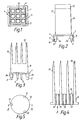
- the housing has a base portion 1 having spacers 2a, 3a and locating pins 2, 3, for the purpose of spacing the housing from, and locating the housing on printed circuit board.
- the locating pins 2, 3 may have different diameters to ensure that the housing can only be mounted in a particular orientation on the board.
- the base portion also has extended therefrom two retaining means 4, 5 in the form of resilient legs having an inclined surface 6 and a recess 7.
- the legs 4, 5 move towards each other as the inclined surface 6 makes contact with a hole within the board and once the inclined surface has fully passed through the hole in the board the legs return to their normal position and are thereby securely located with the recess 7 located under the board.
- the legs 4, 5 may be offset as shown in Figure 1 and Figure 3.
- the base portion 1 is provided with holes 10 passing therethrough for accommodating the light emitting diodes.
- the base portion 1 incorporates a light emitting diode holder 8 through which the holes 10 pass for the purpose of mounting the light emitting diodes.
- the diodes are arranged in three rows comprising three light emitting diodes.
- the holder 8 has four fins 11 which may be tapered, extending therefrom.
- the fins are 50mm in length.
- the tip of each fin is further tapered by an inclined surface 12.
- Each fin 11 extends across and above a row of light emitting diodes with the inclined surface 12 being on the underside of each fin 11.
- the fins 11 provide the shade for the light emitting diodes thus preventing them from reflecting sunlight when they are inactive.
- the inclined surface 12 reduces the surface area of the front edge of each fin from which light can be reflected
- the module is mounted so that when viewed, the fins 11 lie in a horizontal plane.
- each hole 10 includes a number of protrusions 13 which form a crushable grip for the light emitting diode.
- the grip deforms so that it can accommodate a light emitting diode having a diameter falling within a lower tolerance, and it deforms to a greater extent to accommodate a light emitting diode which has a tolerance falling within a higher tolerance. In this manner, all light emitting diodes which fall within the manufacturing tolerance range can be securely located within a respective hole 10 within the holder 8.
- FIG. 5 there is shown a view of a hole 10 when viewed in a direction of arrow X of Figure 4.
- Each hole 10 has three protrusions 13 equally spaced around the circumference of the hole.
- the protrusions are generally V shaped, terminating at a point which faces inwardly of the hole.
- the protrusions are arranged to deform or crush when a light emitting diode is inserted in the hole 10, thereby accommodating light emitting diodes having different diameters.
- the arrangement as discussed describes means which addresses a number of technical problems experienced with the use of light emitting diodes which form characters in a variable message display.
- the invention as described maximises character contrast ratio by reducing the value of the light output when the pixels are inactive. This is done in two ways, firstly, the light emitting diodes are shaded from the sun by the fins 11 as described above, and thus the light emitting diodes cannot reflect sunlight, and, secondly because the end of the fins 11 have a reduced surface area produced by the tapered region 12 as described above, the area of reflecting surface is therefore reduced.
- the light emitting diodes are manufactured with a lip, and conveniently this lip is used to ensure that each light emitting diode is aligned perpendicular to the character axis. This is achieved by ensuring that the light emitting diodes are fixed such that the lip of the light emitting diode is used as a mechanical reference point by fixing the light emitting diode with the lip hard against a flat surface of the holder 8 perpendicular to the character face.
- the light emitting diodes are usually fitted to the holder 8 from the direction of arrow X in Figure 4.
- the deformable protrusions 13 as described above accommodates a tolerance of plus/minus 0.5mm, whereby the protrusions 13 are deformed in respect of those diodes having a smaller diameter and will be deformed further in respect of those light emitting diodes having a larger diameter.
- the invention described lends itself to ease of assembly in that the light emitting diodes which need to be aligned before insertion into the printed circuit board is achievable by holding the light emitting diodes in the desired array orientated correctly for insertion into the printed circuit boards.
- each pixel may comprise more than nine light emitting diodes, and the deformable legs may be provided in different positions than shown.
Landscapes
- Engineering & Computer Science (AREA)
- Physics & Mathematics (AREA)
- General Physics & Mathematics (AREA)
- Theoretical Computer Science (AREA)
- General Engineering & Computer Science (AREA)
- Devices For Indicating Variable Information By Combining Individual Elements (AREA)
- Illuminated Signs And Luminous Advertising (AREA)
- Led Device Packages (AREA)
Applications Claiming Priority (2)
| Application Number | Priority Date | Filing Date | Title |
|---|---|---|---|
| GB9707675 | 1997-04-16 | ||
| GB9707675A GB2324363B (en) | 1997-04-16 | 1997-04-16 | Improvements in or relating to variable message displays |
Publications (2)
| Publication Number | Publication Date |
|---|---|
| EP0872822A2 true EP0872822A2 (de) | 1998-10-21 |
| EP0872822A3 EP0872822A3 (de) | 1999-12-01 |
Family
ID=10810861
Family Applications (1)
| Application Number | Title | Priority Date | Filing Date |
|---|---|---|---|
| EP98201077A Ceased EP0872822A3 (de) | 1997-04-16 | 1998-04-06 | Verbesserung im Bezug auf Anzeigevorrichtungen mit wechselnder Anzeige |
Country Status (3)
| Country | Link |
|---|---|
| EP (1) | EP0872822A3 (de) |
| CA (1) | CA2231730A1 (de) |
| GB (1) | GB2324363B (de) |
Cited By (2)
| Publication number | Priority date | Publication date | Assignee | Title |
|---|---|---|---|---|
| GB2324598B (en) * | 1997-04-21 | 2001-04-18 | Microsense Systems Ltd | A display |
| EP1645800A3 (de) * | 2004-10-07 | 2007-02-28 | Barco, naamloze vennootschap. | System und Verfahren zur optischen Verstärkung von Video- und Lichtelementen |
Family Cites Families (10)
| Publication number | Priority date | Publication date | Assignee | Title |
|---|---|---|---|---|
| US4471414A (en) * | 1982-03-11 | 1984-09-11 | Savage John Jun | Integrated light unit and circuit element attachable to circuit board |
| SE8501110L (sv) * | 1985-03-07 | 1986-09-08 | Torsten Lundin | Anordning vid en belyst yta, foretredesvis en ljusskylt |
| JPS64901A (en) * | 1987-06-24 | 1989-01-05 | Asahi Chem Ind Co Ltd | Material for constituting light shielding screen |
| US5268828A (en) * | 1991-04-19 | 1993-12-07 | Takiron Co., Ltd. | Illuminant display device |
| CA2108198A1 (en) * | 1992-10-13 | 1994-04-14 | David A. Donatello | Railway light signal |
| JP2755080B2 (ja) * | 1992-12-16 | 1998-05-20 | 松下電器産業株式会社 | Led表示器 |
| US5303124A (en) * | 1993-07-21 | 1994-04-12 | Avi Wrobel | Self-energizing LED lamp |
| JPH08287719A (ja) * | 1995-04-10 | 1996-11-01 | Copal Co Ltd | 発光装置 |
| JP3247821B2 (ja) * | 1995-05-24 | 2002-01-21 | シャープ株式会社 | 表示装置およびその製造方法 |
| IT232125Y1 (it) * | 1997-05-15 | 1999-11-30 | S I M S P A | Contenitore per dispositivi di visualizzazione di messaggi variabili |
-
1997
- 1997-04-16 GB GB9707675A patent/GB2324363B/en not_active Expired - Fee Related
-
1998
- 1998-04-06 EP EP98201077A patent/EP0872822A3/de not_active Ceased
- 1998-04-15 CA CA002231730A patent/CA2231730A1/en not_active Abandoned
Cited By (2)
| Publication number | Priority date | Publication date | Assignee | Title |
|---|---|---|---|---|
| GB2324598B (en) * | 1997-04-21 | 2001-04-18 | Microsense Systems Ltd | A display |
| EP1645800A3 (de) * | 2004-10-07 | 2007-02-28 | Barco, naamloze vennootschap. | System und Verfahren zur optischen Verstärkung von Video- und Lichtelementen |
Also Published As
| Publication number | Publication date |
|---|---|
| CA2231730A1 (en) | 1998-10-16 |
| GB9707675D0 (en) | 1997-06-04 |
| GB2324363A (en) | 1998-10-21 |
| GB2324363B (en) | 2001-05-16 |
| EP0872822A3 (de) | 1999-12-01 |
Similar Documents
| Publication | Publication Date | Title |
|---|---|---|
| US6502956B1 (en) | Light emitting diode lamp with individual LED lenses | |
| US5400229A (en) | Receptacle apparatus for light emitting diodes | |
| US5481440A (en) | Circuit pack with light pipes | |
| EP2716959B1 (de) | Lichtemittierende Vorrichtung | |
| US20030128531A1 (en) | Removable visual indication structure for a printed circuit board | |
| US10480768B2 (en) | Plastic heat sink for luminaires | |
| US20220053930A1 (en) | Low Voltage Power System for a Merchandise Display | |
| AU4261100A (en) | Light-emitting diode arrangement | |
| US20060171148A1 (en) | LED signboard mounting structure | |
| US6113280A (en) | Cap for optical connector | |
| US7264383B2 (en) | Lighting element with a light emitting device | |
| EP1742522A3 (de) | Diodenmodul für Beleuchtungsanordnung, Rückbeleuchtungsanordnung und Anzeigevorrichtung damit | |
| EP0872822A2 (de) | Verbesserung im Bezug auf Anzeigevorrichtungen mit wechselnder Anzeige | |
| JP4746152B1 (ja) | 表示体用照明装置 | |
| US6360999B1 (en) | LED indicator retaining device | |
| EP3132184B1 (de) | Flexibles band-led-modul | |
| US5123857A (en) | Electrical connector embedded with metal latches | |
| KR200211994Y1 (ko) | 광섬유 고정장치 | |
| EP1544951B1 (de) | Elektrischer Verbinder | |
| JP4043090B2 (ja) | 発光ダイオード表示器 | |
| JP4173591B2 (ja) | 発光ダイオード表示器 | |
| KR101587987B1 (ko) | 기호형태의 천공 표시부를 이용한 도로교통안내판 | |
| EP1055557A2 (de) | Fahrzeug-Beleuchtungseinrichtung mit einer Vielzahl von Leuchtdioden | |
| JPH0432890A (ja) | 発光ダイオード表示素子 | |
| US5492477A (en) | Miniature lamp holder |
Legal Events
| Date | Code | Title | Description |
|---|---|---|---|
| PUAI | Public reference made under article 153(3) epc to a published international application that has entered the european phase |
Free format text: ORIGINAL CODE: 0009012 |
|
| AK | Designated contracting states |
Kind code of ref document: A2 Designated state(s): DE NL |
|
| AX | Request for extension of the european patent |
Free format text: AL;LT;LV;MK;RO;SI |
|
| 17P | Request for examination filed |
Effective date: 19981218 |
|
| PUAL | Search report despatched |
Free format text: ORIGINAL CODE: 0009013 |
|
| AK | Designated contracting states |
Kind code of ref document: A3 Designated state(s): AT BE CH CY DE DK ES FI FR GB GR IE IT LI LU MC NL PT SE |
|
| AX | Request for extension of the european patent |
Free format text: AL;LT;LV;MK;RO;SI |
|
| AKX | Designation fees paid |
Free format text: DE NL |
|
| 17Q | First examination report despatched |
Effective date: 20010123 |
|
| GRAG | Despatch of communication of intention to grant |
Free format text: ORIGINAL CODE: EPIDOS AGRA |
|
| STAA | Information on the status of an ep patent application or granted ep patent |
Free format text: STATUS: THE APPLICATION HAS BEEN REFUSED |
|
| 18R | Application refused |
Effective date: 20020930 |