EP0872874A1 - Mehrelektroden-Partikeldetektor und Herstellungsverfahren desselben - Google Patents
Mehrelektroden-Partikeldetektor und Herstellungsverfahren desselben Download PDFInfo
- Publication number
- EP0872874A1 EP0872874A1 EP98400930A EP98400930A EP0872874A1 EP 0872874 A1 EP0872874 A1 EP 0872874A1 EP 98400930 A EP98400930 A EP 98400930A EP 98400930 A EP98400930 A EP 98400930A EP 0872874 A1 EP0872874 A1 EP 0872874A1
- Authority
- EP
- European Patent Office
- Prior art keywords
- electrode
- detector
- border
- elements
- electrodes
- Prior art date
- Legal status (The legal status is an assumption and is not a legal conclusion. Google has not performed a legal analysis and makes no representation as to the accuracy of the status listed.)
- Granted
Links
Images


Classifications
-
- H—ELECTRICITY
- H01—ELECTRIC ELEMENTS
- H01J—ELECTRIC DISCHARGE TUBES OR DISCHARGE LAMPS
- H01J47/00—Tubes for determining the presence, intensity, density or energy of radiation or particles
- H01J47/001—Details
-
- H—ELECTRICITY
- H01—ELECTRIC ELEMENTS
- H01J—ELECTRIC DISCHARGE TUBES OR DISCHARGE LAMPS
- H01J47/00—Tubes for determining the presence, intensity, density or energy of radiation or particles
- H01J47/02—Ionisation chambers
Definitions
- the present invention relates to a detector of particles with multiple electrodes as well as a manufacturing process of this detector.
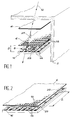
- Figure 1 is a perspective view schematic and partial of an embodiment particular of this known detector.
- the electrode 6 constitutes the cathode of the detector while the electrode 8 constitutes the anode of this detector.
- the electrode 4 the structure of which matters little (it can be for example a grid), and the cathode 6 of the detector of figure 1 delimit a space called "conversion space”.
- the cathode 6 and the anode 8 of the detector define, for their part, a space called "space amplification ".
- the anode 8 of the detector comprises a set elementary anodes 14 formed on a support electrically insulating 16 and spaced from each other other.
- these elementary anodes are electrically bands conductors parallel to each other.
- the cathode 6 of the detector of FIG. 1 is an electrically conductive thin plate, of thin and pierced with holes 18 of small size, this cathode 6 thus forming a grid which, given the small size of its holes, may be called "micro-grid”.
- Polarization means not shown are able to bring the electrode 4 to a potential HV1, cathode 6 at a potential HV2 greater than HV1 and all conductive strips 14 at the same potential HV3 higher than HV2.
- the polarization means make it possible to create electric fields El and E2 respectively in conversion space and in space amplification.
- the distance D between cathode 6 and the plane conductive strip 14 is weak.
- the distance D is worth 100 ⁇ m.
- the distance between electrode 4 and the cathode 6 is much larger and is 3 mm in the example shown.
- the ratio R of the intensity of the electric field E2, created in space amplification, at the intensity of the electric field E1, created in the conversion space is very large in front 1 (greater than 10).
- the polarization means generate a field of 50 kV / cm in the amplification space and a field of 1 kV / cm in the conversion space so that ratio R is equal to 50.
- the conductive strips 14 are copper micro-tracks 150 ⁇ m wide and 5 ⁇ m thick (thickness much lower than D), which are formed by a classic technique of photogravure on the substrate insulator 16, these micro-tracks being spaced apart others of 320 ⁇ m.
- the micro-grid 6 is formed by electrodeposition and has a thickness of the order of 3 ⁇ m to 4 ⁇ m and square holes of 15 ⁇ m x 15 ⁇ m with a pitch of 25 ⁇ m.
- the enclosure 2 of the detector of FIG. 1 is provided with means not shown allowing it circulate a suitable gas, for example a mixture Ar + 10% DME.
- this gas allows the amplification of electrons by a process avalanche.
- the gas does not circulate at through enclosure 2 but enclosure 2 is initially filled with gas at the desired pressure.
- Each of the micro-tracks 14 is connected to a fast amplifier not shown, allowing amplify the electrical signals collected by this micro-track.
- an ionizing particle 12 crosses the conversion space defined by the electrodes 4 and 6, it ionizes the gas which is in the space of conversion and creates about ten electrons there primary.
- This crossing of the micro-grid is facilitated by the high R ratio existing between the field created in the conversion space and the field created in the amplification space.
- the field lines are deformed in the vicinity of the micro-grid and the electrons are focused towards the center of the holes in this micro-grid.
- these electrons are amplified by the well known process thanks to the high field prevailing in the amplification space (associated with the gas mixture suitable, e.g. Ar + 10% DME).
- Electrons are collected in a few nanoseconds by the anode micro-tracks and the ions quickly drift towards the micro-grid.
- the ion drift creates by induction a load on the micro-tracks of the anode.
- micro-tracks whose pitch is around of the amplification interval allow a location of the avalanche.
- M e ⁇ D
- ⁇ the first Townsend coefficient
- E2 the electric field created in the amplification space
- D the distance between the micro-grid and the anode where the multiplication.
- the variation of the gain M in function of V is substantially exponential when V varies in the range from 0.2kV to 0.5kV.
- the gain of detector is insensitive to small variations in distance between the micro-grid and the anode.
- This attraction tends to distort the micro-grid and can modify the amplification space if this micro-grid is not sufficiently maintained.
- electrically insulating spacers 29 (figure 2) made up of quartz or nylon fibers, the diameter is equal to D (100 ⁇ m) and which are placed on the micro-tracks 14 of the anode, perpendicular to these micro-tracks, and are regularly spaced from each other with a pitch ⁇ of the order of 2 mm at 3 mm.
- micro-grid thus stretched is placed on the fibers forming the spacers, the micro-grid being then between the frame and these fibers.
- the micro-grid holding frame presenting his own faults and his own rigidity, it appears areas where the distance between the micro-grid and the anode is no longer equal to its value nominal.
- the central part of the latter far from the support frame, usually has no defect because the micro-grid, stretched by the cnamp electric, rests well on the fibers.
- the object of the present invention is to remedy the above drawbacks and, more generally prevent a flexible electrode from a particle detector to come into contact with a other electrode of this detector under the effect of a electrostatic force resulting from the application of a electrical voltage between these two electrodes while disturbing the electric field less than before thus established between these two electrodes.
- the present invention has for object an electrode particle detector multiple, in which a flexible electrode and a other electrode are intended to be worn at different electrical potentials and are maintained spaced from each other by spacers electrically insulating, placed between these two electrodes, this detector being characterized in that the spacers are point elements, distributed in the space between the two electrodes.
- the detector may further include a electrically insulating border which surrounds the whole point elements.
- Point elements and / or border can be attached to said other electrode, the flexible electrode resting on the elements punctual and possibly attached to the border.
- the two electrodes are kept parallel to the means of the elements punctual, these then having the same height (equal to the desired distance between the two electrodes).
- the border if used, has the same height than point elements.
- the present invention applies all particularly to detectors like those are described in documents (1), (2) and (3) mentioned above:
- the detector object of the invention can further comprise a first electrode spaced from the two electrodes, the flexible electrode delimiting (a) with said other electrode an amplification space where these two electrodes respectively constitute a cathode and an anode and (b) with the first electrode a space for converting particles into electrons ionization and drift of these electrons towards the amplification space, the cathode being pierced with holes, the anode comprising a set of anodes electrically isolated from each other others, the first electrode being intended to be brought to a first potential, the cathode to a second potential greater than the first potential and the anodes elementary to a third potential greater than second potential, to create electric fields respectively in the conversion spaces and amplification.
- the first electrode, the anode and the cathode are the distance D between the cathode and the anode being less than 500 ⁇ m, the ratio R of the intensity of the electric field created in the amplification space to the intensity of the electric field created in the space of conversion being greater than 10, the height of point elements being equal to D and the dimensions of these point elements, counted parallel to the anode, being substantially equal to D.
- anode and cathode point elements and / or the border are preferably fixed to the anode and the cathode rests on the point elements, and is possibly attached to the border.
- the distance between the flexible electrode and said other electrode is not not constant, these two electrodes being spaced apart controlled way using height spacers adapted to the desired interval between these two electrodes.
- the point elements form cylinders (in the broad sense, the cylinders of revolution being only a particular case), each cylinder having dimensions which, counted parallel to said two electrodes, are substantially equal to or less than the height of this cylinder.
- the point elements form spheres.
- the present invention also relates to a manufacturing process of the object detector the invention, characterized in that the said form is formed other electrode a layer of photoresist (resin photosensitive) whose thickness is adapted to the space chosen between the two electrodes, in that we form these point elements by insolation of this layer, through a mask defining the point elements, then development of the layer, and in that we place then the flexible electrode on the point elements in photoresist thus formed.
- photoresist resin photosensitive
- the photoresist layer is formed on the anode of the detector, so as to form thereon the point elements in photoresist, and the cathode is then placed on these point elements in photoresist.
- the mask further defines said border, so as to also form a border in photoresist on the anode by insolation then development of the photoresist layer and we place then the cathode on the point elements in photoresist.
- the thickness is equal to this height.
- these columns are regularly distributed in the space between the anode and the micro-grid and we note ⁇ the pitch of balusters.
- the disturbed area represents ( ⁇ / 4). (3D / ⁇ ) 2 of the detector surface.
- the ratio D / rapport occurs at square and, keeping a step ⁇ between columns of 2 mm, only 1.7% of the detector surface is disturbed.
- balusters instead of fibers therefore leads to a considerable reduction in the disturbed surface.
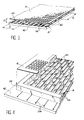
- Columns 30 could be formed on the insulating substrate 16 but, in the example shown, they are formed on micro-tracks conductive 14.
- the detector according to the invention which is shown schematically and partial in Figure 3, we start by forming the micro-grid and the substrate (e.g. resin epoxy) carrying the micro-tracks 14 which are obtained by a traditional photogravure technique.
- the substrate e.g. resin epoxy
- the columns 30 are then formed also by a photoengraving technique.
- the thickness of this layer is equal to the distance D desired and can range from 50 ⁇ m to 100 ⁇ m (it is worth 100 ⁇ m in the example considered).
- This mask is previously aligned with the surface carrying the conductive micro-tracks using of marks engraved at the same time as these micro-tracks conductive.
- the detector is then completed (in particular by installing micro-grid 6 and the electrode 4).
- a photoresist border 32 (FIG. 4) which surrounds all of the balusters 30 and has the same height D than these.
- the micro-grid 6 When mounting the detector, the micro-grid 6 is placed on the balusters 30 and then stretched and fixed at its periphery on the edge 32, of preferably by gluing for example by means of a epoxy resin.
- the conductors 34 which can be seen on the figure 4 are simply extensions of the micro-tracks conductive and allow the connection of these to fast amplifiers that we use during the operation of the detector as we have seen upper.
- Such a detector according to the invention does not shows no disturbances comparable to those that we observed with detectors using fibers as spacers.
- balusters The area covered by the balusters is much less than in the prior art since we are gone from a linear configuration to a configuration punctual.
- the flatness defects of the substrate 16 are tolerable.
- the amount of material introduced into the detector is also weaker than in art conversion space can be reduced if necessary.
- a wide range of film thicknesses from photoresist is commercially available and all kinds of patterns are possible at the time of photogravure.
- the spacers can be shaped cylindrical of revolution or parallelepiped by example.
- a detector formed with the process using a photoresist layer still allows a change of micro-grid provided you use a glue easy to dissolve without damaging the photoresist.
- the micro-grid 6 is no longer attached to border 32: it is attached to substrate 16 using the border as spacer.
- the micro-grid can then be easily connected to a bias electrode: on can provide a photo-etched electrode on the substrate and use a conductive glue to fix the micro-grid to the substrate and, in particular, to this electrode.
- Attachment of the micro-grid to the substrate has another advantage: when you want to place two detectors side by side on the same insulating substrate, the fixing of the two corresponding micro-grids on this substrate reduces the “dead zone” between these two micro-grids.
- two detectors 36 and 38 are formed on the same substrate 16.
- micro-grids 6 and 6a rest on the posts 30 and 30a and borders 32 and 32a corresponding and are fixed, by gluing, to the substrate 16, in space 40.
- elementary anodes forming parallel micro-tracks 14 we can use, as mentioned in the document (1), elementary anodes forming a network two-dimensional checkerboard on the insulating substrate 16 or any other configuration.
- spheres insulators of diameter D, for example quartz, to the place of these balusters.
- the invention applies to any detector of particles in which two electrodes must be kept parallel to each other.
- the thickness of the micro-grid is of the order of 3 ⁇ m to 4 ⁇ m but in other detectors it could go up to 100 ⁇ m.
- the invention applies to any electrode liable to deform (whatever its thickness), to prevent it from forming a short circuit with another adjacent electrode by electro-static attraction with the latter when an electrical voltage is applied between these two electrodes.
- the electrodes are also not necessarily parallel.
- it may be useful to do continuously vary the distance between the micro-grid and the anode of a MICROMEGAS type detector (documents (1) to (3)).
- a MICROMEGAS type detector (documents (1) to (3)).
- spacers points of varying heights are achievable by example using insulating balls with diameters variables or by means of photoresist and a photolithography, and allow, thanks to the flexibility of the microgrid, to get any space desired between this microgrid and the anode.
Landscapes
- Measurement Of Radiation (AREA)
- Investigating Or Analyzing Materials By The Use Of Electric Means (AREA)
Applications Claiming Priority (2)
| Application Number | Priority Date | Filing Date | Title |
|---|---|---|---|
| FR9704617 | 1997-04-15 | ||
| FR9704617A FR2762096B1 (fr) | 1997-04-15 | 1997-04-15 | Detecteur de particules a electrodes paralleles multiples et procede de fabrication de ce detecteur |
Publications (2)
| Publication Number | Publication Date |
|---|---|
| EP0872874A1 true EP0872874A1 (de) | 1998-10-21 |
| EP0872874B1 EP0872874B1 (de) | 2002-12-18 |
Family
ID=9505917
Family Applications (1)
| Application Number | Title | Priority Date | Filing Date |
|---|---|---|---|
| EP98400930A Expired - Lifetime EP0872874B1 (de) | 1997-04-15 | 1998-04-15 | Mehrelektroden-Partikeldetektor und Herstellungsverfahren desselben |
Country Status (4)
| Country | Link |
|---|---|
| EP (1) | EP0872874B1 (de) |
| AT (1) | ATE230159T1 (de) |
| DE (1) | DE69810182T2 (de) |
| FR (1) | FR2762096B1 (de) |
Cited By (3)
| Publication number | Priority date | Publication date | Assignee | Title |
|---|---|---|---|---|
| EP1343194A1 (de) * | 2002-03-08 | 2003-09-10 | Biospace Instruments | Strahlungsdetektoren und autoradiographische Abbildungsvorrichtungen mit solcher Detektoren |
| EP2317538A1 (de) | 2009-10-28 | 2011-05-04 | CERN - European Organization For Nuclear Research | Verfahren zur Erstellung eines Verstärkungsraums eines Lawinenteilchendetektors |
| EP2562563A1 (de) | 2011-08-26 | 2013-02-27 | CERN - European Organization For Nuclear Research | Detektorausleseschnittstelle für einen Lawinenteilchendetektor |
Families Citing this family (2)
| Publication number | Priority date | Publication date | Assignee | Title |
|---|---|---|---|---|
| FR2790100B1 (fr) | 1999-02-24 | 2001-04-13 | Commissariat Energie Atomique | Detecteur bidimensionnel de rayonnements ionisants et procede de fabrication de ce detecteur |
| US20260011522A1 (en) * | 2024-07-03 | 2026-01-08 | Varex Imaging Corporation | Gridded cathode apparatuses and x-ray systems |
Citations (3)
| Publication number | Priority date | Publication date | Assignee | Title |
|---|---|---|---|---|
| JPS58188030A (ja) * | 1982-04-26 | 1983-11-02 | Fujitsu Ltd | ガス放電パネルの製造方法 |
| GB2141577A (en) * | 1983-06-16 | 1984-12-19 | American Telephone & Telegraph | Improvements in or relating to display devices |
| EP0622826A1 (de) * | 1993-04-28 | 1994-11-02 | Hamamatsu Photonics K.K. | Photovervielfacher |
-
1997
- 1997-04-15 FR FR9704617A patent/FR2762096B1/fr not_active Expired - Fee Related
-
1998
- 1998-04-15 DE DE69810182T patent/DE69810182T2/de not_active Expired - Lifetime
- 1998-04-15 EP EP98400930A patent/EP0872874B1/de not_active Expired - Lifetime
- 1998-04-15 AT AT98400930T patent/ATE230159T1/de not_active IP Right Cessation
Patent Citations (3)
| Publication number | Priority date | Publication date | Assignee | Title |
|---|---|---|---|---|
| JPS58188030A (ja) * | 1982-04-26 | 1983-11-02 | Fujitsu Ltd | ガス放電パネルの製造方法 |
| GB2141577A (en) * | 1983-06-16 | 1984-12-19 | American Telephone & Telegraph | Improvements in or relating to display devices |
| EP0622826A1 (de) * | 1993-04-28 | 1994-11-02 | Hamamatsu Photonics K.K. | Photovervielfacher |
Non-Patent Citations (2)
| Title |
|---|
| GIOMATARIS Y ET AL: "MICROMEGAS: a high-granularity position-sensitive gaseous detector for high particle-flux environments", NUCLEAR INSTRUMENTS & METHODS IN PHYSICS RESEARCH, SECTION A (ACCELERATORS, SPECTROMETERS, DETECTORS AND ASSOCIATED EQUIPMENT), 21 JUNE 1996, ELSEVIER, NETHERLANDS, vol. 376, no. 1, ISSN 0168-9002, pages 29 - 35, XP002050622 * |
| PATENT ABSTRACTS OF JAPAN vol. 008, no. 025 (E - 225) 2 February 1984 (1984-02-02) * |
Cited By (6)
| Publication number | Priority date | Publication date | Assignee | Title |
|---|---|---|---|---|
| EP1343194A1 (de) * | 2002-03-08 | 2003-09-10 | Biospace Instruments | Strahlungsdetektoren und autoradiographische Abbildungsvorrichtungen mit solcher Detektoren |
| FR2837000A1 (fr) * | 2002-03-08 | 2003-09-12 | Biospace Instr | Detecteurs de radiations et dispositifs d'imagerie autoradiographique comprenant de tels detecteurs |
| EP2317538A1 (de) | 2009-10-28 | 2011-05-04 | CERN - European Organization For Nuclear Research | Verfahren zur Erstellung eines Verstärkungsraums eines Lawinenteilchendetektors |
| US9111737B2 (en) | 2009-10-28 | 2015-08-18 | CERN—European Organization for Nuclear Research | Method for fabricating an amplification gap of an avalanche particle detector |
| EP2562563A1 (de) | 2011-08-26 | 2013-02-27 | CERN - European Organization For Nuclear Research | Detektorausleseschnittstelle für einen Lawinenteilchendetektor |
| WO2013029748A1 (en) | 2011-08-26 | 2013-03-07 | Cern - European Organization For Nuclear Research | Detector-readout interface for an avalanche particle detector |
Also Published As
| Publication number | Publication date |
|---|---|
| FR2762096A1 (fr) | 1998-10-16 |
| FR2762096B1 (fr) | 1999-06-11 |
| DE69810182T2 (de) | 2003-10-09 |
| ATE230159T1 (de) | 2003-01-15 |
| DE69810182D1 (de) | 2003-01-30 |
| EP0872874B1 (de) | 2002-12-18 |
Similar Documents
| Publication | Publication Date | Title |
|---|---|---|
| EP0855086B1 (de) | Lage empfindlicher hochanflösungs detektor für hohe flüsse ionisierender teilchen | |
| FR2812455A1 (fr) | Detecteur de photon unique supraconducteur | |
| EP0272178A1 (de) | Spinpolarisierte Elektronenquelle unter Verwendung einer aus mehrere Mikrospitzen bestehenden Emissionskathode, Verwendung in der Physik der Elektronen-Materie- oder Elektronen-Partikel-Wechselwirkungen, in der Plasmaphysik, in der Elektronenmikroskopie | |
| FR2541784A1 (fr) | Dispositif de deflexion statique d'un faisceau infra-rouge | |
| EP0228933B1 (de) | Vorrichtung zur Wahrnehmung und Lokalisierung von neutralen Partikeln und deren Anwendung | |
| FR2631132A1 (fr) | Detecteur d'images radiologiques | |
| EP0872874B1 (de) | Mehrelektroden-Partikeldetektor und Herstellungsverfahren desselben | |
| WO2011039330A1 (fr) | Dispositif et methode pour le controle en ligne d'un faisceau energetique | |
| EP2786426A1 (de) | Halbleiterstruktur zur aufnahme von elektromagnetischer strahlung, halbleiterbauelement und verfahren zur herstellen einer solchen halbleiterstruktur | |
| WO1993003495A1 (fr) | Detecteur a gaz de rayonnement ionisant | |
| EP3234652A1 (de) | Verfahren zur herstellung eines neutronendetektors und neutronendetektor | |
| WO2003010793A1 (fr) | Detecteur de rayonnements ionisants, a lame solide de conversion des rayonnements, et procede de fabrication de ce detecteur | |
| FR2557361A1 (fr) | Boitier de detecteur d'ionisation, son procede de fabrication et detecteur d'ionisation utilisant un tel boitier | |
| FR2639436A1 (fr) | Procede et dispositif de localisation de particules neutres, a haute resolution | |
| FR2557363A1 (fr) | Procede de fabrication d'un detecteur d'ionisation et detecteur ainsi fabrique | |
| FR2780203A1 (fr) | Detecteur a puits quantique avec couche de stockage des electrons photoexcites | |
| WO1998014981A1 (fr) | Detecteur a gaz de rayonnements ionisants a tres grand taux de comptage | |
| EP1186058A1 (de) | Strahlungsdetektor mit grossem dynamischen bereich | |
| EP1343194A1 (de) | Strahlungsdetektoren und autoradiographische Abbildungsvorrichtungen mit solcher Detektoren | |
| EP0441853B1 (de) | Verfahren und vorrichtung zur bidimensionalen lokalisierung nichtgeladener partikel, insbesondere bei geringer zählrate | |
| FR2608842A1 (fr) | Transducteur photo-electronique utilisant une cathode emissive a micropointes | |
| FR3069700A1 (fr) | Chambre a fission a anode segmentee | |
| FR2557362A1 (fr) | Procede de fabrication d'un reseau d'elements detecteurs pour un detecteur d'ionisation | |
| Pouthas | High spatial and time resolutions with gas ionization detectors | |
| WO2000030150A1 (fr) | Detecteur de localisation de photons, a remplissage gazeux |
Legal Events
| Date | Code | Title | Description |
|---|---|---|---|
| PUAI | Public reference made under article 153(3) epc to a published international application that has entered the european phase |
Free format text: ORIGINAL CODE: 0009012 |
|
| AK | Designated contracting states |
Kind code of ref document: A1 Designated state(s): AT CH DE FR GB IT LI NL |
|
| AX | Request for extension of the european patent |
Free format text: AL;LT;LV;MK;RO;SI |
|
| 17P | Request for examination filed |
Effective date: 19990331 |
|
| RAP1 | Party data changed (applicant data changed or rights of an application transferred) |
Owner name: BIOSPACE INSTRUMENTS Owner name: CHARPAK, GEORGES Owner name: COMMISSARIAT A L'ENERGIE ATOMIQUE |
|
| AKX | Designation fees paid |
Free format text: AT CH DE FR GB IT LI NL |
|
| RAP1 | Party data changed (applicant data changed or rights of an application transferred) |
Owner name: BIOSPACE INSTRUMENTS Owner name: COMMISSARIAT A L'ENERGIE ATOMIQUE |
|
| 17Q | First examination report despatched |
Effective date: 20001207 |
|
| GRAG | Despatch of communication of intention to grant |
Free format text: ORIGINAL CODE: EPIDOS AGRA |
|
| GRAG | Despatch of communication of intention to grant |
Free format text: ORIGINAL CODE: EPIDOS AGRA |
|
| GRAH | Despatch of communication of intention to grant a patent |
Free format text: ORIGINAL CODE: EPIDOS IGRA |
|
| GRAH | Despatch of communication of intention to grant a patent |
Free format text: ORIGINAL CODE: EPIDOS IGRA |
|
| GRAA | (expected) grant |
Free format text: ORIGINAL CODE: 0009210 |
|
| AK | Designated contracting states |
Kind code of ref document: B1 Designated state(s): AT CH DE FR GB IT LI NL |
|
| REF | Corresponds to: |
Ref document number: 230159 Country of ref document: AT Date of ref document: 20030115 Kind code of ref document: T |
|
| REG | Reference to a national code |
Ref country code: GB Ref legal event code: FG4D Free format text: NOT ENGLISH |
|
| REG | Reference to a national code |
Ref country code: CH Ref legal event code: EP |
|
| REF | Corresponds to: |
Ref document number: 69810182 Country of ref document: DE Date of ref document: 20030130 Kind code of ref document: P Ref document number: 69810182 Country of ref document: DE Date of ref document: 20030130 |
|
| GBT | Gb: translation of ep patent filed (gb section 77(6)(a)/1977) |
Effective date: 20030401 |
|
| PLBE | No opposition filed within time limit |
Free format text: ORIGINAL CODE: 0009261 |
|
| STAA | Information on the status of an ep patent application or granted ep patent |
Free format text: STATUS: NO OPPOSITION FILED WITHIN TIME LIMIT |
|
| 26N | No opposition filed |
Effective date: 20030919 |
|
| PGFP | Annual fee paid to national office [announced via postgrant information from national office to epo] |
Ref country code: AT Payment date: 20060412 Year of fee payment: 9 |
|
| PG25 | Lapsed in a contracting state [announced via postgrant information from national office to epo] |
Ref country code: AT Free format text: LAPSE BECAUSE OF NON-PAYMENT OF DUE FEES Effective date: 20070415 |
|
| REG | Reference to a national code |
Ref country code: FR Ref legal event code: CD Owner name: EOS IMAGING, FR Effective date: 20111213 Ref country code: FR Ref legal event code: CA Effective date: 20111213 |
|
| REG | Reference to a national code |
Ref country code: NL Ref legal event code: TD Effective date: 20120131 |
|
| REG | Reference to a national code |
Ref country code: CH Ref legal event code: PFA Owner name: COMMISSARIAT A L'ENERGIE ATOMIQUE Free format text: COMMISSARIAT A L'ENERGIE ATOMIQUE#31-33, RUE DE LA FEDERATION#75015 PARIS (FR) $ BIOSPACE INSTRUMENTS#104 BOULEVARD AUGUSTE BLANQUI#75013 PARIS (FR) -TRANSFER TO- COMMISSARIAT A L'ENERGIE ATOMIQUE#31-33, RUE DE LA FEDERATION#75015 PARIS (FR) $ EOS IMAGING#10, RUE MERCOEUR#75011 PARIS (FR) |
|
| PGFP | Annual fee paid to national office [announced via postgrant information from national office to epo] |
Ref country code: GB Payment date: 20130415 Year of fee payment: 16 Ref country code: DE Payment date: 20130409 Year of fee payment: 16 |
|
| PGFP | Annual fee paid to national office [announced via postgrant information from national office to epo] |
Ref country code: NL Payment date: 20130313 Year of fee payment: 16 |
|
| REG | Reference to a national code |
Ref country code: DE Ref legal event code: R119 Ref document number: 69810182 Country of ref document: DE |
|
| REG | Reference to a national code |
Ref country code: NL Ref legal event code: V1 Effective date: 20141101 |
|
| GBPC | Gb: european patent ceased through non-payment of renewal fee |
Effective date: 20140415 |
|
| REG | Reference to a national code |
Ref country code: DE Ref legal event code: R119 Ref document number: 69810182 Country of ref document: DE Effective date: 20141101 |
|
| PG25 | Lapsed in a contracting state [announced via postgrant information from national office to epo] |
Ref country code: GB Free format text: LAPSE BECAUSE OF NON-PAYMENT OF DUE FEES Effective date: 20140415 Ref country code: DE Free format text: LAPSE BECAUSE OF NON-PAYMENT OF DUE FEES Effective date: 20141101 |
|
| PG25 | Lapsed in a contracting state [announced via postgrant information from national office to epo] |
Ref country code: NL Free format text: LAPSE BECAUSE OF NON-PAYMENT OF DUE FEES Effective date: 20141101 |
|
| REG | Reference to a national code |
Ref country code: FR Ref legal event code: PLFP Year of fee payment: 19 |
|
| REG | Reference to a national code |
Ref country code: FR Ref legal event code: PLFP Year of fee payment: 20 |
|
| PGFP | Annual fee paid to national office [announced via postgrant information from national office to epo] |
Ref country code: CH Payment date: 20170424 Year of fee payment: 20 Ref country code: FR Payment date: 20170428 Year of fee payment: 20 |
|
| PGFP | Annual fee paid to national office [announced via postgrant information from national office to epo] |
Ref country code: IT Payment date: 20170411 Year of fee payment: 20 |
|
| REG | Reference to a national code |
Ref country code: CH Ref legal event code: PL |