EP0873577B1 - Antenne en spirale a fentes a source primaire et symetriseur integres - Google Patents
Antenne en spirale a fentes a source primaire et symetriseur integres Download PDFInfo
- Publication number
- EP0873577B1 EP0873577B1 EP96946132A EP96946132A EP0873577B1 EP 0873577 B1 EP0873577 B1 EP 0873577B1 EP 96946132 A EP96946132 A EP 96946132A EP 96946132 A EP96946132 A EP 96946132A EP 0873577 B1 EP0873577 B1 EP 0873577B1
- Authority
- EP
- European Patent Office
- Prior art keywords
- slot
- microstrip
- antenna apparatus
- spiral
- spiral antenna
- Prior art date
- Legal status (The legal status is an assumption and is not a legal conclusion. Google has not performed a legal analysis and makes no representation as to the accuracy of the status listed.)
- Expired - Lifetime
Links
Images




Classifications
-
- H—ELECTRICITY
- H01—ELECTRIC ELEMENTS
- H01Q—ANTENNAS, i.e. RADIO AERIALS
- H01Q9/00—Electrically-short antennas having dimensions not more than twice the operating wavelength and consisting of conductive active radiating elements
- H01Q9/04—Resonant antennas
- H01Q9/16—Resonant antennas with feed intermediate between the extremities of the antenna, e.g. centre-fed dipole
- H01Q9/26—Resonant antennas with feed intermediate between the extremities of the antenna, e.g. centre-fed dipole with folded element or elements, the folded parts being spaced apart a small fraction of operating wavelength
- H01Q9/27—Spiral antennas
-
- H—ELECTRICITY
- H01—ELECTRIC ELEMENTS
- H01Q—ANTENNAS, i.e. RADIO AERIALS
- H01Q13/00—Waveguide horns or mouths; Slot antennas; Leaky-waveguide antennas; Equivalent structures causing radiation along the transmission path of a guided wave
- H01Q13/10—Resonant slot antennas
- H01Q13/16—Folded slot antennas
-
- H—ELECTRICITY
- H01—ELECTRIC ELEMENTS
- H01Q—ANTENNAS, i.e. RADIO AERIALS
- H01Q13/00—Waveguide horns or mouths; Slot antennas; Leaky-waveguide antennas; Equivalent structures causing radiation along the transmission path of a guided wave
- H01Q13/10—Resonant slot antennas
- H01Q13/18—Resonant slot antennas the slot being backed by, or formed in boundary wall of, a resonant cavity ; Open cavity antennas
Definitions
- the present invention relates to planar, broadband antennas. More particularly, the present invention relates to slot spiral antennas having an integrated balun and feed.
- Spiral antennas are particularly known for their ability to produce very broadband, almost perfectly circularly-polarized radiation over their full coverage region. Because of this polarization diversity and broad spatial and frequency coverage, many different applications exist, ranging from military surveillance, ECM, and ECCM uses, to numerous commercial and private uses, including the consolidation of multiple low gain communications antennas on moving vehicles.
- spiral antenna are made of wire.
- the performance advantages mentioned above come at the price of size and complexity.
- the radiating elements of a wire spiral may be planar, the feed network and balun structure generally are not, and combine to add weight, depth, and significant complexity to the system.
- an absorbing cavity is generally used to eliminate the radiation in one direction, adding even more depth to the antenna.
- U.S. Patent # 3,760,420 to Hadad discloses a system for tracking the direction of a source of electromagnetic radiation.
- Hadad describes a conducting strip embedded in a dielectric material.
- the conducting strip is not a microstrip and is not formed on the substrate of a material, rather it is incorporated in the surrounding mass of a dielectric material.
- GB Patent # 2,005,083 to Bagley discloses a variable phase shifter for use at microwave frequencies having a first antenna arranged to emit circularly polarized waves from a microwave source and a second antenna for receiving waves.
- the antennae are configured as spirals and utilize a coaxial cable as a feed.
- the International Journal of Infrared and Millimeter Waves, Vol. 14 No. 10 October 1993 discloses a spiral self-complimentary antenna rather than a slot antenna and also utilizes a coaxial cable as a feed.
- the present invention provides a slot spiral antenna with an integrated matched planar balun and feed.
- One object of the present invention is to provide an improved simple broadband slot spiral antenna.
- Another object of the present invention is to provide a spiral antenna which can easily be incorporated into the skin of a moving vehicle in a streamlined/aerodynamic manner, without hindering the radiation of the antenna.
- Still another object of the present invention is to provide a slot spiral antenna which be easily miniaturized and which can shape and steer its radiation pattern.
- a further object of the present invention is to provide a uni-directional spiral antenna with an integrated balun and feed which is simple, thin, light and flexible.
- a still further object of the present invention is to provide a spiral antenna having a balanced feed, impedance matching both between the feed and the radiating element and at the input port and properly terminated antenna arms.
- the present invention provides a slot spiral antenna with an integrated planar balun and feed.
- the slot spiral antenna is produced using standard printed circuit techniques. It comprises a conducting layer formed on a material substrate. The conducting layer is etched or milled to form a radiating spiral slot. Any type or combination of types of spiral may be used, however, the preferred embodiment uses an Archimedean spiral. If necessary, to limit the spiral radiation to one direction, a cavity may also be included.
- the balun structure comprises a microstrip line that winds toward the center of the slot spiral.
- the feed is executed by breaking the ground plane of the microstrip line with the spiral slot.
- the impedance of the slotline is chosen to be twice that of the microstrip line.
- the microstrip line sees the slotline as a pair of shunt branches, and thus the slotline impedance yields a perfect match at the feed.
- the microstrip line continues past the microstrip/slotline transition and winds back out from the center of the slot spiral where it is terminated in any one of several ways.
- the slot spiral antenna apparatus of the present invention includes a material substrate 12, having conductive layers on both sides. On one side, a portion of the conductive layer 14 is removed to produce a spiral slotline 18 exposing the substrate 12 beneath the conductive layer 14. On the other side, a portion of the conducting layer is removed to produce a spiral microstrip line 16.
- the procedures used to remove these portions of the conducting layers may be any one of the common techniques used to produce printed circuit boards such as etching, milling or other standard printed circuit techniques.
- the outer arms of the spiral are loaded with electromagnetic absorber 20 as shown in FIG. 2.
- the absorber acts to suppress wave reflections from the spiral's outer terminals which can contaminate the traveling wave in the slots and cause both pattern and axial ratio deterioration, as well as unpredictable input impedance. Tapering of the absorber thickness, as shown in FIG. 2, can improve it's effectiveness by making the change in material seen by the traveling wave more gradual.
- the slot arms may be terminated by using other resistive layer, deposition of lossy material, resistor cards or other similar materials.
- the arms may be modified, ie. slot width, to help with termination or termination may be accomplished using lumped elements.
- the microstrip line 16 is used to provide a balanced feed to the spiral slotline 18 in the form of an infinite balun.
- the microstrip line 16 is wound toward the center of the slot spiral antenna from the periphery of the antenna and composes both the feed network and infinite balun structure for the antenna.
- the microstrip line 16 continues past the microstrip/slotline transition 22, and winds back out from the center of the slot spiral. It can extend any multiple of a quarter wavelength at a desired frequency or out to the edge where it is resistively terminated. Alternatively, other reactive or lossy termination can be used anywhere on the spiral for increased frequency coverage.
- the proposed feed design serves to minimize the antenna size.
- the balun and feed structure can be integrated into the apparatus to form a planar radiating structure.
- the proposed feed structure generates equal signal strengths at the feed point each traveling in opposite directions.
- the proposed feed can be generalized to slot spirals having any number of arms and still retain the infinite balun property.
- the microstrip line 16 is further configured to maximize the transfer of energy to the slotline 18 by tuning its characteristic impedance.
- the characteristic impedance of the microstrip line 16 is set at one half the characteristic impedance of the slotline 18. Because the microstrip line 16 is configured opposite the remaining conductive layer 14 in the spiral, the conductive layer 14 acts as a ground plane for the microstrip line 16. As shown in FIG. 1, the feed is executed by breaking the ground plane of the microstrip line 16 with the slotline 18 at the center of the spiral. Because the microstrip line 16 crosses the slotline 18 at the center feed point 22, electromagnetic coupling occurs between the microstrip line 16 and the slotline 18. In this manner the slotline 18 is excited without contact between the layers .
- the microstrip line 16 sees the slotline 18 as a pair of shunt impedances, and thus a perfect match is achieved at the feed point 22 provided the microstrip line's impedance is equal to one half the impedance of the slotline.
- the microstrip feed 16 can be tapered to a given strip width and likewise the spiral slotline 18 width can be adjusted slightly without noticeable compromise in the antenna performance.
- the microstrip line 16 can be excited using any conventional manner and in a manner compatible with the surrounding electronic system.
- One approach is to connect an external source or receiver to the microstrip balun/feed network by attaching a connector at point 24, in FIG. 1, and fastening a coax cable between this connection and the source or receiver.
- the microstrip line connection point 24 is preferably located outside the spiral's periphery. This connection may be either direct or through a connector.
- Another possibility is to use, at point 24, an aperture coupled configuration through an appropriate waveguide or secondary substrate layer.
- a shallow reflecting cavity can be included to give the antenna unidirectional propagation properties. Because the radiating slot fields are equivalent to magnetic currents flowing along the winding slots 18 in the direction of propagation, the radiation is enhanced by the presence of a reflecting cavity 26 since the wave radiated into the cavity 26 is reflected by a cavity backing 28 in phase with the corresponding outward radiating wave. Thus, the cavity 26 can be extremely shallow (typically less than a 1/10th of a wavelength) provided it does not short the slot field. This is an important characteristic of the design because, by enabling the antenna as a whole to be very thin, it permits mounting of the antenna in the vehicle's outer skin.
- the traditional wire spiral antenna relies on the radiation of electric currents (flowing on the conducting spiral strips) rather than magnetic currents.
- electric currents generate cavity-reflected waves that are out of phase with the outward radiated wave unless the cavity is of sufficient depth (typically 1/4 of a wavelength) or is loaded with absorber which covers the entire cavity backing thus adding unnecessary depth to the cavity.
- the cavity 26 of the present invention may also be filled with a low loss material (dielectric or magnetic) substrate 30.
- the substrate filling 30 serves to shift the antenna operation to lower frequencies and this is equivalent to reducing the antenna diameter. This also allows for the use of an even shallower cavity 26.
- the dielectric substrate 12 is 10 mils thick and has a dielectric constant of 4.5.
- the spiral form used is an Archimedean spiral with an outer diameter of 6 inches and a growth rate of 0.166, however any spiral form or combination of forms may be used with any number of turns or growth rates.
- the spiral slotline 18 is configured to have an impedance of 90 ⁇ and is designed to be 28 mils wide, with a slot center-to-center separation of 205 mils.
- the microstrip line 16 acts as the feed and has a characteristic impedance of 50 ⁇ at connecting point 24, where it is 18 mils wide.
- the microstrip 16 tapers to 65 ⁇ (11 mils wide) in the active portion of the spiral, thereby minimizing its width and thus also any unwanted coupling to the slotline 18, and then tapers back out to 45 ⁇ at the center of the spiral to match the impedance of the radiating spiral slotline 18. It then continues to wind back out from the center, and is terminated at such a position and in such a manner as to optimize the impedance match both at connection point 24 and at the microstrip-to-slotline transition 22 at the center of the spiral.
- the reflecting cavity 26 is configured to be 200 mils deep (0.015 ⁇ @ 900 MHZ).
- FIG. 3 illustrates a sample radiation pattern obtained for the above described preferred embodiment at 1200 MHZ.
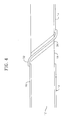
- the feed connection can be accomplished by connecting the microstrip line 16 to the conductive layer 14 near the slotline 18 with a jumper 32.
- the jumper 32 is fed through a slot 34 in the substrate 12. This feed provides better broadband characteristics, but is generally more difficult to fabricate.
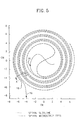
- the center slot spiral loops can be of reduced density, as shown in FIG. 5.
- This permits the possibility of exciting the microstrip feed at a point 36 within the periphery of the slot spiral.
- This feed geometry may be desirable for application having particular shape and space constraints.
- Another possibility is to offset the center of the spiral 22 while keeping the exterior of the spiral fixed, thus moving the microstrip/slotline transition point 22 to one side of center of the spiral. Doing so allows the direction of the radiation pattern of the antenna to be altered in a desired direction.
- each of the arms may be independently fed using the proposed infinite balun design in conjunction with the use of a hybrid device used for relative phase adjustment to satisfy pattern requirements.
- Other active or passive devices, such as amplifiers, etc., may be incorporated onto the same substrate 12.
- the slot spiral may be in any form (Archimedean, logarithmic ,rectangular, etc.) or combination of forms and may be any size, have any number of turns and growth rates.
- the number of arms in the spiral may also vary.
- the spiral may contain overlayed patterns such as zig-zaging, arm width modulation, etc., for size reduction and other advantages.
- the cavity may have absorbing or reflecting bottom and walls. It can include any combination of material fillings. It may be flat, conical or may be shaped in another manner.
- the inclusion of low loss substrates/superstrates in conjunction with the proposed slot spiral design is very desirable for antenna performance improvements and size reduction.
- filling the cavity 26 with the low loss material substrate 30 shifts the antenna operation to lower frequencies and is equivalent to reducing the antenna size.
- material layers (superstrates) 36 can be placed on the microstrip feed 16 side of the spiral for further size reduction and pattern control.
- the superstrate 36 may embody an air-pocket 38 around the microstrip line feed 16 or any other means to ensure that it does not alter the impedance of the feedline 16. Pattern control may be accomplished in connection with magnetic material and appropriate direct current bias.
- the superstrate 36 on the side of the microstrip feed 16 can be in the form of a dielectric lens 40 to yield higher gain and for additional pattern control, as shown in FIG. 7.
- the dielectric lens 40 acts to aim and focus the energy like a typical optical lens.
Landscapes
- Waveguide Aerials (AREA)
- Details Of Aerials (AREA)
Claims (20)
- Dispositif d'antenne en spirale à fente (10) comprenant :un substrat non conducteur (12) comportant des premier et second côtés ;une couche conductrice (14) sur ledit premier côté dudit substrat (12), ladite couche conductrice (14) comprenant une fente en forme de spirale (18) ; etcaractérisé en ce qu'un symétriseur et une source primaire intégrés sont une microbande (16) sur ledit second côté dudit substrat (12), ladite microbande (16) étant configurée pour s'enrouler vers le centre de ladite fente en forme de spirale (18) et pour réaliser une source primaire équilibrée par rapport à ladite fente en forme de spirale (18) au niveau d'un point de source primaire pour former un élément rayonnant.
- Dispositif d'antenne en spirale à fente (10) selon la revendication 1, comprenant, de plus :
une cavité réfléchissante peu profonde (26) comportant un support de cavité (28) configuré pour réfléchir le rayonnement émis par ledit élément rayonnant afin de rendre ledit élément de rayonnement unidirectionnel. - Dispositif d'antenne en spirale à fente (10) selon la revendication 2, dans lequel ladite cavité (26) est chargée par un matériau à fortes pertes (30).
- Dispositif d'antenne en spirale à fente (10) selon la revendication 2, dans lequel ladite cavité (26) est chargée par un matériau à faibles pertes (30).
- Dispositif d'antenne en spirale à fente (10) selon la revendication 2, dans lequel ledit support de cavité (28) est de forme non plane.
- Dispositif d'antenne en spirale à fente (10) selon la revendication 1, dans lequel ladite microbande (16) est configurée pour avoir une impédance égale à la moitié de l'impédance de ladite fente en forme de spirale (18) au niveau dudit point de source primaire.
- Dispositif d'antenne en spirale à fente (10) selon la revendication 5, dans lequel l'impédance de ladite microbande (16) est contrôlée en réduisant la largeur de la ligne de ladite microbande (16).
- Dispositif d'antenne en spirale à fente (10) selon la revendication 1, dans lequel ladite fente en forme de spirale (18) comprend, en outre des extrémités qui sont terminées pour empêcher les réflexions du signal.
- Dispositif d'antenne en spirale à fente (10) selon la revendication 8, comprenant, en outre un matériau à fortes pertes positionné à proximité desdites extrémités pour terminer lesdites extrémités.
- Dispositif d'antenne en spirale à fente (10) selon la revendication 1, dans lequel ladite couche conductrice (14) agit comme un plan de masse pour ladite microbande (16) et ladite source primaire équilibrée est réalisée en coupant ledit plan de masse en permettant à ladite microbande (16) de passer au-dessus de ladite ligne de fente (18) au niveau d'un point de source primaire au centre de ladite fente en forme de spirale (18), entraínant un couplage électromagnétique entre la microbande (16) et la ligne de fente (18), excitant la ligne de fente (18) sans contact entre la microbande (16) et la couche conductrice (14).
- Dispositif d'antenne en spirale à fente (10) selon la revendication 1, comprenant, en outre un cavalier conducteur (32) qui s'étend à travers une fente (34) dans ledit substrat (12), ledit cavalier (32) reliant ladite microbande (16) à une zone de ladite couche conductrice (14) à proximité de ladite fente en forme de spirale (18).
- Dispositif d'antenne en spirale à fente (10) selon la revendication 1, dans lequel ladite couche conductrice (14) agit comme un plan de masse pour ladite microbande (16) et ladite source primaire équilibrée est réalisée en coupant ledit plan de masse en permettant à ladite microbande (16) de passer au-dessus de ladite ligne de fente (18) au niveau d'un point de source primaire décalé par rapport au centre de ladite fente en forme de spirale (18), entraínant un couplage électromagnétique entre la microbande (16) et la ligne de fente (18), excitant la ligne de fente (18) sans contact entre la microbande (16) et la couche conductrice (14), dans lequel ladite direction de configuration de rayonnement peut être contrôlée par ledit décalage.
- Dispositif d'antenne en spirale à fente (10) selon la revendication 1, comprenant, en outre :
une couche supérieure (36) placée sur ledit second côté dudit substrat (12), ladite couche supérieure (36) étant un matériau à faibles pertes. - Dispositif d'antenne en spirale à fente (10) selon la revendication 4, comprenant, en outre :
une couche supérieure (36) placée du côté de ladite microbande (16) dudit substrat (12), ladite couche supérieure (36) présentant un plus grand contraste que ledit matériau à faibles pertes. - Dispositif d'antenne en spirale à fente (10) selon la revendication 14, comprenant, en outre :
des poches d'air (38) entourant ladite microbande (16), isolant ladite microbande (16) de ladite couche supérieure (36). - Dispositif d'antenne en spirale à fente (10) selon la revendication 13, dans lequel ladite couche supérieure (36) présente la forme d'une lentille (40) et est configurée pour diriger et focaliser le rayonnement produit par ledit dispositif d'antenne (10).
- Dispositif d'antenne en spirale à fente (10) selon la revendication 1, comprenant, en outre des moyens destinés à connecter ladite antenne à une source.
- Dispositif d'antenne en spirale à fente (10) selon la revendication 10, dans lequel ladite microbande (16) continue au-delà dudit point de source primaire pour réaliser une adaptation large bande.
- Dispositif d'antenne en spirale à fente (10) selon la revendication 18, dans lequel ladite microbande (16) continue au-delà dudit point de source primaire sur une distance égale à un multiple d'un quart de longueur d'onde d'une fréquence souhaitée pour le contrôle de bande passante.
- Dispositif d'antenne en spirale à fente (10) selon la revendication 18, dans lequel ladite microbande (16) est terminée par un matériau à fortes pertes.
Applications Claiming Priority (3)
| Application Number | Priority Date | Filing Date | Title |
|---|---|---|---|
| US584496 | 1996-01-11 | ||
| US08/584,496 US5815122A (en) | 1996-01-11 | 1996-01-11 | Slot spiral antenna with integrated balun and feed |
| PCT/US1996/020500 WO1997025755A1 (fr) | 1996-01-11 | 1996-12-23 | Antenne en spirale a fentes a source primaire et symetriseur integres |
Publications (2)
| Publication Number | Publication Date |
|---|---|
| EP0873577A1 EP0873577A1 (fr) | 1998-10-28 |
| EP0873577B1 true EP0873577B1 (fr) | 2000-05-03 |
Family
ID=24337556
Family Applications (1)
| Application Number | Title | Priority Date | Filing Date |
|---|---|---|---|
| EP96946132A Expired - Lifetime EP0873577B1 (fr) | 1996-01-11 | 1996-12-23 | Antenne en spirale a fentes a source primaire et symetriseur integres |
Country Status (6)
| Country | Link |
|---|---|
| US (1) | US5815122A (fr) |
| EP (1) | EP0873577B1 (fr) |
| AU (1) | AU2240297A (fr) |
| DE (1) | DE69608132T2 (fr) |
| ES (1) | ES2146428T3 (fr) |
| WO (1) | WO1997025755A1 (fr) |
Cited By (1)
| Publication number | Priority date | Publication date | Assignee | Title |
|---|---|---|---|---|
| CN105098340A (zh) * | 2015-07-18 | 2015-11-25 | 西安电子科技大学 | 一种小型化宽带螺旋天线 |
Families Citing this family (50)
| Publication number | Priority date | Publication date | Assignee | Title |
|---|---|---|---|---|
| GB2345798A (en) * | 1999-01-15 | 2000-07-19 | Marconi Electronic Syst Ltd | Broadband antennas |
| DE19904943B4 (de) * | 1999-02-06 | 2005-11-03 | Robert Bosch Gmbh | Spiralantenne |
| JP3440909B2 (ja) | 1999-02-23 | 2003-08-25 | 株式会社村田製作所 | 誘電体共振器、インダクタ、キャパシタ、誘電体フィルタ、発振器、誘電体デュプレクサおよび通信装置 |
| DE60037620T2 (de) | 1999-07-16 | 2008-12-24 | Mitsubishi Materials Corp. | Antennenanordnung |
| US6445354B1 (en) | 1999-08-16 | 2002-09-03 | Novatel, Inc. | Aperture coupled slot array antenna |
| US6422900B1 (en) | 1999-09-15 | 2002-07-23 | Hh Tower Group | Coaxial cable coupling device |
| US6404401B2 (en) * | 2000-04-28 | 2002-06-11 | Bae Systems Information And Electronic Systems Integration Inc. | Metamorphic parallel plate antenna |
| WO2002029928A2 (fr) * | 2000-10-02 | 2002-04-11 | Israel Aircraft Industries Ltd. | Antenne en spirale a fentes miniature |
| US6413103B1 (en) | 2000-11-28 | 2002-07-02 | Apple Computer, Inc. | Method and apparatus for grounding microcoaxial cables inside a portable computing device |
| US6437757B1 (en) | 2001-01-12 | 2002-08-20 | Lockheed Martin Corporation | Low profile antenna radome element with rib reinforcements |
| US6642898B2 (en) * | 2001-05-15 | 2003-11-04 | Raytheon Company | Fractal cross slot antenna |
| US6842157B2 (en) | 2001-07-23 | 2005-01-11 | Harris Corporation | Antenna arrays formed of spiral sub-array lattices |
| US6897829B2 (en) * | 2001-07-23 | 2005-05-24 | Harris Corporation | Phased array antenna providing gradual changes in beam steering and beam reconfiguration and related methods |
| US6466177B1 (en) | 2001-07-25 | 2002-10-15 | Novatel, Inc. | Controlled radiation pattern array antenna using spiral slot array elements |
| US20030114129A1 (en) * | 2001-12-17 | 2003-06-19 | Jerng Albert C. | System and method for a radio frequency receiver front end utilizing a balun to couple a low-noise amplifier to a mixer |
| US6781560B2 (en) * | 2002-01-30 | 2004-08-24 | Harris Corporation | Phased array antenna including archimedean spiral element array and related methods |
| US7075493B2 (en) * | 2002-05-01 | 2006-07-11 | The Regents Of The University Of Michigan | Slot antenna |
| US6897822B2 (en) * | 2002-06-03 | 2005-05-24 | The Johns Hopkins University | Spiral resonator-slot antenna |
| US6853351B1 (en) | 2002-12-19 | 2005-02-08 | Itt Manufacturing Enterprises, Inc. | Compact high-power reflective-cavity backed spiral antenna |
| US6885264B1 (en) | 2003-03-06 | 2005-04-26 | Raytheon Company | Meandered-line bandpass filter |
| US7429952B2 (en) * | 2005-12-23 | 2008-09-30 | Hemisphere Gps Inc. | Broadband aperture coupled GNSS microstrip patch antenna |
| US8131239B1 (en) | 2006-08-21 | 2012-03-06 | Vadum, Inc. | Method and apparatus for remote detection of radio-frequency devices |
| ATE513327T1 (de) * | 2007-12-18 | 2011-07-15 | Rohde & Schwarz | Antennenkoppler |
| US8810474B2 (en) * | 2008-11-11 | 2014-08-19 | Spectrum Control, Inc. | Antenna with high K backing material |
| US7986260B2 (en) * | 2009-02-18 | 2011-07-26 | Battelle Memorial Institute | Circularly polarized antennas for active holographic imaging through barriers |
| US20120181374A1 (en) | 2009-07-31 | 2012-07-19 | Lockheed Martin Corporation | Monopulse spiral mode antenna combining |
| US8193997B2 (en) * | 2009-08-20 | 2012-06-05 | Antennasys, Inc. | Directional planar log-spiral slot antenna |
| US9105972B2 (en) | 2009-08-20 | 2015-08-11 | Antennasys, Inc. | Directional planar spiral antenna |
| JP5471283B2 (ja) * | 2009-10-19 | 2014-04-16 | Tdk株式会社 | ワイヤレス給電装置、ワイヤレス受電装置およびワイヤレス電力伝送システム |
| US8390529B1 (en) * | 2010-06-24 | 2013-03-05 | Rockwell Collins, Inc. | PCB spiral antenna and feed network for ELINT applications |
| EP2403062A1 (fr) | 2010-06-30 | 2012-01-04 | BAE Systems PLC | Structure d'antenne |
| US9024840B2 (en) | 2010-06-30 | 2015-05-05 | Bae Systems Plc | Antenna structure |
| EP2589106B1 (fr) | 2010-06-30 | 2019-11-20 | BAE Systems PLC | Structure d'alimentation d'antenne |
| US8745853B2 (en) * | 2010-07-05 | 2014-06-10 | Universal Display Corporation | Antenna fabrication with three-dimensional contoured substrates |
| US8610515B2 (en) | 2011-05-09 | 2013-12-17 | Northrop Grumman Systems Corporation | True time delay circuits including archimedean spiral delay lines |
| RU2504055C1 (ru) * | 2012-08-10 | 2014-01-10 | Общество С Ограниченной Ответственностью Научно-Производственная Фирма "Электрон" | Щелевая полосковая антенна вытекающей волны с круговой поляризацией |
| WO2014078058A1 (fr) | 2012-11-15 | 2014-05-22 | 3M Innovative Properties Company | Antenne spirale pour systèmes de communications sans fil répartis |
| US9733353B1 (en) * | 2014-01-16 | 2017-08-15 | L-3 Communications Security And Detection Systems, Inc. | Offset feed antennas |
| US9821734B2 (en) * | 2015-03-13 | 2017-11-21 | Aero Advanced Paint Technology, Inc. | Concealed embedded circuitry, vehicles comprising the same, and related methods |
| US11088455B2 (en) | 2018-06-28 | 2021-08-10 | Taoglas Group Holdings Limited | Spiral wideband low frequency antenna |
| US11876297B2 (en) * | 2018-08-24 | 2024-01-16 | Kyocera Corporation | Structure, antenna, wireless communication module, and wireless communication device |
| WO2020249609A1 (fr) * | 2019-06-11 | 2020-12-17 | Gea Food Solutions Bakel B.V. | Dispositif de détection de température et moyen de transport |
| US10992046B2 (en) * | 2019-06-12 | 2021-04-27 | Bae Systems Information And Electronic Systems Integration Inc. | Low profile high gain dual polarization UHF/VHF antenna |
| CN110534892B (zh) * | 2019-09-23 | 2024-01-16 | 福州大学 | 一种小型化内侧螺旋耦合馈电的缝隙螺旋天线 |
| CN111082209B (zh) * | 2019-12-31 | 2021-09-21 | 上海微波技术研究所(中国电子科技集团公司第五十研究所) | 一种新型馈电方式的低剖面平面螺旋天线 |
| US11843166B2 (en) | 2020-12-09 | 2023-12-12 | Battelle Memorial Institute | Antenna assemblies and antenna systems |
| CN113161735B (zh) * | 2021-04-02 | 2024-05-17 | 福耀玻璃工业集团股份有限公司 | 一种应用于车载的定位天线及车辆玻璃 |
| CN113451778A (zh) * | 2021-05-14 | 2021-09-28 | 上海大学 | 加载螺旋型超构材料的小型化轻量化高效率微带贴片天线 |
| US12095497B2 (en) | 2021-05-26 | 2024-09-17 | Skyworks Solutions, Inc. | Signal conditioning circuits for coupling to antenna |
| US11799205B1 (en) | 2022-06-07 | 2023-10-24 | Honeywell Federal Manufacturing & Technologies, Llc | Spiral antenna assembly with integrated feed network structure and method of manufacture |
Family Cites Families (23)
| Publication number | Priority date | Publication date | Assignee | Title |
|---|---|---|---|---|
| US2863145A (en) * | 1955-10-19 | 1958-12-02 | Edwin M Turner | Spiral slot antenna |
| US2929064A (en) * | 1957-08-02 | 1960-03-15 | Hughes Aircraft Co | Pencil beam slot antenna |
| US2958081A (en) * | 1959-06-30 | 1960-10-25 | Univ Illinois | Unidirectional broadband antenna comprising modified balanced equiangular spiral |
| US3509465A (en) * | 1965-10-22 | 1970-04-28 | Sylvania Electric Prod | Printed circuit spiral antenna having amplifier and bias feed circuits integrated therein |
| US3633210A (en) * | 1967-05-26 | 1972-01-04 | Philco Ford Corp | Unbalanced conical spiral antenna |
| US3587106A (en) * | 1968-07-15 | 1971-06-22 | Gen Dynamics Corp | Broad band antennas having spiral windings |
| US3618114A (en) * | 1968-12-16 | 1971-11-02 | Univ Ohio State Res Found | Conical logarithmic-spiral antenna |
| US3760420A (en) * | 1969-09-22 | 1973-09-18 | Raytheon Co | Radiation seeker |
| GB2005083B (en) * | 1977-09-28 | 1982-05-19 | Secr Defence | Variable phase-shifters |
| US4161737A (en) * | 1977-10-03 | 1979-07-17 | Albright Eugene A | Helical antenna |
| US4319248A (en) * | 1980-01-14 | 1982-03-09 | American Electronic Laboratories, Inc. | Integrated spiral antenna-detector device |
| US4315266A (en) * | 1980-07-25 | 1982-02-09 | Nasa | Spiral slotted phased antenna array |
| JPS58123204A (ja) * | 1982-01-19 | 1983-07-22 | Mitsubishi Electric Corp | スパイラルアンテナ |
| US4525720A (en) * | 1982-10-15 | 1985-06-25 | The United States Of America As Represented By The Secretary Of The Navy | Integrated spiral antenna and printed circuit balun |
| US4559539A (en) * | 1983-07-18 | 1985-12-17 | American Electronic Laboratories, Inc. | Spiral antenna deformed to receive another antenna |
| US4630064A (en) * | 1983-09-30 | 1986-12-16 | The Boeing Company | Spiral antenna with selectable impedance |
| US4605934A (en) * | 1984-08-02 | 1986-08-12 | The Boeing Company | Broad band spiral antenna with tapered arm width modulation |
| US4823145A (en) * | 1986-09-12 | 1989-04-18 | University Patents, Inc. | Curved microstrip antennas |
| KR920002439B1 (ko) * | 1988-08-31 | 1992-03-24 | 삼성전자 주식회사 | 휴대용 무선전화기의 슬로트 안테나 장치 |
| GB2235590B (en) * | 1989-08-21 | 1994-05-25 | Radial Antenna Lab Ltd | Planar antenna |
| US5146234A (en) * | 1989-09-08 | 1992-09-08 | Ball Corporation | Dual polarized spiral antenna |
| KR960009447B1 (en) * | 1991-03-27 | 1996-07-19 | Lg Electronics Inc | A dipole array antenna |
| US5313216A (en) * | 1991-05-03 | 1994-05-17 | Georgia Tech Research Corporation | Multioctave microstrip antenna |
-
1996
- 1996-01-11 US US08/584,496 patent/US5815122A/en not_active Expired - Lifetime
- 1996-12-23 WO PCT/US1996/020500 patent/WO1997025755A1/fr not_active Ceased
- 1996-12-23 AU AU22402/97A patent/AU2240297A/en not_active Abandoned
- 1996-12-23 EP EP96946132A patent/EP0873577B1/fr not_active Expired - Lifetime
- 1996-12-23 DE DE69608132T patent/DE69608132T2/de not_active Expired - Fee Related
- 1996-12-23 ES ES96946132T patent/ES2146428T3/es not_active Expired - Lifetime
Cited By (1)
| Publication number | Priority date | Publication date | Assignee | Title |
|---|---|---|---|---|
| CN105098340A (zh) * | 2015-07-18 | 2015-11-25 | 西安电子科技大学 | 一种小型化宽带螺旋天线 |
Also Published As
| Publication number | Publication date |
|---|---|
| DE69608132T2 (de) | 2000-11-09 |
| DE69608132D1 (de) | 2000-06-08 |
| AU2240297A (en) | 1997-08-01 |
| US5815122A (en) | 1998-09-29 |
| WO1997025755A1 (fr) | 1997-07-17 |
| ES2146428T3 (es) | 2000-08-01 |
| EP0873577A1 (fr) | 1998-10-28 |
Similar Documents
| Publication | Publication Date | Title |
|---|---|---|
| EP0873577B1 (fr) | Antenne en spirale a fentes a source primaire et symetriseur integres | |
| US7245268B2 (en) | Quadrifilar helical antenna | |
| US5940036A (en) | Broadband circularly polarized dielectric resonator antenna | |
| US5539414A (en) | Folded dipole microstrip antenna | |
| US8487821B2 (en) | Methods and apparatus for a low reflectivity compensated antenna | |
| EP0406563A1 (fr) | Antenne à large bande à ligne d'alimentation à microbande | |
| US10978812B2 (en) | Single layer shared aperture dual band antenna | |
| JP3029231B2 (ja) | 二重円形偏波temモードのスロットアレーアンテナ | |
| US7855693B2 (en) | Wide band biconical antenna with a helical feed system | |
| US11881611B2 (en) | Differential fed dual polarized tightly coupled dielectric cavity radiator for electronically scanned array applications | |
| EP1033782B1 (fr) | Antenne monopole | |
| US7173576B2 (en) | Handset quadrifilar helical antenna mechanical structures | |
| WO2005094352A2 (fr) | Antenne multifaisceau | |
| EP2212970B1 (fr) | Antenne à double polarisation | |
| WO1998018177A1 (fr) | Antenne microruban superposee pour communication sans fil | |
| KR100198687B1 (ko) | 어레이 안테나 | |
| US6429824B2 (en) | Low profile, broadband, dual mode, modified notch antenna | |
| EP4205231B1 (fr) | Réseau d'antennes rf conforme et filtre de rejet eme hors bande intégré | |
| KR102172736B1 (ko) | T자형 슬롯을 이용한 광대역 원형편파 안테나 | |
| US20090033579A1 (en) | Circularly polarized horn antenna | |
| JP3002252B2 (ja) | 平面アンテナ | |
| JPH0629723A (ja) | 平面アンテナ | |
| US6011522A (en) | Conformal log-periodic antenna assembly | |
| JP2001358530A (ja) | 円偏波マイクロストリップアンテナ | |
| Eid et al. | An Octagon Antenna Array For Satellite Direct Broadcasting Reception During Moving |
Legal Events
| Date | Code | Title | Description |
|---|---|---|---|
| PUAI | Public reference made under article 153(3) epc to a published international application that has entered the european phase |
Free format text: ORIGINAL CODE: 0009012 |
|
| 17P | Request for examination filed |
Effective date: 19980807 |
|
| AK | Designated contracting states |
Kind code of ref document: A1 Designated state(s): DE ES FR GB IT NL |
|
| GRAG | Despatch of communication of intention to grant |
Free format text: ORIGINAL CODE: EPIDOS AGRA |
|
| 17Q | First examination report despatched |
Effective date: 19990820 |
|
| GRAG | Despatch of communication of intention to grant |
Free format text: ORIGINAL CODE: EPIDOS AGRA |
|
| GRAH | Despatch of communication of intention to grant a patent |
Free format text: ORIGINAL CODE: EPIDOS IGRA |
|
| GRAH | Despatch of communication of intention to grant a patent |
Free format text: ORIGINAL CODE: EPIDOS IGRA |
|
| GRAA | (expected) grant |
Free format text: ORIGINAL CODE: 0009210 |
|
| AK | Designated contracting states |
Kind code of ref document: B1 Designated state(s): DE ES FR GB IT NL |
|
| REF | Corresponds to: |
Ref document number: 69608132 Country of ref document: DE Date of ref document: 20000608 |
|
| ET | Fr: translation filed | ||
| ITF | It: translation for a ep patent filed | ||
| REG | Reference to a national code |
Ref country code: ES Ref legal event code: FG2A Ref document number: 2146428 Country of ref document: ES Kind code of ref document: T3 |
|
| PLBE | No opposition filed within time limit |
Free format text: ORIGINAL CODE: 0009261 |
|
| STAA | Information on the status of an ep patent application or granted ep patent |
Free format text: STATUS: NO OPPOSITION FILED WITHIN TIME LIMIT |
|
| 26N | No opposition filed | ||
| REG | Reference to a national code |
Ref country code: GB Ref legal event code: IF02 |
|
| PGFP | Annual fee paid to national office [announced via postgrant information from national office to epo] |
Ref country code: FR Payment date: 20021127 Year of fee payment: 7 |
|
| PGFP | Annual fee paid to national office [announced via postgrant information from national office to epo] |
Ref country code: NL Payment date: 20021128 Year of fee payment: 7 |
|
| PGFP | Annual fee paid to national office [announced via postgrant information from national office to epo] |
Ref country code: GB Payment date: 20021218 Year of fee payment: 7 |
|
| PGFP | Annual fee paid to national office [announced via postgrant information from national office to epo] |
Ref country code: DE Payment date: 20021230 Year of fee payment: 7 |
|
| PGFP | Annual fee paid to national office [announced via postgrant information from national office to epo] |
Ref country code: ES Payment date: 20030109 Year of fee payment: 7 |
|
| PG25 | Lapsed in a contracting state [announced via postgrant information from national office to epo] |
Ref country code: GB Free format text: LAPSE BECAUSE OF NON-PAYMENT OF DUE FEES Effective date: 20031223 |
|
| PG25 | Lapsed in a contracting state [announced via postgrant information from national office to epo] |
Ref country code: ES Free format text: LAPSE BECAUSE OF NON-PAYMENT OF DUE FEES Effective date: 20031224 |
|
| PG25 | Lapsed in a contracting state [announced via postgrant information from national office to epo] |
Ref country code: NL Free format text: LAPSE BECAUSE OF NON-PAYMENT OF DUE FEES Effective date: 20040701 Ref country code: DE Free format text: LAPSE BECAUSE OF NON-PAYMENT OF DUE FEES Effective date: 20040701 |
|
| GBPC | Gb: european patent ceased through non-payment of renewal fee |
Effective date: 20031223 |
|
| PG25 | Lapsed in a contracting state [announced via postgrant information from national office to epo] |
Ref country code: FR Free format text: LAPSE BECAUSE OF NON-PAYMENT OF DUE FEES Effective date: 20040831 |
|
| NLV4 | Nl: lapsed or anulled due to non-payment of the annual fee |
Effective date: 20040701 |
|
| REG | Reference to a national code |
Ref country code: FR Ref legal event code: ST |
|
| REG | Reference to a national code |
Ref country code: ES Ref legal event code: FD2A Effective date: 20031224 |
|
| PG25 | Lapsed in a contracting state [announced via postgrant information from national office to epo] |
Ref country code: IT Free format text: LAPSE BECAUSE OF NON-PAYMENT OF DUE FEES Effective date: 20051223 |