EP0874395A2 - Méthode et dispositif pour détecter la charge des structures sur un substrat dans un système de traitement au plasma - Google Patents
Méthode et dispositif pour détecter la charge des structures sur un substrat dans un système de traitement au plasma Download PDFInfo
- Publication number
- EP0874395A2 EP0874395A2 EP98303115A EP98303115A EP0874395A2 EP 0874395 A2 EP0874395 A2 EP 0874395A2 EP 98303115 A EP98303115 A EP 98303115A EP 98303115 A EP98303115 A EP 98303115A EP 0874395 A2 EP0874395 A2 EP 0874395A2
- Authority
- EP
- European Patent Office
- Prior art keywords
- workpiece
- charge
- layer
- recited
- sensor
- Prior art date
- Legal status (The legal status is an assumption and is not a legal conclusion. Google has not performed a legal analysis and makes no representation as to the accuracy of the status listed.)
- Withdrawn
Links
Images


Classifications
-
- H—ELECTRICITY
- H10—SEMICONDUCTOR DEVICES; ELECTRIC SOLID-STATE DEVICES NOT OTHERWISE PROVIDED FOR
- H10P—GENERIC PROCESSES OR APPARATUS FOR THE MANUFACTURE OR TREATMENT OF DEVICES COVERED BY CLASS H10
- H10P74/00—Testing or measuring during manufacture or treatment of wafers, substrates or devices
- H10P74/27—Structural arrangements therefor
- H10P74/277—Circuits for electrically characterising or monitoring manufacturing processes, e.g. circuits in tested chips or circuits in testing wafers
Definitions
- the present invention relates to plasma processing systems and, more particularly, to methods and apparatus for detecting pattern dependent charging of workpieces in a plasma processing system.
- electrical charging is a well known problem which can occur during the plasma processing of semiconductor devices leading to the degradation of the device performance.
- Electrical charging can, for example, be a problem when there are large antennas of conducting material such as metal or polysilicon attached to a transistor gate that utilizes a very thin (e.g., less than 100 angstroms) gate oxide. These antenna serve to collect a relatively high level of electrical charge by virtue of their large area. This electrical charge may then be funneled down onto a transistor (or other device) leading to performance degradation or outright destruction of the device.
- circuits In an effort to measure and/or characterize the charging that occurs during plasma processing, circuits have been developed to measure the resulting voltage potential (or a current flow) between a charge collection area on the surface of the semiconductor device wafer and the substrate of the semiconductor wafer. Circuits, such as these, are typically provided within the semiconductor wafer.
- United States Patent No. 5,315,145 describes a charge monitoring device using an EEPROM device that functions as a high impedance voltage sensor and/or current sensor with a memory capability.
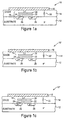
- Figures 1a-1c present cross-sectional views of a semiconductor wafer schematically depicting three different conventional charge monitoring devices.
- the semiconductor wafer includes a plurality of layers including a substrate 12 and an oxide layer 14.
- Each of the charge monitoring devices in Figures 1a, 1b and 1c includes an electrically programmable memory device having an Electrically Erasable and Programmable Read Only Memory (EEPROM) transistor 16 for measuring and/or characterizing the charge that accumulates on a charge collection electrode (CCE) 18 (e.g., located on the surface of the wafer) during plasma processing.
- EEPROM Electrically Erasable and Programmable Read Only Memory
- a voltage sensor 10 is depicted in Figure 1a.
- Voltage sensor 10 measures the positive potential between CCE 18 and substrate 12.
- Voltage sensor 10 includes EEPROM transistor 16 having a control electrode 20, a floating gate electrode 22, and source and drain regions 26.
- Control electrode 20 is connected to CCE 18.
- Floating electrode 22 is provided within oxide layer 14 and includes a projection 24 that extends towards source region 26.
- voltage sensor 10 includes a shunting diode 30 that is connected between CCE 18 and substrate 12. As depicted in Figure1a, diode 30 is connected to allow EEPROM transistor 16 to sense a positive potential between CCE 18 and substrate 12. If diode 30 is connected in the opposite direction between CCE 18 and substrate 12, as depicted by diode 30' in Figure 1b, then voltage sensor 10' measures the negative potential between CCE 18 and substrate 12.
- diode 30 (or 30') are not required.
- the EEPROM transistor 16 in the resulting voltage sensor is affected by both positive and negative electrical charging during the process.
- voltage sensor 10'' measures the voltage drop across resistor 32 as a result of the electrical charge accumulated on CCE 18 and the charge flux between CCE 18 and substrate 12.
- voltage sensor 10'' is essentially a charge flux sensor, or current sensor.
- V t1 threshold voltage associated with EEPROM transistor 16 is programmed prior to exposing the wafer to a process, such as a plasma process. Programming is typically accomplished by probing the wafer and supplying a programming signal to EEPROM transistor 16 via CCE 18.
- each EEPROM transistor 16 is again probed and a resulting threshold voltage (V t2 ) is measured.
- V t2 is typically accomplished by a parametric tester (not shown). This programming and measuring procedure is repeatable because each EEPROM transistor 16 is reprogrammable.
- Calibration curve 35 is a plot a threshold voltage V T versus a control gate voltage V G for an exemplary EEPROM transistor, where V T equals the difference in absolute magnitude between V t1 and V t2 .
- Calibration curve 35 depicts the substantially linear relationship between V T and V G .
- V G represents the potential between CCE 18 and substrate 12.
- voltage sensor 10 includes a known resistance, such as resistor 32 in Figure 1c, between CCE 18 and substrate 12, then the current that flowed through the resistor during plasma processing can be determined by applying Ohm s law (e.g., the current equals V G divided by the known resistance).
- Charge monitoring devices such as the prior art voltage and current sensors depicted in Figures 1a-c, are able to detect global wafer charging caused by non-uniformities in the plasma.
- the non-uniformities if significant enough, can lead to macroscopic level charging of the wafer.
- prior art charge monitoring devices are less effective in measuring charging occurring at the local microscopic level due to the topology of the fabricated device structure.
- Microscopic level charging can occur in a uniform plasma and is often dependent upon the pattern of the exposed surface of the wafer. For example, charging due to "electron shading", caused by the physical structure of the device is difficult to measure with the prior art charge monitoring devices.
- the methods and apparatus of the present invention are directed to creating electron shading that is measurable, such as, for example, on the charge collection electrode of a charge monitoring device.
- the topology of an exposed surface of a charge collection electrode is altered so as to more closely resemble the topology of the other devices/areas on the workpiece that are being processed in the plasma processing system.
- the measured electrical charge on the charge collection electrode, resulting during the plasma process includes additional charges due to electron shading. This measurement is more representative of the actual electrical charging on the other devices/areas of the workpiece, especially when compared to similar measurements made by the prior art charge monitoring devices.
- an apparatus for measuring an electrical charge deposited on a multiple-layered workpiece, such as a semiconductor wafer, during processing in a plasma processing system includes a charge collector, a patterned layer and a sensor.
- the charge collector is formed within one or more of the layers of the workpiece.
- the charge collector has a conducting surface on the workpiece.
- the patterned layer which is non-conducting, is provided on the conducting surface of the charge collector.
- the patterned layer creates a plurality of openings that extend through the patterned layer to the conducting surface of the charge collector.
- the sensor which is formed within one or more layers of the workpiece, is configured to sense an electrical charge of the charge collector.
- the patterned layer includes either a photoresist, a dielectric, a semiconductor, and/or an insulator material. Additionally, in accordance with certain embodiments, the openings in the patterned layer have an aspect ratio that cause a positive charge to accumulate on the conducting surface, during a plasma process, due at least in part to electron shading.
- the senor includes an electrically programmable memory device that is electrically programmable through the charge collector.
- an electrically programmable memory device in a voltage sensor and/or a current sensor.
- the apparatus includes at least two layers on the conducting surface of the charge collector, a contiguous layer and a non-conducting patterned layer which is on the contiguous layer
- a method for detecting pattern dependent charging on a workpiece during manufacture of the workpiece in a plasma processing system.
- the method includes forming a sensor that has a conducting surface and an electrically programmable memory device, covering at least a portion of the conducting surface with a patterned layer, subjecting the workpiece to a plasma in the plasma processing system, and measuring an electrical charge of the conducting surface with the electrically programmable memory device.
- the present invention is described with reference to etching processes, the methods and apparatus of the present invention are adaptable to other plasma processes, including CVD type processes, sputtering processes, and ion implantation processes.
- the first charging mechanism is essentially a global wafer charging mechanism that occurs due to non-uniformities in the plasma. This type of charging mechanism was described, for example, in S. Fang and J.P. McVittie, Proceedings of the International Reliability Physics Symposium, p. 13 (1993). This effect leads to macroscopic charging of the wafer and is readily detected by charge monitoring devices such as those depicted in Figures 1a-c, and those used in conventional CHARMTM wafers which are available from Wafer Charging Monitors, Inc. of Woodside, California.
- the second charging mechanism occurs in both uniform and non-uniform plasma and arises due to the charging of dielectric patterns, such as, for example, a photoresist layer, on the surface of the wafer. This effect occurs on a local microscopic level.
- This second mechanism has been referred to as "electron shading" and arises because of the difference in directionality of ions and electrons as they cross the plasma sheaf to the wafer. This mechanism has been described by Hashimoto, Jap. J Appl. Phys. 33 (part 1, no. 10), p. 6013 (1994).
- FIG. 3 schematically depicts electron shading on a semiconductor device.
- a top layer 40 of a device is shown formed over other device layers or over a substrate (not shown).
- a patterned photoresist layer 42 is provided on top layer 40.
- patterned photoresist layer 42 and top layer 40 are subjected to a plasma (that includes positively charged ions 44 and negatively charged electrons 46) which contacts patterned layer 42 and top layer 40 and results in a charge being deposited on either (or both) of patterned layer 42 and/or top lays 40.
- a plasma that includes positively charged ions 44 and negatively charged electrons 46
- the positive and negative charges have to become separated from one another.
- the charges will be separated by a structure, such as that shown in Figure 3, with a relative high aspect ratio (i.e., the ratio of the width of opening 48 to the depth of opening 48).
- a structure with a high aspect ratio is subjected to a plasma in a plasma processing system, positively charged ions are accelerated (e.g., as a result of a dc bias at the wafer), towards the wafer surface in a fairly directional manner as depicted by the arrows below ions 44.
- Electrons 46 are less affected by the dc bias and as such move in a more isotropic manner as depicted by the arrows around electrons 46. This results in an accumulation of positive charge at the bottom of opening 48 because, on average, positively charged ions 44 are more likely to penetrate to the bottom of opening 48 than are electrons 46. Thus, any structure with a high enough aspect ratio tends to charge more negatively at the top and more positively at the bottom. Hence, the term “electron shading" which describes the situation wherein the bottom of opening 48 is essentially shaded from electrons 46. This kind of charging mechanism is not readily detected by conventional charge monitoring devices such as those in the CHARMTM wafer, or in the prior art arrangements of Figure 1a-c.
- the methods and apparatus of the present invention are directed to creating electron shading on the charge collection electrode of a charge monitor, similar to the electron shading found on the other devices on the workpiece that are being fabricated via the plasma processing system.
- a modification is made to a CHARMTM wafer device (or similar charge monitoring device) to detect the additional electrical charging due to electron shading.
- the modification includes placing an appropriately patterned photoresist layer, or other type of non-conducting material layer, over CCE 18.
- the modification includes first placing a dielectric layer over CCE 18 and then placing an appropriately patterned photoresist layer, or other type of non-conducting material layer, over the dielectric layer
- the dielectric layer being selected to match or otherwise approximate the types of material(s) being affected by the plasma process.
- a layer of silicon dioxide can be used in monitoring a conductor (e.g., metal and/or polysilicon) etch plasma process, or a dielectric layer can be used in monitoring a dielectric(e.g., contact and/or via) etch application
- the patterned photoresist layer in the exemplary embodiments, forms openings that provide an appropriate aspect ratio to cause electron shading or to match other topologies of the workpiece.
- a patterned photoresist can comprise arrays of narrowly spaced, narrow lines, or small holes, depending upon the process and the topology of the device/structure that is being monitored and/or fabricated.
- FIG 4 depicts an improved charge monitoring device 100.
- Charge monitoring device 100 has many of the same design features as the devices of Figures 1a-c and like elements have the same reference numerals. However, charge monitoring device 100 is configurable as either a positive or negative voltage sensor (as depicted in Figures 1a and 1b, respectively) if element 34 is a properly connected diode (i.e., diode 30, or 30'). Charge monitoring device 100 is also configurable as a current sensor (as depicted in Figure 1c) if element 34 is a properly connected resistor (i.e., resistor 32).
- a non-contiguous patterned layer 102 is provided on an exposed surface 101 of CCE 18.
- Patterned layer 102 covers at least a portion of the exposed surface 101 and includes openings 104 that extend through patterned layer 102 to the exposed surface 101 of CCE 18.
- Patterned layer 102 includes at least one of a photoresist material, a dielectric material, a semiconductor material, and/or an insulator material.
- patterned layer 102 includes either a uniform or non-uniform array of lines 106 that are spaced apart so as to leave openings 104 in the space between the lines.
- patterned layer 104 resembles the type of pattern applied to other devices/areas being fabricated in the plasma processing system.
- each of the openings 104 includes an inherent aspect ratio, which is the ratio of the width of the opening to the depth of the opening.
- the aspect ratio is high enough to cause a positive charge to build up on CCE 18 during a plasma process due at least in part to the electron shading mechanism described above.
- charge monitoring device 100 measures the additional electrical charging due to electron shading.
- charge monitoring device 100 more accurately measures the charging as deposited on the other devices/areas that are being fabricated by providing a topology that more closely resembles the exposed topology of the devices/areas.
- One of the advantages of this improved charge measuring capability is improved control over the plasma process which tends to lead to a reduction in the damage to the wafer devices and lower manufacturing costs.
- FIG 5 depicts another embodiment of an improved charge monitoring device 100'.
- Charge monitoring device 100' has all of the same design features as the charge monitoring device 100 of Figures 4, and like elements have the same reference numerals.
- Charge monitoring device 100' is configurable as either a positive or negative voltage sensor (as depicted in Figures 1a and 1b, respectively) if element 34 is a properly connected diode (i.e., diode 30, or 30').
- Charge monitoring device 100' is also configurable as a current sensor (as depicted in Figure 1c) if element 34 is a properly connected resistor (i.e., resistor 32).
- a dielectric layer 110 is provided on CCE 18.
- Dielectric layer 110 is contiguous across exposed surface 101 of CCE 18.
- a patterned layer 102' is non-contiguous across dielectric layer 110 and includes openings 104'. Openings 104' extend through patterned layer 102' to reveal sections of dielectric layer 110 located above CCE 18.
- Charge monitoring device 100' is useful in monitoring or characterizing the charging that occurs during a plasma etching process wherein the topology of the wafer is altered during the process. For example, when a wafer containing a charge monitoring device 100' is subjected to an etching plasma, the molecules and atoms in the plasma etch through dielectric layer 102' via openings 104' to reveal the exposed surface 101 of CCE 18, assuming that conventional etching processing is properly performed. This etching changes the aspect ratio of openings 104' because the depth of openings 104' are increased as material from dielectric layer 110 is etched away. Thus, in this situation charge monitoring device 100' provides a more accurate measure of the charging occurring on the actual wafer devices/areas that are also being etched away during the plasma etching process.
- the embodiment of Figure 4 is useful in replicating the charging occurring elsewhere on the semiconductor wafer when, for example, an etching process is used to create contact holes, and/or vias.
- an etching process is used to create contact holes, and/or vias.
- dielectric layer 110 is an oxide which is to be etched
- a CF 4 process can be used to etch through dielectric layer 110 to CCE 18 during a contact or via etch process.
- the etching process could also etch a portion of CCE 18, providing that a sufficient portion of CCE 18 remains so as to be probed at a later stage in the manufacturing process.
- charge monitoring devices such as those in a CHARMTM wafer, more effectively measure the electrical charges that accumulate on other devises/areas within the wafer during a plasma process.
- One method to create such charge monitoring devices includes producing a charge monitoring device 10 (or 10', 10") having a CCE 18 and programming the EEPROM 16 (i.e., setting threshold voltage V t1 ) in charge monitoring device 10 in accordance with known principles, structures and methods.
- a photoresist layer is applied to the wafer such that an exposed surface 101 of CCE 18 is covered.
- the photoresist layer is then exposed with an appropriately configured mask and the exposed photoresist material is then developed out, thereby creating charge monitoring device 100 having a patterned layer 102 on exposed space 101.
- the wafer (and patterned layer 102) is exposed to a plasma process within a plasma processing system.
- patterned layer 102 is stripped off.
- patterned layer 102 is stripped off with a conventional wet process.
- EEPROM transistor 16 is probed and the threshold voltage (i.e., V t2 ) is measured.
- the method further includes providing a dielectric layer 110 between CCE 18 and a patterned layer 102' to create a charge monitoring device 100'.
- a method for detecting pattern dependent charging on a semiconductor wafer during manufacture and/or fabrication of a wafer in a plasma processing system includes providing a sensor (e.g., a charge monitor device 10 or 10', 10'') in the semiconductor wafer, the sensor having a conducting surface (e.g., a CCE 18), coupled to an electrically programmable memory device (e.g., EEPROM 16).
- the method includes covering at least a portion of the conducting surface with a patterned layer (e.g., patterned layer 102, or 110 and 102'), subjecting the wafer, including at least a portion of the conducting surface and the patterned layer to a plasma process in a plasma processing system.
- the method further includes measuring an accumulation of electrical charge on the exposed portion of the conducting surface and patterned layer with the electrically programmable memory device.
- Figure 6 illustrates the experimental results of processing a CHARMTM wafer in accordance with the above methods and apparatus in a LAM TCP 9600SE high density metal etch system, which is available from LAM Research Corporation of Fremont, California.
- Figure 6 shows the layout of the semiconductor water and a plot of data collected for an exemplary wafer which includes a plurality of dies each having a charge monitoring device.
- the layout of the water was such that about 25% of the charge monitoring devices had a patterned photoresist layer (of one-micron lines and spaces arranged in a checkerboard pattern) on their CCEs, the remaining charge monitoring devices had their CCEs completely covered with a non-patterned photoresist layer.
- the photoresist thickness was approximately 1.1 microns.
- the wafer was exposed to a non-etching argon plasma using approximately 400 watts TCP power at a pressure of about 20 mT and 100 sccm flow (with no wafer bias power applied) for approximately 60 seconds.
- the circled data represents the control gate voltages V G ) measured by the voltage sensors having the patterned photoresist layer on their CCEs, according to an embodiment of the present invention.
- the non-circled data represents the control gate voltages (V G ) measured by the voltage sensors having the non-patterned photoresist layer on their CCEs. It can be seen that the V G of the non-patterned photoresist covered sensors is about 1.7 volts, while the V G of the patterned photoresist covered sensors is higher, approximately 3.0 to 4.0 volts. Thus, the effects of electron shading of the charge collection electrode are apparent as measured by the differences in the measured V G .
Landscapes
- Testing Or Measuring Of Semiconductors Or The Like (AREA)
- Drying Of Semiconductors (AREA)
Applications Claiming Priority (2)
| Application Number | Priority Date | Filing Date | Title |
|---|---|---|---|
| US08/842,193 US5869877A (en) | 1997-04-23 | 1997-04-23 | Methods and apparatus for detecting pattern dependent charging on a workpiece in a plasma processing system |
| US842193 | 1997-04-23 |
Publications (2)
| Publication Number | Publication Date |
|---|---|
| EP0874395A2 true EP0874395A2 (fr) | 1998-10-28 |
| EP0874395A3 EP0874395A3 (fr) | 1999-05-26 |
Family
ID=25286743
Family Applications (1)
| Application Number | Title | Priority Date | Filing Date |
|---|---|---|---|
| EP98303115A Withdrawn EP0874395A3 (fr) | 1997-04-23 | 1998-04-22 | Méthode et dispositif pour détecter la charge des structures sur un substrat dans un système de traitement au plasma |
Country Status (2)
| Country | Link |
|---|---|
| US (1) | US5869877A (fr) |
| EP (1) | EP0874395A3 (fr) |
Cited By (3)
| Publication number | Priority date | Publication date | Assignee | Title |
|---|---|---|---|---|
| US6638833B1 (en) | 2001-03-09 | 2003-10-28 | Stmicroelectronics S.R.L. | Process for the fabrication of integrated devices with reduction of damage from plasma |
| EP1308997A3 (fr) * | 2001-11-06 | 2006-03-22 | Philips Intellectual Property & Standards GmbH | Dispositif semi-conducteur pour detecter des charges, système se composant d'un dispositif semi-conducteur pour détecter des charges, un dispositif semi-conducteur de référence, tranche, utlisation d'une tranche et méthode pour mesurer qualitativement le charge d'une tranche |
| CN104952847A (zh) * | 2014-03-28 | 2015-09-30 | 中芯国际集成电路制造(上海)有限公司 | 晶圆可接受测试结构及其形成方法 |
Families Citing this family (20)
| Publication number | Priority date | Publication date | Assignee | Title |
|---|---|---|---|---|
| JP3593825B2 (ja) * | 1996-11-08 | 2004-11-24 | ソニー株式会社 | 半導体装置及びその製造方法、並びに固体撮像素子の製造方法 |
| EP0848428B1 (fr) * | 1996-12-16 | 2003-04-23 | STMicroelectronics S.r.l. | Méthode d'évaluation des effets d'un traitement à plasma des puces semi-conducteurs |
| US6215129B1 (en) * | 1997-12-01 | 2001-04-10 | Vsli Technology, Inc. | Via alignment, etch completion, and critical dimension measurement method and structure |
| US6137119A (en) * | 1998-02-27 | 2000-10-24 | Micron Technology, Inc. | Apparatus for isolating a conductive region from a substrate during manufacture of an integrated circuit and connecting the conductive region to the substrate after manufacture |
| US6277691B1 (en) | 2000-04-04 | 2001-08-21 | Chartered Semiconductor Manufacturing Ltd. | Method to fabricate a robust and reliable memory device |
| US6544895B1 (en) * | 2000-08-17 | 2003-04-08 | Micron Technology, Inc. | Methods for use of pulsed voltage in a plasma reactor |
| US6485572B1 (en) * | 2000-08-28 | 2002-11-26 | Micron Technology, Inc. | Use of pulsed grounding source in a plasma reactor |
| US6741446B2 (en) * | 2001-03-30 | 2004-05-25 | Lam Research Corporation | Vacuum plasma processor and method of operating same |
| TW594455B (en) * | 2001-04-19 | 2004-06-21 | Onwafer Technologies Inc | Methods and apparatus for obtaining data for process operation, optimization, monitoring, and control |
| US6703641B2 (en) | 2001-11-16 | 2004-03-09 | International Business Machines Corporation | Structure for detecting charging effects in device processing |
| US6576922B1 (en) * | 2001-12-21 | 2003-06-10 | Texas Instruments Incorporated | Ferroelectric capacitor plasma charging monitor |
| US6830650B2 (en) * | 2002-07-12 | 2004-12-14 | Advanced Energy Industries, Inc. | Wafer probe for measuring plasma and surface characteristics in plasma processing environments |
| US6582977B1 (en) | 2002-08-29 | 2003-06-24 | Texas Instruments Incorporated | Methods for determining charging in semiconductor processing |
| US7470959B2 (en) * | 2003-11-04 | 2008-12-30 | International Business Machines Corporation | Integrated circuit structures for preventing charging damage |
| US20070296023A1 (en) * | 2006-06-21 | 2007-12-27 | Macronix International Co., Ltd. | Charge Monitoring Devices and Methods for Semiconductor Manufacturing |
| US20080083611A1 (en) * | 2006-10-06 | 2008-04-10 | Tegal Corporation | High-adhesive backside metallization |
| US8808513B2 (en) * | 2008-03-25 | 2014-08-19 | Oem Group, Inc | Stress adjustment in reactive sputtering |
| US8922227B2 (en) * | 2011-03-08 | 2014-12-30 | Freescale Semiconductor Inc. | Systems and methods for detecting surface charge |
| CN113497001B (zh) * | 2020-04-03 | 2024-03-29 | 长鑫存储技术有限公司 | 半导体结构 |
| CN113186501B (zh) * | 2021-03-17 | 2022-08-16 | 北京北方华创微电子装备有限公司 | 一种半导体设备 |
Family Cites Families (4)
| Publication number | Priority date | Publication date | Assignee | Title |
|---|---|---|---|---|
| US5315145A (en) * | 1993-07-16 | 1994-05-24 | Board Of Trustees Of The Leland Stanford Junior University | Charge monitoring device for use in semiconductor wafer fabrication for unipolar operation and charge monitoring |
| EP0678909B1 (fr) * | 1994-04-20 | 1999-07-14 | STMicroelectronics S.r.l. | Suivi d'une tension induite par un plasma RF sur un diélectrique de porte dans un appareil de gravure par plasma |
| US5548224A (en) * | 1995-01-20 | 1996-08-20 | Vlsi Technology, Inc | Method and apparatus for wafer level prediction of thin oxide reliability |
| US5594328A (en) * | 1995-02-14 | 1997-01-14 | Lukaszek; Wieslaw A. | Passive probe employing cluster of charge monitors for determining simultaneous charging characteristics of wafer environment inside IC process equipment |
-
1997
- 1997-04-23 US US08/842,193 patent/US5869877A/en not_active Expired - Lifetime
-
1998
- 1998-04-22 EP EP98303115A patent/EP0874395A3/fr not_active Withdrawn
Non-Patent Citations (1)
| Title |
|---|
| Collins Dictionary of the English Language, Second Edition, 1986, page 339 * |
Cited By (3)
| Publication number | Priority date | Publication date | Assignee | Title |
|---|---|---|---|---|
| US6638833B1 (en) | 2001-03-09 | 2003-10-28 | Stmicroelectronics S.R.L. | Process for the fabrication of integrated devices with reduction of damage from plasma |
| EP1308997A3 (fr) * | 2001-11-06 | 2006-03-22 | Philips Intellectual Property & Standards GmbH | Dispositif semi-conducteur pour detecter des charges, système se composant d'un dispositif semi-conducteur pour détecter des charges, un dispositif semi-conducteur de référence, tranche, utlisation d'une tranche et méthode pour mesurer qualitativement le charge d'une tranche |
| CN104952847A (zh) * | 2014-03-28 | 2015-09-30 | 中芯国际集成电路制造(上海)有限公司 | 晶圆可接受测试结构及其形成方法 |
Also Published As
| Publication number | Publication date |
|---|---|
| US5869877A (en) | 1999-02-09 |
| EP0874395A3 (fr) | 1999-05-26 |
Similar Documents
| Publication | Publication Date | Title |
|---|---|---|
| US5869877A (en) | Methods and apparatus for detecting pattern dependent charging on a workpiece in a plasma processing system | |
| US7105436B2 (en) | Method for in-line monitoring of via/contact holes etch process based on test structures in semiconductor wafer manufacturing | |
| EP0678909B1 (fr) | Suivi d'une tension induite par un plasma RF sur un diélectrique de porte dans un appareil de gravure par plasma | |
| US8241928B2 (en) | Test structure and method for detecting charge effects during semiconductor processing | |
| US8193824B2 (en) | Monitoring plasma induced damage during semiconductor wafer processes | |
| JP3250465B2 (ja) | 電子シェーディングダメージの測定方法 | |
| CN100593233C (zh) | 利用延迟反转点技术检测充电效应的测试结构与方法 | |
| US6790685B2 (en) | Method of forming a test pattern, method of measuring an etching characteristic using the same and a circuit for measuring the etching characteristic | |
| US6929965B2 (en) | Early response to plasma/charging damage by special pattern design of active region | |
| US7474001B2 (en) | Method for in-line monitoring of via/contact holes etch process based on test structures in semiconductor wafer manufacturing | |
| US5904490A (en) | Method of measuring electron shading damage | |
| US6143579A (en) | Efficient method for monitoring gate oxide damage related to plasma etch chamber processing history | |
| KR100448529B1 (ko) | 이온전류밀도 측정방법 및 측정장치 및 반도체디바이스제조방법 | |
| US6677766B2 (en) | Shallow trench isolation step height detection method | |
| US6362074B2 (en) | Integrated circuit processing with improved gate electrode fabrication | |
| US20030197175A1 (en) | Test structure for evaluating antenna effects | |
| US20070212800A1 (en) | Methods for detecting charge effects during semiconductor processing | |
| US6028005A (en) | Methods for reducing electric fields during the fabrication of integrated circuit devices | |
| JPWO2000055900A1 (ja) | イオン電流密度測定方法および測定装置並びに半導体デバイス製造方法 | |
| Choi et al. | A test structure for monitoring micro-loading effect of MOSFET gate length | |
| KR20090013881A (ko) | 테스트 웨이퍼, 그 제조 방법 및 이를 이용한 플라즈마데미지 측정 방법 | |
| KR100302600B1 (ko) | 반도체장치제조방법 | |
| US20040092044A1 (en) | Ion current density measuring method and instrument, and semiconductor device manufacturing method | |
| Patrick et al. | Study of pattern dependent charging in a high-density, inductively coupled metal etcher | |
| JP2002222926A (ja) | 半導体装置の製造方法及び半導体ウエハ |
Legal Events
| Date | Code | Title | Description |
|---|---|---|---|
| PUAI | Public reference made under article 153(3) epc to a published international application that has entered the european phase |
Free format text: ORIGINAL CODE: 0009012 |
|
| AK | Designated contracting states |
Kind code of ref document: A2 Designated state(s): DE FR GB IT |
|
| AX | Request for extension of the european patent |
Free format text: AL;LT;LV;MK;RO;SI |
|
| PUAL | Search report despatched |
Free format text: ORIGINAL CODE: 0009013 |
|
| AK | Designated contracting states |
Kind code of ref document: A3 Designated state(s): AT BE CH CY DE DK ES FI FR GB GR IE IT LI LU MC NL PT SE |
|
| AX | Request for extension of the european patent |
Free format text: AL;LT;LV;MK;RO;SI |
|
| 17P | Request for examination filed |
Effective date: 19990720 |
|
| AKX | Designation fees paid |
Free format text: DE FR GB IT |
|
| 17Q | First examination report despatched |
Effective date: 20030509 |
|
| STAA | Information on the status of an ep patent application or granted ep patent |
Free format text: STATUS: THE APPLICATION IS DEEMED TO BE WITHDRAWN |
|
| 18D | Application deemed to be withdrawn |
Effective date: 20031101 |