EP0876918B1 - Tête d'écriture électrostatique pour une machine d'impression électronique - Google Patents
Tête d'écriture électrostatique pour une machine d'impression électronique Download PDFInfo
- Publication number
- EP0876918B1 EP0876918B1 EP98106393A EP98106393A EP0876918B1 EP 0876918 B1 EP0876918 B1 EP 0876918B1 EP 98106393 A EP98106393 A EP 98106393A EP 98106393 A EP98106393 A EP 98106393A EP 0876918 B1 EP0876918 B1 EP 0876918B1
- Authority
- EP
- European Patent Office
- Prior art keywords
- dielectric
- control
- printing press
- electrode
- electrostatic printing
- Prior art date
- Legal status (The legal status is an assumption and is not a legal conclusion. Google has not performed a legal analysis and makes no representation as to the accuracy of the status listed.)
- Expired - Lifetime
Links
- 239000011248 coating agent Substances 0.000 claims 1
- 238000000576 coating method Methods 0.000 claims 1
- 210000002381 plasma Anatomy 0.000 description 32
- 150000002500 ions Chemical class 0.000 description 8
- 238000010276 construction Methods 0.000 description 7
- 239000003989 dielectric material Substances 0.000 description 7
- 239000003990 capacitor Substances 0.000 description 6
- 239000007789 gas Substances 0.000 description 6
- 239000000758 substrate Substances 0.000 description 6
- 239000002800 charge carrier Substances 0.000 description 4
- 230000001681 protective effect Effects 0.000 description 4
- 230000015572 biosynthetic process Effects 0.000 description 3
- 239000000919 ceramic Substances 0.000 description 3
- 238000000034 method Methods 0.000 description 3
- XKRFYHLGVUSROY-UHFFFAOYSA-N Argon Chemical compound [Ar] XKRFYHLGVUSROY-UHFFFAOYSA-N 0.000 description 2
- IJGRMHOSHXDMSA-UHFFFAOYSA-N Atomic nitrogen Chemical compound N#N IJGRMHOSHXDMSA-UHFFFAOYSA-N 0.000 description 2
- 238000009826 distribution Methods 0.000 description 2
- 230000000694 effects Effects 0.000 description 2
- 230000005684 electric field Effects 0.000 description 2
- 229910018072 Al 2 O 3 Inorganic materials 0.000 description 1
- 239000004642 Polyimide Substances 0.000 description 1
- 229910004298 SiO 2 Inorganic materials 0.000 description 1
- 238000000137 annealing Methods 0.000 description 1
- 229910052786 argon Inorganic materials 0.000 description 1
- 238000000889 atomisation Methods 0.000 description 1
- 238000006243 chemical reaction Methods 0.000 description 1
- 239000003086 colorant Substances 0.000 description 1
- 238000006880 cross-coupling reaction Methods 0.000 description 1
- 230000003292 diminished effect Effects 0.000 description 1
- 238000010891 electric arc Methods 0.000 description 1
- 230000003628 erosive effect Effects 0.000 description 1
- 230000008020 evaporation Effects 0.000 description 1
- 238000001704 evaporation Methods 0.000 description 1
- 239000011521 glass Substances 0.000 description 1
- 208000037824 growth disorder Diseases 0.000 description 1
- 238000010030 laminating Methods 0.000 description 1
- 239000007788 liquid Substances 0.000 description 1
- 239000000463 material Substances 0.000 description 1
- 239000010445 mica Substances 0.000 description 1
- 229910052618 mica group Inorganic materials 0.000 description 1
- 239000000203 mixture Substances 0.000 description 1
- 229910052757 nitrogen Inorganic materials 0.000 description 1
- 210000000056 organ Anatomy 0.000 description 1
- 230000003071 parasitic effect Effects 0.000 description 1
- 229920001721 polyimide Polymers 0.000 description 1
- 230000002123 temporal effect Effects 0.000 description 1
Images


Classifications
-
- B—PERFORMING OPERATIONS; TRANSPORTING
- B41—PRINTING; LINING MACHINES; TYPEWRITERS; STAMPS
- B41J—TYPEWRITERS; SELECTIVE PRINTING MECHANISMS, i.e. MECHANISMS PRINTING OTHERWISE THAN FROM A FORME; CORRECTION OF TYPOGRAPHICAL ERRORS
- B41J2/00—Typewriters or selective printing mechanisms characterised by the printing or marking process for which they are designed
- B41J2/385—Typewriters or selective printing mechanisms characterised by the printing or marking process for which they are designed characterised by selective supply of electric current or selective application of magnetism to a printing or impression-transfer material
- B41J2/39—Typewriters or selective printing mechanisms characterised by the printing or marking process for which they are designed characterised by selective supply of electric current or selective application of magnetism to a printing or impression-transfer material using multi-stylus heads
- B41J2/395—Structure of multi-stylus heads
Definitions
- the present invention relates generally to miniature loaders for application a controlled amount of electrical charge on a receptor.
- the invention relates to a write head for an electronic printing machine.
- Some charging devices use corona discharge or arc discharge applied to generate charge carriers. Such devices suffer from one locally very specific and sporadic electron leakage from a cathode, what that Controlling the charging process difficult. It is also difficult to have a high plasma space loading density maintain and thus the possible cathode current density reduce.
- the charge carriers are in a direct current annealing plasma generated. Although such devices are denser, more conductive Creating plasma as corona devices, it is a disadvantage that the cathode Plasma still needs to be exposed. Due to the nature of the surface Functional fluctuations and edge effects occur on the cathode surface, uneven current distributions and electric fields appear. This uneven current distributions and electrical fields cause one time-related fluctuation pattern of "hot spots" on the cathode surface, what generally by atomization and "hot spots” glow-electric evaporation leads to rapid erosion. Furthermore, in the plasma generated chemically reactive types of charge carriers (especially if that Plasma is generated in air) decompose the electrode exposed to the plasma or oxidize. These effects can significantly affect the life of such a device shorten. In addition, these devices require the formation of the appropriate one Plasmas an environment containing a gas and a complicated, controlled one Gas supply system.
- High frequency discharge is used in other charging devices.
- the Strength of the transferred charge is controlled by the length of time that the Discharge ignited, controlled as described in US 4,992,807. This has the disadvantage that the high-frequency source must be given pulses and thus the plasma is repeatedly ignited and cooled.
- Toshiba Corporation also has an "ion-jet" printhead described, in which on both sides of a ceramic layer two electrodes in Connection with an alternating voltage lead can be used.
- this printhead is used to apply large amounts of charge, it is not Print head and can therefore not be individual, corresponding to a picture element Apply loads.
- a separate control electrode is required on the side of the ceramic layer, and directly on the No control electrode is provided in the ceramic layer.
- EP-A-0 541 841 discloses an electrostatic printing machine according to the preamble of claim 1.
- charge carriers are caused by a high-frequency gas discharge generated.
- the electrode that sends the radio frequency signal is on one One side of a dielectric body is arranged, and the discharge is on a second one Side ignited.
- the high-frequency electrode is therefore not exposed to the plasma.
- a control electrode is provided on the second side of the dielectric body causes a controlled amount of electrical charge to the receptor, e.g. B. one Printing cylinder in a printing press, is transferred.
- a high frequency source is applied to a High-frequency electrode applied to generate a plasma on a first Side of the dielectric body is arranged.
- a variety of control electrodes are arranged on the second side of the dielectric body and ensure that correct loads.
- the voltage at the high-frequency electrode is sufficiently high, it ignites near the second side of the dielectric body a plasma, the electron, negative contains charged ions and positively charged ions.
- the plasma control signals are sent to the plurality of control electrodes.
- the average voltage of the plasma in the vicinity of the control electrode changes by the value of the control signal, but the state of the plasma remains basically unaffected with regard to its earth potential.
- the receptor is e.g. B. a printing cylinder with a dielectric layer, which are on a grounded layer or on a charged with a constant voltage Layer supports. The charging of the receptor continues until it is on Potential that is equal to the potential of the control electrode is charged. To At this point, the ions in the plasma will no longer go towards the receptor dressed.
- the device of the present invention can because of the excellent Plasma formation, which is achieved by the high-frequency electrode, advantageously and preferably used in ordinary atmospheric pressure environments become.
- the device is also for operation in an atmosphere that is gas (e.g. argon, nitrogen or gas-air mixtures), the supply of which is controlled, suitable.
- gas e.g. argon, nitrogen or gas-air mixtures
- the use of ordinary atmospheric air simplifies use of the print head is essential, whereas a controlled gas atmosphere, which is suitable for some prior art devices are needed, a complicated one Gas supply system required and also to crosstalk between the control electrodes arranged side by side leads. This crosstalk is in ordinary atmospheric environment diminished or almost eliminated because the average free range of plasma ions is quite short.
- the loading devices are advantageously, but not necessarily, arranged in a row side by side.
- An arrangement of these devices can be used as an electrostatic write head with a printing press. With such use, the receptor would be the surface of a cylinder of the printing press. With such an arrangement of charging devices, pixels are written on the printing cylinder, which have a grid spacing of approximately 50 ⁇ m and a charging current density of approximately 1 mA / cm 2 and are suitable for fast electrostatic writing, with a gray scale at a speed in the range of approx. 1 m / s.
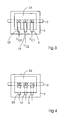
- Fig. 1 shows a side view along the length of an embodiment of the present invention, in which a continuous, sinusoidal High frequency source 1 from 800 to 3000 volts from peak to peak at 4 kHz to 1 MHz is applied to a high-frequency electrode 2. Except for contact with the High-frequency source 1, the electrode 2 is encased and supported by a suitable one dielectric medium or an insulating substrate (not shown) or on top of it built to prevent parasitic electronic discharges from the electrode.
- the high-frequency electrode 2 is along a first side 3 of a dielectric Body 4 of usually 10 microns to 100 microns thick arranged.
- the electrode 2 Preferably extends the electrode 2 extends along the entire width of the dielectric body 4.
- One Control electrode 5, for example 10 microns to 50 microns wide and one of a Variety of control electrodes is on the second side 6 of the dielectric Body 4 arranged.
- the control electrode 5 is capacitively grounded. Here is this Grounding through the capacitor 8 is shown schematically, for example with a Capacitance from 3 to 100 pF.
- a resistor 7, the z. B. a resistance value of 1 mega-ohm can be used to provide a control signal source 10 To protect against current surges.
- the control electrode 5 is positioned so that a Overlap is just avoided or so that this is the horizontal position of the High-frequency electrode 2 overlapped more or less.
- the dielectric body 4 should be free of pinholes and resistant to the formation of pinholes during operation. Puncture holes in the dielectric body 4 can cause a strong direct current to flow through the dielectric body, which disrupts the control mechanism and causes physical damage in the area of the puncture holes.
- the dielectric body 4 can have several layers of dielectric material because the layer construction prevents growth disorders from spreading through the entire thickness of the dielectric body 4. A natural mica, 30 ⁇ m thick and of course comprising several layers, has shown excellent durability, even if the atmosphere used for the plasma was air.
- An artificial dielectric body 4 with one or more layers of dielectric material can be created by layering or laminating the same dielectric material or by alternating layers of different materials. Such dielectric materials can include KAPTAN-PR, a polyimide manufactured by DuPont, glass, and other common dielectric films such as. B. SiO 2 or Al 2 O 3 .
- the high-frequency electrode 2 preferably works at 4 kHz to 400 kHz or above; at this frequency a stable plasma is formed, that can tolerate fluctuating control voltages.
- a control signal 10 is issued while this state of the plasma is being maintained in the range of -600 V to +600 V to the control electrode 5.
- the DC voltage via the dielectric body 4 in the vicinity of the control electrode 5 changes by the value of the voltage generated by the control signal source 10, however apart from its earth potential, the state of the plasma 9 remains unaffected. Consequently when the control signal 10 is applied, the appearance of the plasma 9 (in its size, color, brightness, etc.) little.
- the ground connections of the high-frequency source 1 and the control signal source 10 are connected to the Ground connection of a conductive reference electrode 11 (for example a grounded layer) a receptor 12, the surface 13 of which must be charged, connected. This is true e.g. B. towards a printing cylinder surface. If the receptor 12 is close to the plasma 9 comes up, the surface 13 is charged to a potential that the Voltage potential at the control electrode 5 corresponds. Under normal Operating conditions fluctuate the actual potential of the receptor surface 13 in an almost linear relationship to that applied to the control electrode 5 Voltage, but offset by an offset voltage.
- the offset voltage for a particular system is 30 volts and then a voltage of minus 30 volts is applied by the control signal source 10 surface 13 is charged up to a zero potential or earth potential. If a voltage of 70 volts is applied by the control signal source 10, then the Surface 13 charged to a potential of approximately 100 volts.
- the difference or Offset voltage between the voltage of the control signal source 10 and that at the Surface 13 applied potential is advantageously within a Voltage range of +/- 300 volts pretty constant.
- the offset voltage can be used for a certain construction, e.g. B. a printing press, measured and for calculation the desired control signal voltages that are required for a desired potential at the Surface 13 must be created, are used. If the offset voltage is constant, this calculation is a simple step of addition or subtraction.
- the charging device of the present invention thus enables accurate Process of applying a charge to a receptor over a wide range of tensions.
- FIG. 7 schematically shows a system for calculating the charging current, I OUT , of the charging device of FIG. 1, in which the charging current is applied to a surface from a specific distance d (as shown).
- This system can also be used to calculate the offset voltage described above.
- a test electrode 111 is connected to a screen 115, on which the charging current is then displayed, namely through the resistance element 117, which, for. B. has a resistance of 100 kilohms.
- a capacitor 118 with a low capacitance, for example with a capacitance of 0.1 microfarads, can also be connected in the manner shown. Since the control voltage V c , which is grounded and coupled to a capacitor 119 (e.g.
- the charging current is measured by the oscillograph .
- the width of the test electrode (as shown in FIG. 7) can be expanded to a width that equals a pixel width multiplied by a factor m, where a single control voltage is applied to a plurality of control electrodes.
- the charging current for an individual control electrode, the width of which is equal to a pixel width, can then be calculated by dividing the measured charging current by the factor m.
- the charging current fluctuates from a distance d of 0.25 mm almost linear with the voltage applied to the control electrode 5.
- the charging current is approximately zero, which is equivalent to the fact that no charge is applied to the receptor surface. It is charging current of higher values is also available if the distance d is reduced and / or the high-frequency voltage is increased.
- Other options, such as B. measuring the actual charge or Potential applied to the receptor surface and measuring its surface temporal reactions are equally valid.
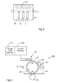
- the loading devices of the present invention for use as a write head 100 in a printing press are advantageously arranged in a side-by-side row.
- a plurality of control electrodes 5, 15 and 25 are arranged on the second side 6 of a single dielectric body 4.
- Each of the control electrodes 5, 15, 25, etc. has an independent control signal V C1 , V C2 , V C3 , etc.
- the end faces of the control electrodes 5, 15, 25 are typically oriented at an angle of 90 ° with respect to the high-frequency electrode 2. In such an arrangement of the charging devices, crosstalk between the control electrodes 5, 15, and 25 can be reduced by installing insulating structures.
- control electrodes can be coated with a layer of dielectric Material are coated, only the ends of the control electrodes, which the Nearest plasma are left uncoated.
- the process in Atmospheric air takes place as is preferred, be such insulating Constructions are hardly necessary.
- an insulating structure 24 is provided with an open end to To reduce cross-coupling between the control electrodes 5, 15 and 25.
- This Open ended insulating structure 24 can be made from a ribbed cover dielectric material. You can also be a senior contractor or a Protective electrode, the z. B. is connected to a constantly charged source and Scattered ions are absorbed or "scooped up" or hold the ion flow.
- Fig. 4 is another embodiment in which an insulating or conductive Construction 26 is provided with a closed end.
- This isolating Construction 26 can also be a ribbed cover made of dielectric material or be a pickup or a protective electrode.
- a transducer or a Protective electrode 27 at the opposite ends of the Control electrodes 5, 15, 25 may be placed to reduce crosstalk.
- the write head 100 of the present invention is as a component of a electrostatic printing machine 200 shown.
- a mass storage device 210 can do that Save data representing the image to be printed, including the gray scale data.
- the Processor 205 provides the correct voltage for each control electrode of the Printhead 100 according to the data representing the image to be printed.
- On Pressure organ, d. H. an impression cylinder 26 has a dielectric surface 27 which serves as a receptor.
- the dielectric surface 27 is on a conductive Layer 28, which serves as a conductive reference electrode and a grounded layer or a layer set by a controller to a certain constant voltage can be.
- the write head 100 is in the vicinity of the dielectric surface 27 of the Printing cylinder 26 arranged, and the individual control electrodes extend along the length of the write head 100.
- the write head 100 is similar to that in FIG. 2 shown type, however, the write head in Fig. 2 is reversed, so that the plasma 9th contacts the dielectric surface 27.
- the pressure cylinder 26 rotates in the direction indicated; the moves dielectric surface 27 of the printing cylinder 26 close to the write head 100.
- the Control processor 205 sends control signals to the plurality of control electrodes which are contained in the write head 100 in order to achieve the charged pixels on the dielectric surface 27 of the printing cylinder 26 to record so that a latent image arises.
- a color source 32 In Fig. 6, this color source 32 consists of two Ink rollers that are connected to an ink fountain, however, can also be any other color source can be used. Color, as it is to be defined here, exists both from liquid colors and from dry toner.
- a Printing substrate 34 e.g. B. a paper web or a sheet of paper in contact.
- the Print substrate 34 may be in contact with dielectric surface 27 through a Impression cylinder 35 are held in a suitable position. At the contact point transfer the color to the printing substrate 34 and thus the image 36 to the Print substrate 34 printed.
- the dielectric surface 27 then passes through one Extinguishing device 37, e.g. B. a source of ultraviolet light.
- the present invention also applies to copying machines and Fax machines that are here under the definition of electrostatic printing presses included, can be used.
- the invention is also for a four-color printing press usable, in which each of four printing cylinders one Has printhead and the four printheads by a common Control processor can be controlled.
Landscapes
- Printers Or Recording Devices Using Electromagnetic And Radiation Means (AREA)
- Electrophotography Using Other Than Carlson'S Method (AREA)
Claims (8)
- Machine à imprimer électrostatique,caractériséecomprenant un organe d'impression (26) qui possède une surface diélectrique (13, 27), comprenant en outre une tête d'écriture (100) destinée à déposer électriquement des charges sur la surface diélectrique (13,27), un corps diélectrique (4) qui présente un premier côté (3) et un deuxième côté (6), une électrode à haute fréquence (2) qui est disposée sur la premier côté (3) du corps diélectrique (4) et est appropriée pour recevoir un signal à haute fréquence d'une source de haute fréquence (1) de manière qu'il s'établisse un plasma (9) à proximité du deuxième côté (6) du corps diélectrique (4), et une pluralité d'électrodes de commande (5, 15, 25) qui sont disposées sur le deuxième côté (6) du corps diélectrique (4) et sont appropriées pour recevoir des signaux de commande du source de signaux de commande (10),et comprenant un processeur de commande(205) qui est relié à la pluralité d'électrodes de commande (5, 15, 25) pour les commander individuellement,qui est reliée aux connexions de terre de la source de haute fréquence (1) et à la source de signaux de commande (10), de sorte qu'au moins une électrode de commande (5) entre en contact électrique avec la surface diélectrique (13, 27) à travers le plasma (9).en ce que l'électrode à haute fréquence (2) s'étend sur toute la largeur du corps diélectrique (4),et en ce que l'organe d'impression (12, 26) présente sous sa surface diélectrique (13, 27) une couche conductrice et mise à la terre (11, 28),
- Machine à imprimer électrostatique selon la revendication 1,
caractérisée, en ce qu'il est prévu en supplément une source d'encre (32) à partir de laquelle de l'encre est mise en contact avec la surface diélectrique (27) de l'organe d'impression (26). - Machine à imprimer électrostatique selon la revendication 1,
caractérisée en ce qu'un revêtement diélectrique est déposé sur au moins une de la pluralité d'électrodes de commande (5, 15, 25), - Machine à imprimer électrostatique selon la revendication 1,
caractérisée en ce que le signal à haute fréquence est continuel. - Machine à imprimer électrostatique selon la revendication 1,
caractérisée en ce qu'il est prévu une construction isolante (24) par laquelle une diaphonie entre les électrodes de commande (5, 15, 25) est réduite. - Machine à imprimer électrostatique selon la revendication 5,
caractérisée en ce que la construction isolante (24) est un extracteur ou une électrode de protection. - Machine à imprimer électrostatique selon la revendication 5,
caractérisée en ce que la construction isolante (24) et un capot diélectrique nervuré. - Machine à imprimer électrostatique selon la revendication 1,
caractérisée en ce que l'organe d'impression (26) est un cylindre d'impression.
Applications Claiming Priority (2)
| Application Number | Priority Date | Filing Date | Title |
|---|---|---|---|
| US852970 | 1992-03-17 | ||
| US08/852,970 US6160567A (en) | 1997-05-08 | 1997-05-08 | Electrostatic write head for electronic printing press |
Publications (3)
| Publication Number | Publication Date |
|---|---|
| EP0876918A2 EP0876918A2 (fr) | 1998-11-11 |
| EP0876918A3 EP0876918A3 (fr) | 1999-08-04 |
| EP0876918B1 true EP0876918B1 (fr) | 2001-11-28 |
Family
ID=25314684
Family Applications (1)
| Application Number | Title | Priority Date | Filing Date |
|---|---|---|---|
| EP98106393A Expired - Lifetime EP0876918B1 (fr) | 1997-05-08 | 1998-04-08 | Tête d'écriture électrostatique pour une machine d'impression électronique |
Country Status (4)
| Country | Link |
|---|---|
| US (1) | US6160567A (fr) |
| EP (1) | EP0876918B1 (fr) |
| JP (1) | JPH10315530A (fr) |
| DE (2) | DE19815793A1 (fr) |
Families Citing this family (4)
| Publication number | Priority date | Publication date | Assignee | Title |
|---|---|---|---|---|
| DE10030171A1 (de) * | 2000-06-20 | 2002-01-03 | Heidelberger Druckmasch Ag | Vorrichtung zum Aufzeichnen eines elektrostatischen Musters auf einen Bildträger und Verfahren zum Betreiben der Aufzeichnungsvorrichtung |
| ATE459375T1 (de) * | 2005-12-09 | 2010-03-15 | Basf Se | Copolymere auf basis von polyalkylenoxid- modifizierten n-vinyllactam-copolymeren |
| US20080100534A1 (en) * | 2006-10-26 | 2008-05-01 | Hewlett-Packard Development Company Lp | Switch |
| WO2009040248A1 (fr) * | 2007-09-27 | 2009-04-02 | Basf Se | Agents améliorant la systémicité |
Family Cites Families (10)
| Publication number | Priority date | Publication date | Assignee | Title |
|---|---|---|---|---|
| US4792860A (en) * | 1987-02-27 | 1988-12-20 | Kuehrle Manfred R | Thermodynamic printing method and means |
| US4841313A (en) * | 1987-06-16 | 1989-06-20 | Delphax Systems | RF driver and control |
| US4992807A (en) * | 1990-05-04 | 1991-02-12 | Delphax Systems | Gray scale printhead system |
| US5159358A (en) * | 1991-06-19 | 1992-10-27 | Delphax Systems | Divided screen printer |
| US5270729A (en) * | 1991-06-21 | 1993-12-14 | Xerox Corporation | Ionographic beam positioning and crosstalk correction using grey levels |
| JP2937577B2 (ja) * | 1991-09-11 | 1999-08-23 | 双葉電子工業 株式会社 | 蛍光プリンタ用光源 |
| EP0541841A1 (fr) * | 1991-11-12 | 1993-05-19 | Moore Business Forms, Inc. | Méthode et appareil pour la formation d'images électrostatiques |
| IL103705A (en) * | 1991-11-15 | 1995-12-08 | Kuehnle Manfred R | Electro-thermal printing ink and method and printing device with its help |
| DE4413237A1 (de) * | 1994-04-15 | 1995-10-19 | Heidelberger Druckmasch Ag | Schreibeinrichtung zum gesteuerten Aufbringen von Ladungsträgern auf ein Substrat |
| EP0706891A3 (fr) * | 1994-10-13 | 1998-05-06 | Imagine Ltd. | Appareil et procédés pour l'impression numérique sans impact |
-
1997
- 1997-05-08 US US08/852,970 patent/US6160567A/en not_active Expired - Fee Related
-
1998
- 1998-04-08 DE DE19815793A patent/DE19815793A1/de not_active Withdrawn
- 1998-04-08 DE DE59802198T patent/DE59802198D1/de not_active Expired - Fee Related
- 1998-04-08 EP EP98106393A patent/EP0876918B1/fr not_active Expired - Lifetime
- 1998-05-07 JP JP10124684A patent/JPH10315530A/ja active Pending
Also Published As
| Publication number | Publication date |
|---|---|
| EP0876918A3 (fr) | 1999-08-04 |
| EP0876918A2 (fr) | 1998-11-11 |
| DE19815793A1 (de) | 1998-11-12 |
| DE59802198D1 (de) | 2002-01-10 |
| JPH10315530A (ja) | 1998-12-02 |
| US6160567A (en) | 2000-12-12 |
Similar Documents
| Publication | Publication Date | Title |
|---|---|---|
| DE2434759C2 (de) | Einrichtung zum Abfühlen der Aufladung von Tintentropfen | |
| DE69512643T2 (de) | Tonerprojektionsdrucker mit Mitteln um die Tonerverstreuung zu reduzieren | |
| DE2411810C3 (de) | Vorrichtung zum Synchronisieren der Tröpfchenbildung mit der Tröpfchenaufladung in einem Tintenstrahlschreiber | |
| DE19710693B4 (de) | Bildaufzeichnungsverfahren und Bildaufzeichnungseinrichtung | |
| DE1946815A1 (de) | Elektrostatisches Aufzeichnungsverfahren | |
| DE2949163A1 (de) | Druckkopf fuer einen tintenstrahldrucker | |
| DE2219622B2 (de) | Verfahren und Anordnung zum Bestimmen der Dicke einer Schicht dielektrischen Materials während ihres Anwuchses | |
| DE19703187A1 (de) | Elektrostatisches Druckverfahren und Vorrichtung mit einem Kontaktborsten enthaltenden Bebilderungskopf | |
| EP0876918B1 (fr) | Tête d'écriture électrostatique pour une machine d'impression électronique | |
| DE102011007136A1 (de) | Antistatikvorrichtung und zugehöriges Betriebsverfahren | |
| DE3839897A1 (de) | Entladungskopf fuer eine elektrostatische aufzeichnungsvorrichtung | |
| EP0972431B1 (fr) | Manipulation de particules | |
| EP1837175B1 (fr) | Plaque d'impression et unité d'impression d'une presse | |
| EP0713155B1 (fr) | Dispositif d'impression | |
| DE60107913T2 (de) | Bilderzeugungsgerät | |
| DE2755489C2 (de) | Elektrostatisches Druckverfahren | |
| DE2846474C2 (fr) | ||
| EP0508273B1 (fr) | Dispositif d'impression pour imprimer en offset avec un toner | |
| DE2436718A1 (de) | Verfahren und drucker zum beruehrungsfreien drucken | |
| DE2842823A1 (de) | Elektrographisches drucksystem | |
| DE3873651T2 (de) | Ladungsniederschlagssteuerung in einem elektrographischen duennschicht-druckkopf. | |
| DE2709254B2 (de) | RoUen-Rotations-Tiefdruckmaschinen mit elektrostatisch unterstützter Druckfarbubertragung auf eine Bahn aus dielektrischem Material | |
| DE19754823A1 (de) | Druckvorrichtung mit Mikrotunnel-Schreibkopf | |
| DE2235423A1 (de) | Elektrografisches aufnahmesystem | |
| DE4022493C2 (de) | Elektrophoretischer Drucker mit elektronischer Druckplatte oder -walze |
Legal Events
| Date | Code | Title | Description |
|---|---|---|---|
| PUAI | Public reference made under article 153(3) epc to a published international application that has entered the european phase |
Free format text: ORIGINAL CODE: 0009012 |
|
| 17P | Request for examination filed |
Effective date: 19980408 |
|
| AK | Designated contracting states |
Kind code of ref document: A2 Designated state(s): BE CH DE FR GB IT LI NL |
|
| AX | Request for extension of the european patent |
Free format text: AL;LT;LV;MK;RO;SI |
|
| PUAL | Search report despatched |
Free format text: ORIGINAL CODE: 0009013 |
|
| AK | Designated contracting states |
Kind code of ref document: A3 Designated state(s): AT BE CH CY DE DK ES FI FR GB GR IE IT LI LU MC NL PT SE |
|
| AX | Request for extension of the european patent |
Free format text: AL;LT;LV;MK;RO;SI |
|
| AKX | Designation fees paid |
Free format text: BE CH DE FR GB IT LI NL |
|
| 17Q | First examination report despatched |
Effective date: 20000531 |
|
| GRAG | Despatch of communication of intention to grant |
Free format text: ORIGINAL CODE: EPIDOS AGRA |
|
| GRAG | Despatch of communication of intention to grant |
Free format text: ORIGINAL CODE: EPIDOS AGRA |
|
| GRAH | Despatch of communication of intention to grant a patent |
Free format text: ORIGINAL CODE: EPIDOS IGRA |
|
| GRAH | Despatch of communication of intention to grant a patent |
Free format text: ORIGINAL CODE: EPIDOS IGRA |
|
| GRAA | (expected) grant |
Free format text: ORIGINAL CODE: 0009210 |
|
| AK | Designated contracting states |
Kind code of ref document: B1 Designated state(s): BE CH DE FR GB IT LI NL |
|
| PG25 | Lapsed in a contracting state [announced via postgrant information from national office to epo] |
Ref country code: IT Free format text: LAPSE BECAUSE OF FAILURE TO SUBMIT A TRANSLATION OF THE DESCRIPTION OR TO PAY THE FEE WITHIN THE PRESCRIBED TIME-LIMIT;WARNING: LAPSES OF ITALIAN PATENTS WITH EFFECTIVE DATE BEFORE 2007 MAY HAVE OCCURRED AT ANY TIME BEFORE 2007. THE CORRECT EFFECTIVE DATE MAY BE DIFFERENT FROM THE ONE RECORDED. Effective date: 20011128 |
|
| REG | Reference to a national code |
Ref country code: CH Ref legal event code: EP |
|
| REG | Reference to a national code |
Ref country code: GB Ref legal event code: IF02 |
|
| REF | Corresponds to: |
Ref document number: 59802198 Country of ref document: DE Date of ref document: 20020110 |
|
| GBT | Gb: translation of ep patent filed (gb section 77(6)(a)/1977) |
Effective date: 20020130 |
|
| PGFP | Annual fee paid to national office [announced via postgrant information from national office to epo] |
Ref country code: GB Payment date: 20020328 Year of fee payment: 5 |
|
| PGFP | Annual fee paid to national office [announced via postgrant information from national office to epo] |
Ref country code: FR Payment date: 20020423 Year of fee payment: 5 |
|
| PGFP | Annual fee paid to national office [announced via postgrant information from national office to epo] |
Ref country code: CH Payment date: 20020430 Year of fee payment: 5 |
|
| PLBE | No opposition filed within time limit |
Free format text: ORIGINAL CODE: 0009261 |
|
| STAA | Information on the status of an ep patent application or granted ep patent |
Free format text: STATUS: NO OPPOSITION FILED WITHIN TIME LIMIT |
|
| 26N | No opposition filed | ||
| PG25 | Lapsed in a contracting state [announced via postgrant information from national office to epo] |
Ref country code: GB Free format text: LAPSE BECAUSE OF NON-PAYMENT OF DUE FEES Effective date: 20030408 |
|
| PGFP | Annual fee paid to national office [announced via postgrant information from national office to epo] |
Ref country code: NL Payment date: 20030417 Year of fee payment: 6 |
|
| PGFP | Annual fee paid to national office [announced via postgrant information from national office to epo] |
Ref country code: BE Payment date: 20030418 Year of fee payment: 6 |
|
| PG25 | Lapsed in a contracting state [announced via postgrant information from national office to epo] |
Ref country code: LI Free format text: LAPSE BECAUSE OF NON-PAYMENT OF DUE FEES Effective date: 20030430 Ref country code: CH Free format text: LAPSE BECAUSE OF NON-PAYMENT OF DUE FEES Effective date: 20030430 |
|
| PGFP | Annual fee paid to national office [announced via postgrant information from national office to epo] |
Ref country code: DE Payment date: 20030505 Year of fee payment: 6 |
|
| GBPC | Gb: european patent ceased through non-payment of renewal fee |
Effective date: 20030408 |
|
| REG | Reference to a national code |
Ref country code: CH Ref legal event code: PL |
|
| PG25 | Lapsed in a contracting state [announced via postgrant information from national office to epo] |
Ref country code: FR Free format text: LAPSE BECAUSE OF NON-PAYMENT OF DUE FEES Effective date: 20031231 |
|
| REG | Reference to a national code |
Ref country code: FR Ref legal event code: ST |
|
| PG25 | Lapsed in a contracting state [announced via postgrant information from national office to epo] |
Ref country code: BE Free format text: LAPSE BECAUSE OF NON-PAYMENT OF DUE FEES Effective date: 20040430 |
|
| BERE | Be: lapsed |
Owner name: *HEIDELBERGER DRUCKMASCHINEN A.G. Effective date: 20040430 |
|
| PG25 | Lapsed in a contracting state [announced via postgrant information from national office to epo] |
Ref country code: NL Free format text: LAPSE BECAUSE OF NON-PAYMENT OF DUE FEES Effective date: 20041101 |
|
| PG25 | Lapsed in a contracting state [announced via postgrant information from national office to epo] |
Ref country code: DE Free format text: LAPSE BECAUSE OF NON-PAYMENT OF DUE FEES Effective date: 20041103 |
|
| NLV4 | Nl: lapsed or anulled due to non-payment of the annual fee |
Effective date: 20041101 |