EP0877419A2 - Elektrochemisches Abscheiden von Lötbällen mit einheitlicher Höhe auf Halbleitersubstraten - Google Patents
Elektrochemisches Abscheiden von Lötbällen mit einheitlicher Höhe auf Halbleitersubstraten Download PDFInfo
- Publication number
- EP0877419A2 EP0877419A2 EP98303275A EP98303275A EP0877419A2 EP 0877419 A2 EP0877419 A2 EP 0877419A2 EP 98303275 A EP98303275 A EP 98303275A EP 98303275 A EP98303275 A EP 98303275A EP 0877419 A2 EP0877419 A2 EP 0877419A2
- Authority
- EP
- European Patent Office
- Prior art keywords
- plating
- substrate
- base layer
- forming
- electroplating
- Prior art date
- Legal status (The legal status is an assumption and is not a legal conclusion. Google has not performed a legal analysis and makes no representation as to the accuracy of the status listed.)
- Granted
Links
Images


Classifications
-
- H—ELECTRICITY
- H10—SEMICONDUCTOR DEVICES; ELECTRIC SOLID-STATE DEVICES NOT OTHERWISE PROVIDED FOR
- H10W—GENERIC PACKAGES, INTERCONNECTIONS, CONNECTORS OR OTHER CONSTRUCTIONAL DETAILS OF DEVICES COVERED BY CLASS H10
- H10W72/00—Interconnections or connectors in packages
- H10W72/20—Bump connectors, e.g. solder bumps or copper pillars; Dummy bumps; Thermal bumps
-
- H—ELECTRICITY
- H10—SEMICONDUCTOR DEVICES; ELECTRIC SOLID-STATE DEVICES NOT OTHERWISE PROVIDED FOR
- H10W—GENERIC PACKAGES, INTERCONNECTIONS, CONNECTORS OR OTHER CONSTRUCTIONAL DETAILS OF DEVICES COVERED BY CLASS H10
- H10W72/00—Interconnections or connectors in packages
- H10W72/90—Bond pads, in general
-
- H—ELECTRICITY
- H10—SEMICONDUCTOR DEVICES; ELECTRIC SOLID-STATE DEVICES NOT OTHERWISE PROVIDED FOR
- H10W—GENERIC PACKAGES, INTERCONNECTIONS, CONNECTORS OR OTHER CONSTRUCTIONAL DETAILS OF DEVICES COVERED BY CLASS H10
- H10W20/00—Interconnections in chips, wafers or substrates
- H10W20/40—Interconnections external to wafers or substrates, e.g. back-end-of-line [BEOL] metallisations or vias connecting to gate electrodes
- H10W20/41—Interconnections external to wafers or substrates, e.g. back-end-of-line [BEOL] metallisations or vias connecting to gate electrodes characterised by their conductive parts
- H10W20/427—Power or ground buses
-
- H—ELECTRICITY
- H10—SEMICONDUCTOR DEVICES; ELECTRIC SOLID-STATE DEVICES NOT OTHERWISE PROVIDED FOR
- H10W—GENERIC PACKAGES, INTERCONNECTIONS, CONNECTORS OR OTHER CONSTRUCTIONAL DETAILS OF DEVICES COVERED BY CLASS H10
- H10W72/00—Interconnections or connectors in packages
- H10W72/01—Manufacture or treatment
- H10W72/012—Manufacture or treatment of bump connectors, dummy bumps or thermal bumps
-
- H—ELECTRICITY
- H10—SEMICONDUCTOR DEVICES; ELECTRIC SOLID-STATE DEVICES NOT OTHERWISE PROVIDED FOR
- H10W—GENERIC PACKAGES, INTERCONNECTIONS, CONNECTORS OR OTHER CONSTRUCTIONAL DETAILS OF DEVICES COVERED BY CLASS H10
- H10W72/00—Interconnections or connectors in packages
- H10W72/01—Manufacture or treatment
- H10W72/012—Manufacture or treatment of bump connectors, dummy bumps or thermal bumps
- H10W72/01251—Changing the shapes of bumps
- H10W72/01255—Changing the shapes of bumps by using masks
-
- H—ELECTRICITY
- H10—SEMICONDUCTOR DEVICES; ELECTRIC SOLID-STATE DEVICES NOT OTHERWISE PROVIDED FOR
- H10W—GENERIC PACKAGES, INTERCONNECTIONS, CONNECTORS OR OTHER CONSTRUCTIONAL DETAILS OF DEVICES COVERED BY CLASS H10
- H10W72/00—Interconnections or connectors in packages
- H10W72/01—Manufacture or treatment
- H10W72/019—Manufacture or treatment of bond pads
-
- H—ELECTRICITY
- H10—SEMICONDUCTOR DEVICES; ELECTRIC SOLID-STATE DEVICES NOT OTHERWISE PROVIDED FOR
- H10W—GENERIC PACKAGES, INTERCONNECTIONS, CONNECTORS OR OTHER CONSTRUCTIONAL DETAILS OF DEVICES COVERED BY CLASS H10
- H10W72/00—Interconnections or connectors in packages
- H10W72/01—Manufacture or treatment
- H10W72/019—Manufacture or treatment of bond pads
- H10W72/01951—Changing the shapes of bond pads
- H10W72/01955—Changing the shapes of bond pads by using masks
-
- H—ELECTRICITY
- H10—SEMICONDUCTOR DEVICES; ELECTRIC SOLID-STATE DEVICES NOT OTHERWISE PROVIDED FOR
- H10W—GENERIC PACKAGES, INTERCONNECTIONS, CONNECTORS OR OTHER CONSTRUCTIONAL DETAILS OF DEVICES COVERED BY CLASS H10
- H10W72/00—Interconnections or connectors in packages
- H10W72/20—Bump connectors, e.g. solder bumps or copper pillars; Dummy bumps; Thermal bumps
- H10W72/231—Shapes
- H10W72/234—Cross-sectional shape, i.e. in side view
-
- H—ELECTRICITY
- H10—SEMICONDUCTOR DEVICES; ELECTRIC SOLID-STATE DEVICES NOT OTHERWISE PROVIDED FOR
- H10W—GENERIC PACKAGES, INTERCONNECTIONS, CONNECTORS OR OTHER CONSTRUCTIONAL DETAILS OF DEVICES COVERED BY CLASS H10
- H10W72/00—Interconnections or connectors in packages
- H10W72/20—Bump connectors, e.g. solder bumps or copper pillars; Dummy bumps; Thermal bumps
- H10W72/241—Dispositions, e.g. layouts
- H10W72/242—Dispositions, e.g. layouts relative to the surface, e.g. recessed, protruding
-
- H—ELECTRICITY
- H10—SEMICONDUCTOR DEVICES; ELECTRIC SOLID-STATE DEVICES NOT OTHERWISE PROVIDED FOR
- H10W—GENERIC PACKAGES, INTERCONNECTIONS, CONNECTORS OR OTHER CONSTRUCTIONAL DETAILS OF DEVICES COVERED BY CLASS H10
- H10W72/00—Interconnections or connectors in packages
- H10W72/20—Bump connectors, e.g. solder bumps or copper pillars; Dummy bumps; Thermal bumps
- H10W72/251—Materials
-
- H—ELECTRICITY
- H10—SEMICONDUCTOR DEVICES; ELECTRIC SOLID-STATE DEVICES NOT OTHERWISE PROVIDED FOR
- H10W—GENERIC PACKAGES, INTERCONNECTIONS, CONNECTORS OR OTHER CONSTRUCTIONAL DETAILS OF DEVICES COVERED BY CLASS H10
- H10W72/00—Interconnections or connectors in packages
- H10W72/20—Bump connectors, e.g. solder bumps or copper pillars; Dummy bumps; Thermal bumps
- H10W72/29—Bond pads specially adapted therefor
-
- H—ELECTRICITY
- H10—SEMICONDUCTOR DEVICES; ELECTRIC SOLID-STATE DEVICES NOT OTHERWISE PROVIDED FOR
- H10W—GENERIC PACKAGES, INTERCONNECTIONS, CONNECTORS OR OTHER CONSTRUCTIONAL DETAILS OF DEVICES COVERED BY CLASS H10
- H10W72/00—Interconnections or connectors in packages
- H10W72/90—Bond pads, in general
- H10W72/931—Shapes of bond pads
- H10W72/934—Cross-sectional shape, i.e. in side view
-
- H—ELECTRICITY
- H10—SEMICONDUCTOR DEVICES; ELECTRIC SOLID-STATE DEVICES NOT OTHERWISE PROVIDED FOR
- H10W—GENERIC PACKAGES, INTERCONNECTIONS, CONNECTORS OR OTHER CONSTRUCTIONAL DETAILS OF DEVICES COVERED BY CLASS H10
- H10W72/00—Interconnections or connectors in packages
- H10W72/90—Bond pads, in general
- H10W72/951—Materials of bond pads
Definitions
- This invention relates to microelectronic device manufacturing methods and more particularly to methods of forming electrical and mechanical connections on microelectronic substrates, and the connections so formed.
- C4 technology is capable of handling the highest density of input/output (I/O) pads because it typically uses a two-dimensional and closely spaced array of solder bumps to cover an entire surface of an integrated circuit chip.
- I/O input/output
- C4 technology typically utilizes solder bumps formed on wettable metal pads on a chip and a mirror image footprint of wettable metal pads on an opposing substrate to which the chips are soldered.
- C4 technology is typically referred to as "flip-chip” technology.
- C4 technology offers additional advantages because the shorter interconnect distances provided by the closely spaced bumps yield faster signal response time, low inductance and reduced simultaneous switching noise.
- the evenly distributed array of solder bumps can also be utilized to provide uniform power and heat distribution. Chip design flexibility is also improved using flip-chip technology.
- solder bumps Fabrication of lead-tin (PbSn) C4 solder bumps by evaporation using a metal mask was originally pioneered by IBM in the mid 1960s. However, evaporation is typically an inefficient technique since often more than 95% of the evaporated material ends up on the walls of the evaporator and metal mask. To address this problem, many techniques for electroplating solder bumps have been proposed as alternatives to evaporation. In these electroplating techniques, a blanket under-bump metal (UBM) layer is typically deposited on a microelectronic substrate (e.g., wafer) by evaporation or sputtering.
- UBM under-bump metal
- This continuous UBM layer is typically provided on the contact pads and between the pads so that plating current can be drawn laterally through the UBM layer to the edge of the wafer where it is typically collected by a plurality of circumferentially spaced contact pins.
- the use of contact pins to withdraw lateral current from a UBM layer is more fully described in U.S. Patent No. 5,342,495 to Tung et al. entitled Structure for Holding Integrated Circuit Dies to be Electroplated.
- a thick layer of photoresist is deposited on the UBM layer and then photolithographically patterned to expose portions of the UBM layer extending opposite the contact pads.
- Solder bumps are then formed by electroplating the exposed portions of the UBM layer.
- the portions of the UBM layer extending between the solder bumps are then etched (using the solder bumps as an etching mask) to break the electrical connection between the solder bumps.
- the patterning and etching steps define the geometry of the resulting UBM contact regions which provide electrical and mechanical connections between the solder bumps and the contact pads.
- a recently developed electroplating technique is also described in an article by Datta et al. entitled Electrochemical Fabrication of Mechanically Robust PbSn C4 Interconnections, J. Electrochem. Soc., Vol. 142, No. 11, pp. 3779-3785, November (1995).
- the Datta et al. article describes a process in which a continuous seed layer is vacuum deposited over a patterned silicon dioxide or polyimide layer on a face of an integrated circuit chip.
- a thick dry film photoresist layer is then laminated over the seed layer and patterned to define the desired C4 pattern as openings in the photoresist layer.
- Solder bumps are then formed on the seed layer by electroplating a PbSn solder alloy into the openings using the patterned photoresist layer as a plating mask.
- the seed layer is then removed to isolate the C4 solder bumps.
- the seed layer performs a dual function because it provides an electric current path for electrodeposition and, after being etched, it becomes the ball limiting metallurgy (BLM) for the solder bumps by providing both mechanical and electrical connection to the chip.
- the seed layer is also described as comprising at least two layers: an adhesion layer and a solderable layer. These layers are each described as having thicknesses in a range between about 0.1-0.5 ⁇ m (1000-5000 ⁇ ).
- Matsumura entitled Plating Bump Formation Method and Wafer Plating ligs.
- the Matsumura application describes using a backside contact to draw plating current through a wafer 5 .
- the plating current is drawn in a vertical direction through a plurality of wafer dicing streets or scribe lines 5a which are patterned between adjacent chips.
- a barrier metal layer 9 is formed over an entire surface of the wafer 5 using a sputter vapor deposition technique.
- the barrier metal layer 9 contacts the wafer 5 at the dicing streets 5a and provides a conductive path for the plating current to enter the substrate.
- the technique described by Matsumura exposes the wafer surface during back-end processing steps.
- exposure of the surface of a wafer between adjacent chips can be difficult from a process standpoint when performed at the end of processing, and can result in reduced chip yield and wafer contamination.
- the barrier metal layer 9 may need to be relatively thick, which means that subsequent removal of the barrier metal layer 9 may also be difficult and lead to over-etching of regions adjacent and underlying the barrier metal layer 9 and solder bumps.
- Parasitic Schottky contacts may also form between the barrier metal layer 9 and the exposed dicing streets and cause a reduction in the rate of electroplating and uniformity of the electroplated solder bumps.
- methods of electroplating solder bumps on integrated circuit wafers using backside wafer contacts to draw electroplating current vertically through the wafers include the steps of drawing plating current through an integrated circuit wafer by electrically shorting an integrated circuit's ground, power and signal pads together using an ultra-thin plating base layer (e.g., ⁇ 0.075 ⁇ m thick) and then using a backside wafer contact to draw electroplating current along vertical paths which extend in parallel through the ground and signal pads and into the substrate.
- an ultra-thin plating base layer e.g., ⁇ 0.075 ⁇ m thick
- the ground pads are preferably electrically coupled to the substrate at substrate contact regions (e.g., N + or P + diffusion regions) and the signal pads are preferably electrically coupled to the substrate through active semiconductor devices (e.g., FETs, BJTs, ...) to which the signal pads are directly or indirectly attached.
- substrate contact regions e.g., N + or P + diffusion regions
- active semiconductor devices e.g., FETs, BJTs, ...) to which the signal pads are directly or indirectly attached.
- plating current is preferably drawn in parallel through an integrated circuit's active semiconductor devices and substrate contact regions.
- plating current is not drawn laterally to the wafer's dicing streets so there is no need to expose the wafer's dicing streets during solder bump formation.
- the combined contributions of the plating currents drawn through the substrate contact regions and the active semiconductor devices is sufficient to maintain the plating base layer and underlying pads at uniform potentials even though the plating base layer has a preferred thickness of less than about 0.075 ⁇ m which facilitates subsequent removal using a short duration etching step.
- These uniform and typically non-zero potentials can cause the rates of electroplating to be highly uniform across the wafer by limiting the amount of lateral current through the plating base layer.
- the uniformity of the electroplated solder bumps can also be enhanced by using high density controlled collapse chip connection (C4) ("flip-chip”) technologies and by interspersing the ground and signal pads in a two-dimensional array on each "flip-chip” so that each signal pad has at least one ground pad as a nearest neighbor.
- C4 high density controlled collapse chip connection
- an integrated circuit substrate comprising a plurality of input and output circuits and electrostatic discharge protection (ESD) devices coupled thereto at a first face of the substrate, and a plurality of input and output pads electrically connected to the input and output circuits, respectively.
- a plating base layer is then formed on the substrate, in ohmic contact with the pads.
- the plating base layer may comprise a composite of two metal layers including a titanium adhesion layer having a thickness of less than about 375 ⁇ , and a copper layer of similar thickness.
- the plating base layer is preferably formed to electrically "short" the plurality of input and output pads together.
- Solder bumps are then electroplated on the plating base layer (using a template) by drawing plating current vertically through the substrate from the first face to a second face thereof via a first plurality of parallel electrical paths formed by the plating base layer, the plurality of input and output signal pads and the plurality of input and output circuits and the ESD devices coupled thereto.
- plating current in the form of leakage current is drawn through the input and output circuits and the ESD devices coupled thereto.
- plating current is preferably drawn through the transistor's gate insulator (as leakage current) and into the substrate. This portion of the overall plating current can be substantial when the combined leakage currents through all the input circuits (and output circuits) are considered.
- plating current is also drawn through a plurality of ground pads which are preferably ohmically connected to the wafer through a plurality of highly doped contact regions. These ground pads are preferably interspersed closely among the input and output signal pads to limit lateral current flow in the ultra-thin plating base layer.
- FIGS. 1A-11 illustrate cross-sectional views of intermediate structures illustrating a preferred method of electroplating solder bumps on an integrated circuit substrate, according to a first embodiment of the present invention.
- FIGS. 2A-2B illustrate CMOS input and output circuits which can be utilized to draw plating current from input and output pads, respectively, during the method of electroplating solder bumps illustrated by FIGS. 1A-1I.
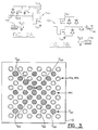
- FIG. 3 is a plan view of a flip-chip containing solder bumps formed according to the method of FIGS. 1A-1l.
- first conductivity type and “second conductivity type” refer to alternative conductivity types such as N or P-type.
- a plurality of active semiconductor devices and circuits are preferably formed at a first face of a semiconductor substrate 10 of first conductivity type, using conventional techniques known to those skilled in the art.
- these devices and circuits may comprise typical CMOS-based input and output circuits 12a, 12b with electrostatic discharge protection (ESD) devices such as input protection diodes and transistors coupled to power supply (Vdd, Vss) potentials.
- ESD electrostatic discharge protection
- These input and output circuits 12a and 12b may be coupled directly to respective input and output signal pads 14a and 14b .
- a plurality of relatively highly doped substrate contact regions 16 of first conductivity type (e.g., N + or P + ) may also be formed at the first face of the semiconductor substrate 10 using conventional techniques. These substrate contact regions 16 are illustrated best by FIGS. 1A-1l.
- One or more "well" regions of second conductivity type (not shown) may also be provided in the substrate 10 .
- a first electrically insulating layer 18 (e.g., SiO 2 ) is preferably formed on the first face of the substrate 10 and then photolithographically patterned.
- the first electrically insulating layer 18 may be patterned to expose the substrate contact regions 16 .
- At least one layer of metallization e.g., aluminum
- a blanket passivation layer 22 is preferably formed on the substrate 10 and patterned to define openings therein which expose the signal and power supply pads, using conventional processing techniques well known to those skilled in the art.
- An ultra-thin plating base layer 24 having a preferred thickness of less than about 0.075 ⁇ m (750 ⁇ ), is then formed on the substrate 10 , as illustrated by FIG. 1C.
- the plating base layer 24 is preferably formed to cover all of the chips and to electrically interconnect all the signal and power supply pads on all the chips together.
- the plating base layer 24 is preferably not formed in contact with a wafer's dicing streets which extend between adjacent chips.
- the plating base layer 24 is preferably formed as a composite metal layer by sputtering a blanket adhesion layer of titanium having a thickness of less than about 375 ⁇ and then sputtering a more highly conductive layer of copper of similar thickness on the adhesion layer.
- a plating template 26 having an array of openings therein is then formed on the plating base layer 24 .
- the array of openings in the plating template 24 define the locations of the array of solder bumps to be formed on the signal and power supply pads.
- a backside wafer contact (not shown) is then attached to a second face of the substrate 10 and then a relatively short duration electroplating step is performed to define an array of wetting layers 28 in the openings in the plating template 24 , as illustrated by FIG. 1E.
- These wetting layers 28 preferably comprise a layer of nickel having a thickness or about 5,000-25,000 ⁇ .
- the electroplating step may be performed by exposing the plating base layer 24 to an electrolytic plating bath, and then biasing the backside wafer contact to draw plating current through the substrate 10 .
- plating current I plate
- plating current l plate
- plating current is preferably drawn vertically through the substrate 10 from the first face to a second face thereof via a first plurality of parallel electrical paths formed by the plating base layer 24 , the plurality of input and output signal pads 14a, 14b and the plurality of input and output circuits 12a, 12b and ESD devices coupled thereto.
- an input device or circuit 12a comprises an insulated gate field effect transistor (e.g., MOSFET) having a gate electrode coupled to an input pad 14a , as illustrated by FIG. 2A
- plating current (l plate ) is preferably drawn as leakage current through the transistor's gate oxide and into the substrate 10 .
- Plating currents may also be drawn as leakage currents through the ESD protection devices. These leakage currents can be substantial when the contributions of all the leakage paths through all the input circuits 12a (and output circuits 12b ) are considered.
- these leakage currents can be drawn through state-of-the-art gate oxides without becoming permanently trapped and inducing threshold voltage (V th ) shifts.
- V th threshold voltage
- plating current is also drawn directly through a plurality of ground pads 14c which are preferably ohmically connected to the substrate 10 through a plurality of highly doped contact regions 16 .
- These ground pads 14c are preferably interspersed closely among the input and output signal pads 14a, 14b to limit the amount of lateral current in the ultra-thin plating base layer 24 .
- the combined contributions of all the plating currents (I plate ) drawn through the substrate contact regions 16 and the active semiconductor devices and circuits 12a, 12b is sufficient to maintain the plating base layer 24 and the underlying pads 14a-14c at uniform potentials even though the plating base layer 24 has a preferred thickness of less than about 0.075 ⁇ m.
- These uniform and typically non-zero potentials cause the rates of electroplating to be highly uniform across the wafer by limiting lateral current flow through the plating base layer 24 .
- an electroplating step is again performed to plate a plurality of PbSn solder bumps 30 on the corresponding plurality of wetting layers 28 .
- the plating current (I plate ) is preferably drawn as leakage current through the input and output circuits 12a, 12b and the ESD protection devices.
- plating current is drawn directly through a plurality of ground pads 14c which are preferably ohmically connected to the substrate 10 through the plurality of highly doped contact regions 16 .
- the substrate 10 is then removed from the plating bath.
- the plating template 26 is then removed using conventional techniques, as illustrated by FIG. 1G. Then, as illustrated best by FIGS.
- the ultra-thin plating base layer 24 is removed using a short duration etching step to expose the passivation layer 22 and electrically isolate the solder bumps 30 from each other.
- the solder bumps 30 can then be reflowed, as illustrated by FIG. 1l, or the reflow step can be performed before the step of etching the plating base layer 24 illustrated by FIG. 1H.
- the present invention is compatible with etch-before-reflow and reflow-before-etch techniques.
- the uniformity of the electroplated solder bumps can also be enhanced by using high density controlled collapse chip connection (C4) ("flip-chip”) technologies and by interspersing the ground and signal pads on each "flip-chip” so that each signal pad has at least one ground pad as a nearest neighbor.
- C4 high density controlled collapse chip connection
- FIG. 3 a preferred arrangement of ground, power and signal pads on a flip-chip is best illustrated by FIG. 3.
- at least 10-25% of the contact pads should be ground pads to maintain I plate at a sufficiently high level during the wetting layer and solder bump electroplating steps.
Landscapes
- Electroplating Methods And Accessories (AREA)
- Internal Circuitry In Semiconductor Integrated Circuit Devices (AREA)
- Electrodes Of Semiconductors (AREA)
- Die Bonding (AREA)
- Wire Bonding (AREA)
Priority Applications (1)
| Application Number | Priority Date | Filing Date | Title |
|---|---|---|---|
| EP20070020495 EP1892754A3 (de) | 1997-05-09 | 1998-04-28 | Verfahren zur Galvanisierung von Löthöckern mit einheitlicher Höhe auf IC-Substraten |
Applications Claiming Priority (2)
| Application Number | Priority Date | Filing Date | Title |
|---|---|---|---|
| US08/854,075 US6117299A (en) | 1997-05-09 | 1997-05-09 | Methods of electroplating solder bumps of uniform height on integrated circuit substrates |
| US854075 | 1997-05-09 |
Related Child Applications (1)
| Application Number | Title | Priority Date | Filing Date |
|---|---|---|---|
| EP20070020495 Division EP1892754A3 (de) | 1997-05-09 | 1998-04-28 | Verfahren zur Galvanisierung von Löthöckern mit einheitlicher Höhe auf IC-Substraten |
Publications (3)
| Publication Number | Publication Date |
|---|---|
| EP0877419A2 true EP0877419A2 (de) | 1998-11-11 |
| EP0877419A3 EP0877419A3 (de) | 1999-08-18 |
| EP0877419B1 EP0877419B1 (de) | 2007-12-05 |
Family
ID=25317657
Family Applications (2)
| Application Number | Title | Priority Date | Filing Date |
|---|---|---|---|
| EP20070020495 Withdrawn EP1892754A3 (de) | 1997-05-09 | 1998-04-28 | Verfahren zur Galvanisierung von Löthöckern mit einheitlicher Höhe auf IC-Substraten |
| EP19980303275 Expired - Lifetime EP0877419B1 (de) | 1997-05-09 | 1998-04-28 | Elektrochemisches Abscheiden von Lötbällen mit einheitlicher Höhe auf Halbleitersubstraten |
Family Applications Before (1)
| Application Number | Title | Priority Date | Filing Date |
|---|---|---|---|
| EP20070020495 Withdrawn EP1892754A3 (de) | 1997-05-09 | 1998-04-28 | Verfahren zur Galvanisierung von Löthöckern mit einheitlicher Höhe auf IC-Substraten |
Country Status (7)
| Country | Link |
|---|---|
| US (1) | US6117299A (de) |
| EP (2) | EP1892754A3 (de) |
| JP (1) | JPH1167804A (de) |
| KR (1) | KR100536927B1 (de) |
| AT (1) | ATE380392T1 (de) |
| DE (1) | DE69838804D1 (de) |
| TW (1) | TW364188B (de) |
Cited By (8)
| Publication number | Priority date | Publication date | Assignee | Title |
|---|---|---|---|---|
| GB2361450A (en) * | 2000-04-19 | 2001-10-24 | Advanced Interconnect Tech Ltd | Forming lead-free solder bump interconnections |
| WO2002095822A3 (en) * | 2001-05-21 | 2003-07-10 | Intel Corp | Method for packaging a microelectronic device using on-die bond pad expansion |
| US6608377B2 (en) * | 2001-01-30 | 2003-08-19 | Samsung Electronics Co., Ltd. | Wafer level package including ground metal layer |
| US6608379B2 (en) * | 2001-11-02 | 2003-08-19 | Institute Of Microelectronics, Et Al. | Enhanced chip scale package for flip chips |
| US6888240B2 (en) | 2001-04-30 | 2005-05-03 | Intel Corporation | High performance, low cost microelectronic circuit package with interposer |
| US6894399B2 (en) | 2001-04-30 | 2005-05-17 | Intel Corporation | Microelectronic device having signal distribution functionality on an interfacial layer thereof |
| US7183658B2 (en) | 2001-09-05 | 2007-02-27 | Intel Corporation | Low cost microelectronic circuit package |
| WO2008020402A3 (en) * | 2006-08-17 | 2008-07-17 | Nxp Bv | Testing for correct undercutting of an electrode during an etching step |
Families Citing this family (51)
| Publication number | Priority date | Publication date | Assignee | Title |
|---|---|---|---|---|
| JP3553791B2 (ja) * | 1998-04-03 | 2004-08-11 | 株式会社ルネサステクノロジ | 接続装置およびその製造方法、検査装置並びに半導体素子の製造方法 |
| US6077405A (en) * | 1998-10-28 | 2000-06-20 | International Business Machines Corporation | Method and apparatus for making electrical contact to a substrate during electroplating |
| TW396462B (en) * | 1998-12-17 | 2000-07-01 | Eriston Technologies Pte Ltd | Bumpless flip chip assembly with solder via |
| DE19907168C1 (de) * | 1999-02-19 | 2000-08-10 | Micronas Intermetall Gmbh | Schichtanordnung sowie Verfahren zu deren Herstellung |
| JP3553413B2 (ja) * | 1999-04-26 | 2004-08-11 | 富士通株式会社 | 半導体装置の製造方法 |
| US6435396B1 (en) * | 2000-04-10 | 2002-08-20 | Micron Technology, Inc. | Print head for ejecting liquid droplets |
| WO2001059842A1 (en) * | 2000-02-10 | 2001-08-16 | International Rectifier Corporation | Vertical conduction flip-chip device with bump contacts on single surface |
| US6878396B2 (en) * | 2000-04-10 | 2005-04-12 | Micron Technology, Inc. | Micro C-4 semiconductor die and method for depositing connection sites thereon |
| KR100367808B1 (ko) * | 2000-08-18 | 2003-01-10 | 씨티에스 컴퓨터 테크놀로지 시스템 코포레이션 | 반도체 장치와 접촉부 형성 방법 |
| US6692629B1 (en) * | 2000-09-07 | 2004-02-17 | Siliconware Precision Industries Co., Ltd. | Flip-chip bumbing method for fabricating solder bumps on semiconductor wafer |
| US6666368B2 (en) | 2000-11-10 | 2003-12-23 | Unitive Electronics, Inc. | Methods and systems for positioning substrates using spring force of phase-changeable bumps therebetween |
| US6348401B1 (en) * | 2000-11-10 | 2002-02-19 | Siliconware Precision Industries Co., Ltd. | Method of fabricating solder bumps with high coplanarity for flip-chip application |
| DE60108413T2 (de) | 2000-11-10 | 2005-06-02 | Unitive Electronics, Inc. | Verfahren zum positionieren von komponenten mit hilfe flüssiger antriebsmittel und strukturen hierfür |
| US6863209B2 (en) | 2000-12-15 | 2005-03-08 | Unitivie International Limited | Low temperature methods of bonding components |
| US6793792B2 (en) * | 2001-01-12 | 2004-09-21 | Unitive International Limited Curaco | Electroplating methods including maintaining a determined electroplating voltage and related systems |
| JP2002222823A (ja) * | 2001-01-29 | 2002-08-09 | Sharp Corp | 半導体集積回路およびその製造方法 |
| US6926818B1 (en) | 2001-09-24 | 2005-08-09 | Taiwan Semiconductor Manufacturing Co., Ltd. | Method to enhance the adhesion between dry film and seed metal |
| KR100825768B1 (ko) * | 2001-10-26 | 2008-04-29 | 삼성전자주식회사 | 범프를 포함하는 반도체 소자 및 그 형성방법 |
| US6960828B2 (en) | 2002-06-25 | 2005-11-01 | Unitive International Limited | Electronic structures including conductive shunt layers |
| US7531898B2 (en) | 2002-06-25 | 2009-05-12 | Unitive International Limited | Non-Circular via holes for bumping pads and related structures |
| US7547623B2 (en) | 2002-06-25 | 2009-06-16 | Unitive International Limited | Methods of forming lead free solder bumps |
| US20040055893A1 (en) * | 2002-09-23 | 2004-03-25 | Applied Materials, Inc. | Wafer backside electrical contact for electrochemical deposition and electrochemical mechanical polishing |
| TW554503B (en) * | 2002-10-23 | 2003-09-21 | Orient Semiconductor Elect Ltd | Fabrication method of solder bump pattern in back-end wafer level package |
| TWI225899B (en) | 2003-02-18 | 2005-01-01 | Unitive Semiconductor Taiwan C | Etching solution and method for manufacturing conductive bump using the etching solution to selectively remove barrier layer |
| JP4047252B2 (ja) * | 2003-06-09 | 2008-02-13 | アルプス電気株式会社 | 薄膜構造体の製造方法 |
| US6951775B2 (en) * | 2003-06-28 | 2005-10-04 | International Business Machines Corporation | Method for forming interconnects on thin wafers |
| WO2005024912A2 (en) * | 2003-09-09 | 2005-03-17 | Intel Corporation | Methods of processing thick ild layers using spray coating or lamination for c4 wafer level thick metal integrated flow |
| US6977435B2 (en) * | 2003-09-09 | 2005-12-20 | Intel Corporation | Thick metal layer integrated process flow to improve power delivery and mechanical buffering |
| US7384531B1 (en) * | 2004-02-19 | 2008-06-10 | Hutchinson Technology Incorporated | Plated ground features for integrated lead suspensions |
| US7226860B2 (en) * | 2004-04-28 | 2007-06-05 | Taiwan Semiconductor Manfacturing Co. Ltd. | Method and apparatus for fabricating metal layer |
| KR100618543B1 (ko) * | 2004-06-15 | 2006-08-31 | 삼성전자주식회사 | 웨이퍼 레벨 적층 패키지용 칩 스케일 패키지 제조 방법 |
| KR100575591B1 (ko) * | 2004-07-27 | 2006-05-03 | 삼성전자주식회사 | 웨이퍼 레벨 적층 패키지용 칩 스케일 패키지 및 그 제조 방법 |
| TWI246135B (en) * | 2005-01-18 | 2005-12-21 | Siliconware Precision Industries Co Ltd | Semiconductor element with under bump metallurgy structure and fabrication method thereof |
| GB0507887D0 (en) * | 2005-04-20 | 2005-05-25 | Rohm & Haas Elect Mat | Immersion method |
| TWI255568B (en) * | 2005-09-15 | 2006-05-21 | Chipmos Technologies Inc | Light emitting diode and fabricating method thereof |
| US7416975B2 (en) * | 2005-09-21 | 2008-08-26 | Novellus Systems, Inc. | Method of forming contact layers on substrates |
| US7674701B2 (en) | 2006-02-08 | 2010-03-09 | Amkor Technology, Inc. | Methods of forming metal layers using multi-layer lift-off patterns |
| US7932615B2 (en) | 2006-02-08 | 2011-04-26 | Amkor Technology, Inc. | Electronic devices including solder bumps on compliant dielectric layers |
| US7768075B2 (en) | 2006-04-06 | 2010-08-03 | Fairchild Semiconductor Corporation | Semiconductor die packages using thin dies and metal substrates |
| US7875804B1 (en) | 2006-09-27 | 2011-01-25 | Hutchinson Technology Incorporated | Plated ground features for integrated lead suspensions |
| US7485564B2 (en) * | 2007-02-12 | 2009-02-03 | International Business Machines Corporation | Undercut-free BLM process for Pb-free and Pb-reduced C4 |
| US7713860B2 (en) * | 2007-10-13 | 2010-05-11 | Wan-Ling Yu | Method of forming metallic bump on I/O pad |
| KR20100038576A (ko) * | 2008-10-06 | 2010-04-15 | 삼성전자주식회사 | 구리 도금용 조성물 및 이를 이용한 구리 배선의 형성 방법 |
| US8183593B2 (en) * | 2009-10-16 | 2012-05-22 | Oracle America, Inc. | Semiconductor die with integrated electro-static discharge device |
| US8354750B2 (en) | 2010-02-01 | 2013-01-15 | Taiwan Semiconductor Manufacturing Company, Ltd. | Stress buffer structures in a mounting structure of a semiconductor device |
| US20150195912A1 (en) | 2014-01-08 | 2015-07-09 | Zhuhai Advanced Chip Carriers & Electronic Substrate Solutions Technologies Co. Ltd. | Substrates With Ultra Fine Pitch Flip Chip Bumps |
| US9728518B2 (en) * | 2014-04-01 | 2017-08-08 | Ati Technologies Ulc | Interconnect etch with polymer layer edge protection |
| US9953908B2 (en) | 2015-10-30 | 2018-04-24 | International Business Machines Corporation | Method for forming solder bumps using sacrificial layer |
| KR101926187B1 (ko) | 2016-12-15 | 2018-12-06 | 스마트모듈러 테크놀러지스 엘엑스 에스에이알엘 | 반도체 패키지의 범프 형성방법 |
| CN111883449B (zh) * | 2020-06-18 | 2022-04-15 | 宁波芯健半导体有限公司 | 一种提高电镀凸块高度均匀性的方法 |
| CN115763282A (zh) * | 2022-11-28 | 2023-03-07 | Tcl华星光电技术有限公司 | 发光基板的制造方法及显示装置 |
Family Cites Families (23)
| Publication number | Priority date | Publication date | Assignee | Title |
|---|---|---|---|---|
| US3625837A (en) * | 1969-09-18 | 1971-12-07 | Singer Co | Electroplating solder-bump connectors on microcircuits |
| US3760238A (en) * | 1972-02-28 | 1973-09-18 | Microsystems Int Ltd | Fabrication of beam leads |
| US4142202A (en) * | 1976-01-31 | 1979-02-27 | Licentia-Patent-Verwaltungs-G.M.B.H. | Multi-layer metal connecting contact and method for making it |
| US4087314A (en) * | 1976-09-13 | 1978-05-02 | Motorola, Inc. | Bonding pedestals for semiconductor devices |
| US4205099A (en) * | 1978-04-14 | 1980-05-27 | Sprague Electric Company | Method for making terminal bumps on semiconductor wafers |
| JPS5773953A (en) * | 1980-10-25 | 1982-05-08 | Nec Home Electronics Ltd | Production of semiconductor device |
| JPS6149432A (ja) * | 1984-08-18 | 1986-03-11 | Matsushita Electric Ind Co Ltd | 半導体装置の製造方法 |
| KR970003915B1 (ko) * | 1987-06-24 | 1997-03-22 | 미다 가쓰시게 | 반도체 기억장치 및 그것을 사용한 반도체 메모리 모듈 |
| US5138438A (en) * | 1987-06-24 | 1992-08-11 | Akita Electronics Co. Ltd. | Lead connections means for stacked tab packaged IC chips |
| JPS6461934A (en) * | 1987-09-02 | 1989-03-08 | Nippon Denso Co | Semiconductor device and manufacture thereof |
| US5162257A (en) * | 1991-09-13 | 1992-11-10 | Mcnc | Solder bump fabrication method |
| JPH05166815A (ja) * | 1991-12-16 | 1993-07-02 | Matsushita Electron Corp | メッキバンプ形成方法及びそれに用いるウエーハメッキ用治具 |
| US5289631A (en) * | 1992-03-04 | 1994-03-01 | Mcnc | Method for testing, burn-in, and/or programming of integrated circuit chips |
| US5342495A (en) * | 1993-02-03 | 1994-08-30 | Vlsi Technology, Inc. | Structure for holding integrated circuit dies to be electroplated |
| KR950004464A (ko) * | 1993-07-15 | 1995-02-18 | 김광호 | 칩 범프의 제조방법 |
| US5508229A (en) * | 1994-05-24 | 1996-04-16 | National Semiconductor Corporation | Method for forming solder bumps in semiconductor devices |
| US5503286A (en) * | 1994-06-28 | 1996-04-02 | International Business Machines Corporation | Electroplated solder terminal |
| US5492863A (en) * | 1994-10-19 | 1996-02-20 | Motorola, Inc. | Method for forming conductive bumps on a semiconductor device |
| US5486282A (en) * | 1994-11-30 | 1996-01-23 | Ibm Corporation | Electroetching process for seed layer removal in electrochemical fabrication of wafers |
| US5597469A (en) * | 1995-02-13 | 1997-01-28 | International Business Machines Corporation | Process for selective application of solder to circuit packages |
| JP2830903B2 (ja) * | 1995-07-21 | 1998-12-02 | 日本電気株式会社 | 半導体デバイスの製造方法 |
| US5736456A (en) * | 1996-03-07 | 1998-04-07 | Micron Technology, Inc. | Method of forming conductive bumps on die for flip chip applications |
| US5662788A (en) * | 1996-06-03 | 1997-09-02 | Micron Technology, Inc. | Method for forming a metallization layer |
-
1997
- 1997-05-09 US US08/854,075 patent/US6117299A/en not_active Expired - Lifetime
-
1998
- 1998-04-28 DE DE69838804T patent/DE69838804D1/de not_active Expired - Lifetime
- 1998-04-28 AT AT98303275T patent/ATE380392T1/de not_active IP Right Cessation
- 1998-04-28 EP EP20070020495 patent/EP1892754A3/de not_active Withdrawn
- 1998-04-28 EP EP19980303275 patent/EP0877419B1/de not_active Expired - Lifetime
- 1998-04-29 TW TW087106640A patent/TW364188B/zh not_active IP Right Cessation
- 1998-05-08 JP JP14238098A patent/JPH1167804A/ja active Pending
- 1998-05-08 KR KR1019980016399A patent/KR100536927B1/ko not_active Expired - Fee Related
Cited By (12)
| Publication number | Priority date | Publication date | Assignee | Title |
|---|---|---|---|---|
| GB2361450A (en) * | 2000-04-19 | 2001-10-24 | Advanced Interconnect Tech Ltd | Forming lead-free solder bump interconnections |
| GB2361450B (en) * | 2000-04-19 | 2002-06-26 | Advanced Interconnect Tech Ltd | Method of forming lead-free bump interconnections |
| SG94808A1 (en) * | 2000-04-19 | 2003-03-18 | Advanced Interconnect Tech Ltd | Method of forming lead-free bump interconnections |
| US6638847B1 (en) | 2000-04-19 | 2003-10-28 | Advanced Interconnect Technology Ltd. | Method of forming lead-free bump interconnections |
| US6608377B2 (en) * | 2001-01-30 | 2003-08-19 | Samsung Electronics Co., Ltd. | Wafer level package including ground metal layer |
| US6888240B2 (en) | 2001-04-30 | 2005-05-03 | Intel Corporation | High performance, low cost microelectronic circuit package with interposer |
| US6894399B2 (en) | 2001-04-30 | 2005-05-17 | Intel Corporation | Microelectronic device having signal distribution functionality on an interfacial layer thereof |
| WO2002095822A3 (en) * | 2001-05-21 | 2003-07-10 | Intel Corp | Method for packaging a microelectronic device using on-die bond pad expansion |
| US7071024B2 (en) | 2001-05-21 | 2006-07-04 | Intel Corporation | Method for packaging a microelectronic device using on-die bond pad expansion |
| US7183658B2 (en) | 2001-09-05 | 2007-02-27 | Intel Corporation | Low cost microelectronic circuit package |
| US6608379B2 (en) * | 2001-11-02 | 2003-08-19 | Institute Of Microelectronics, Et Al. | Enhanced chip scale package for flip chips |
| WO2008020402A3 (en) * | 2006-08-17 | 2008-07-17 | Nxp Bv | Testing for correct undercutting of an electrode during an etching step |
Also Published As
| Publication number | Publication date |
|---|---|
| KR19980086853A (ko) | 1998-12-05 |
| EP0877419A3 (de) | 1999-08-18 |
| US6117299A (en) | 2000-09-12 |
| TW364188B (en) | 1999-07-11 |
| DE69838804D1 (de) | 2008-01-17 |
| EP1892754A3 (de) | 2008-03-19 |
| KR100536927B1 (ko) | 2006-03-24 |
| ATE380392T1 (de) | 2007-12-15 |
| EP0877419B1 (de) | 2007-12-05 |
| JPH1167804A (ja) | 1999-03-09 |
| EP1892754A2 (de) | 2008-02-27 |
Similar Documents
| Publication | Publication Date | Title |
|---|---|---|
| US6117299A (en) | Methods of electroplating solder bumps of uniform height on integrated circuit substrates | |
| US7665652B2 (en) | Electronic devices including metallurgy structures for wire and solder bonding | |
| US10861811B2 (en) | Connector structure and method of forming same | |
| US7297631B2 (en) | Methods of forming electronic structures including conductive shunt layers and related structures | |
| US6848177B2 (en) | Integrated circuit die and an electronic assembly having a three-dimensional interconnection scheme | |
| KR101582355B1 (ko) | 반도체 장치 및 그 제조 방법 | |
| US6977435B2 (en) | Thick metal layer integrated process flow to improve power delivery and mechanical buffering | |
| US6878465B2 (en) | Under bump metallurgy for Lead-Tin bump over copper pad | |
| US7816787B2 (en) | Method of forming low stress multi-layer metallurgical structures and high reliable lead free solder termination electrodes | |
| US6583039B2 (en) | Method of forming a bump on a copper pad | |
| EP2232549B1 (de) | Verfahren zum herstellen einer 3d-halbleiter-ausformstruktur mit einer behälterstruktur | |
| WO2016154315A1 (en) | Metal bond pad with cobalt interconnect layer and solder thereon | |
| US12417992B2 (en) | Chip structure with conductive pillar and method for forming the same | |
| US20030189261A1 (en) | Under-bump-metallurgy layer | |
| US7026234B2 (en) | Parasitic capacitance-preventing dummy solder bump structure and method of making the same | |
| US20030178655A1 (en) | Dual sided power amplifier | |
| GB2095904A (en) | Semiconductor device with built-up low resistance contact and laterally conducting second contact | |
| US11855032B2 (en) | Semiconductor structure and manufacturing method thereof | |
| US7994043B1 (en) | Lead free alloy bump structure and fabrication method | |
| JP2002299366A (ja) | 半導体装置およびその製造方法 | |
| JP3308105B2 (ja) | 半導体集積回路装置およびその製造方法 |
Legal Events
| Date | Code | Title | Description |
|---|---|---|---|
| PUAI | Public reference made under article 153(3) epc to a published international application that has entered the european phase |
Free format text: ORIGINAL CODE: 0009012 |
|
| AK | Designated contracting states |
Kind code of ref document: A2 Designated state(s): AT BE CH DE DK ES FI FR GB IE IT LI NL SE |
|
| AX | Request for extension of the european patent |
Free format text: AL;LT;LV;MK;RO;SI |
|
| PUAL | Search report despatched |
Free format text: ORIGINAL CODE: 0009013 |
|
| AK | Designated contracting states |
Kind code of ref document: A3 Designated state(s): AT BE CH CY DE DK ES FI FR GB GR IE IT LI LU MC NL PT SE |
|
| AX | Request for extension of the european patent |
Free format text: AL;LT;LV;MK;RO;SI |
|
| 17P | Request for examination filed |
Effective date: 20000204 |
|
| AKX | Designation fees paid |
Free format text: AT BE CH DE DK ES FI FR GB IE IT LI NL |
|
| RBV | Designated contracting states (corrected) |
Designated state(s): AT BE CH DE DK ES FI FR GB IE IT LI NL SE |
|
| RAP1 | Party data changed (applicant data changed or rights of an application transferred) |
Owner name: UNITIVE INTERNATIONAL LIMITED |
|
| 17Q | First examination report despatched |
Effective date: 20041013 |
|
| 17Q | First examination report despatched |
Effective date: 20041013 |
|
| GRAP | Despatch of communication of intention to grant a patent |
Free format text: ORIGINAL CODE: EPIDOSNIGR1 |
|
| GRAS | Grant fee paid |
Free format text: ORIGINAL CODE: EPIDOSNIGR3 |
|
| GRAA | (expected) grant |
Free format text: ORIGINAL CODE: 0009210 |
|
| AK | Designated contracting states |
Kind code of ref document: B1 Designated state(s): AT BE CH DE DK ES FI FR GB IE IT LI NL SE |
|
| REG | Reference to a national code |
Ref country code: GB Ref legal event code: FG4D |
|
| REG | Reference to a national code |
Ref country code: IE Ref legal event code: FG4D |
|
| REG | Reference to a national code |
Ref country code: CH Ref legal event code: EP |
|
| REF | Corresponds to: |
Ref document number: 69838804 Country of ref document: DE Date of ref document: 20080117 Kind code of ref document: P |
|
| PG25 | Lapsed in a contracting state [announced via postgrant information from national office to epo] |
Ref country code: SE Free format text: LAPSE BECAUSE OF FAILURE TO SUBMIT A TRANSLATION OF THE DESCRIPTION OR TO PAY THE FEE WITHIN THE PRESCRIBED TIME-LIMIT Effective date: 20080305 Ref country code: NL Free format text: LAPSE BECAUSE OF FAILURE TO SUBMIT A TRANSLATION OF THE DESCRIPTION OR TO PAY THE FEE WITHIN THE PRESCRIBED TIME-LIMIT Effective date: 20071205 Ref country code: LI Free format text: LAPSE BECAUSE OF FAILURE TO SUBMIT A TRANSLATION OF THE DESCRIPTION OR TO PAY THE FEE WITHIN THE PRESCRIBED TIME-LIMIT Effective date: 20071205 Ref country code: ES Free format text: LAPSE BECAUSE OF FAILURE TO SUBMIT A TRANSLATION OF THE DESCRIPTION OR TO PAY THE FEE WITHIN THE PRESCRIBED TIME-LIMIT Effective date: 20080316 Ref country code: CH Free format text: LAPSE BECAUSE OF FAILURE TO SUBMIT A TRANSLATION OF THE DESCRIPTION OR TO PAY THE FEE WITHIN THE PRESCRIBED TIME-LIMIT Effective date: 20071205 |
|
| PG25 | Lapsed in a contracting state [announced via postgrant information from national office to epo] |
Ref country code: FI Free format text: LAPSE BECAUSE OF FAILURE TO SUBMIT A TRANSLATION OF THE DESCRIPTION OR TO PAY THE FEE WITHIN THE PRESCRIBED TIME-LIMIT Effective date: 20071205 |
|
| NLV1 | Nl: lapsed or annulled due to failure to fulfill the requirements of art. 29p and 29m of the patents act | ||
| REG | Reference to a national code |
Ref country code: CH Ref legal event code: PL |
|
| PG25 | Lapsed in a contracting state [announced via postgrant information from national office to epo] |
Ref country code: AT Free format text: LAPSE BECAUSE OF FAILURE TO SUBMIT A TRANSLATION OF THE DESCRIPTION OR TO PAY THE FEE WITHIN THE PRESCRIBED TIME-LIMIT Effective date: 20071205 |
|
| PG25 | Lapsed in a contracting state [announced via postgrant information from national office to epo] |
Ref country code: BE Free format text: LAPSE BECAUSE OF FAILURE TO SUBMIT A TRANSLATION OF THE DESCRIPTION OR TO PAY THE FEE WITHIN THE PRESCRIBED TIME-LIMIT Effective date: 20071205 |
|
| EN | Fr: translation not filed | ||
| PLBE | No opposition filed within time limit |
Free format text: ORIGINAL CODE: 0009261 |
|
| STAA | Information on the status of an ep patent application or granted ep patent |
Free format text: STATUS: NO OPPOSITION FILED WITHIN TIME LIMIT |
|
| PG25 | Lapsed in a contracting state [announced via postgrant information from national office to epo] |
Ref country code: DK Free format text: LAPSE BECAUSE OF FAILURE TO SUBMIT A TRANSLATION OF THE DESCRIPTION OR TO PAY THE FEE WITHIN THE PRESCRIBED TIME-LIMIT Effective date: 20071205 Ref country code: DE Free format text: LAPSE BECAUSE OF FAILURE TO SUBMIT A TRANSLATION OF THE DESCRIPTION OR TO PAY THE FEE WITHIN THE PRESCRIBED TIME-LIMIT Effective date: 20080306 |
|
| 26N | No opposition filed |
Effective date: 20080908 |
|
| GBPC | Gb: european patent ceased through non-payment of renewal fee |
Effective date: 20080428 |
|
| PG25 | Lapsed in a contracting state [announced via postgrant information from national office to epo] |
Ref country code: IE Free format text: LAPSE BECAUSE OF NON-PAYMENT OF DUE FEES Effective date: 20080428 Ref country code: FR Free format text: LAPSE BECAUSE OF FAILURE TO SUBMIT A TRANSLATION OF THE DESCRIPTION OR TO PAY THE FEE WITHIN THE PRESCRIBED TIME-LIMIT Effective date: 20081003 |
|
| PG25 | Lapsed in a contracting state [announced via postgrant information from national office to epo] |
Ref country code: GB Free format text: LAPSE BECAUSE OF NON-PAYMENT OF DUE FEES Effective date: 20080428 |
|
| PG25 | Lapsed in a contracting state [announced via postgrant information from national office to epo] |
Ref country code: IT Free format text: LAPSE BECAUSE OF NON-PAYMENT OF DUE FEES Effective date: 20080430 |