EP0877438A1 - Elément de circuit haute fréquence - Google Patents
Elément de circuit haute fréquence Download PDFInfo
- Publication number
- EP0877438A1 EP0877438A1 EP98108245A EP98108245A EP0877438A1 EP 0877438 A1 EP0877438 A1 EP 0877438A1 EP 98108245 A EP98108245 A EP 98108245A EP 98108245 A EP98108245 A EP 98108245A EP 0877438 A1 EP0877438 A1 EP 0877438A1
- Authority
- EP
- European Patent Office
- Prior art keywords
- resonator
- circuit element
- frequency circuit
- input
- coupling
- Prior art date
- Legal status (The legal status is an assumption and is not a legal conclusion. Google has not performed a legal analysis and makes no representation as to the accuracy of the status listed.)
- Granted
Links
Images




Classifications
-
- H—ELECTRICITY
- H01—ELECTRIC ELEMENTS
- H01P—WAVEGUIDES; RESONATORS, LINES, OR OTHER DEVICES OF THE WAVEGUIDE TYPE
- H01P7/00—Resonators of the waveguide type
- H01P7/08—Strip line resonators
-
- H—ELECTRICITY
- H01—ELECTRIC ELEMENTS
- H01P—WAVEGUIDES; RESONATORS, LINES, OR OTHER DEVICES OF THE WAVEGUIDE TYPE
- H01P7/00—Resonators of the waveguide type
- H01P7/08—Strip line resonators
- H01P7/082—Microstripline resonators
-
- H—ELECTRICITY
- H01—ELECTRIC ELEMENTS
- H01P—WAVEGUIDES; RESONATORS, LINES, OR OTHER DEVICES OF THE WAVEGUIDE TYPE
- H01P1/00—Auxiliary devices
- H01P1/20—Frequency-selective devices, e.g. filters
- H01P1/201—Filters for transverse electromagnetic waves
- H01P1/203—Strip line filters
-
- H—ELECTRICITY
- H01—ELECTRIC ELEMENTS
- H01P—WAVEGUIDES; RESONATORS, LINES, OR OTHER DEVICES OF THE WAVEGUIDE TYPE
- H01P7/00—Resonators of the waveguide type
- H01P7/10—Dielectric resonators
-
- Y—GENERAL TAGGING OF NEW TECHNOLOGICAL DEVELOPMENTS; GENERAL TAGGING OF CROSS-SECTIONAL TECHNOLOGIES SPANNING OVER SEVERAL SECTIONS OF THE IPC; TECHNICAL SUBJECTS COVERED BY FORMER USPC CROSS-REFERENCE ART COLLECTIONS [XRACs] AND DIGESTS
- Y10—TECHNICAL SUBJECTS COVERED BY FORMER USPC
- Y10S—TECHNICAL SUBJECTS COVERED BY FORMER USPC CROSS-REFERENCE ART COLLECTIONS [XRACs] AND DIGESTS
- Y10S505/00—Superconductor technology: apparatus, material, process
- Y10S505/70—High TC, above 30 k, superconducting device, article, or structured stock
-
- Y—GENERAL TAGGING OF NEW TECHNOLOGICAL DEVELOPMENTS; GENERAL TAGGING OF CROSS-SECTIONAL TECHNOLOGIES SPANNING OVER SEVERAL SECTIONS OF THE IPC; TECHNICAL SUBJECTS COVERED BY FORMER USPC CROSS-REFERENCE ART COLLECTIONS [XRACs] AND DIGESTS
- Y10—TECHNICAL SUBJECTS COVERED BY FORMER USPC
- Y10S—TECHNICAL SUBJECTS COVERED BY FORMER USPC CROSS-REFERENCE ART COLLECTIONS [XRACs] AND DIGESTS
- Y10S505/00—Superconductor technology: apparatus, material, process
- Y10S505/70—High TC, above 30 k, superconducting device, article, or structured stock
- Y10S505/701—Coated or thin film device, i.e. active or passive
-
- Y—GENERAL TAGGING OF NEW TECHNOLOGICAL DEVELOPMENTS; GENERAL TAGGING OF CROSS-SECTIONAL TECHNOLOGIES SPANNING OVER SEVERAL SECTIONS OF THE IPC; TECHNICAL SUBJECTS COVERED BY FORMER USPC CROSS-REFERENCE ART COLLECTIONS [XRACs] AND DIGESTS
- Y10—TECHNICAL SUBJECTS COVERED BY FORMER USPC
- Y10S—TECHNICAL SUBJECTS COVERED BY FORMER USPC CROSS-REFERENCE ART COLLECTIONS [XRACs] AND DIGESTS
- Y10S505/00—Superconductor technology: apparatus, material, process
- Y10S505/825—Apparatus per se, device per se, or process of making or operating same
- Y10S505/866—Wave transmission line, network, waveguide, or microwave storage device
Definitions
- the present invention relates to a high-frequency circuit element, such as a resonator, a filter or the like, used for a high-frequency signal processor in communication systems, etc.
- a high-frequency circuit element such as a resonator, a filter or the like, is an essential component in high-frequency communication systems.
- the main examples of high-frequency circuit elements such as resonators, filters or the like presently used are those using a dielectric resonator, those using a transmission line structure (a microstrip structure or a strip line structure), and those using a surface acoustic wave element.
- those using a transmission line structure are small and can be applied to frequencies as high as microwaves or milliwaves.
- they have a two-dimensional structure formed on a substrate and easily can be combined with other circuits or elements, and therefore they are widely used.
- a half-wavelength resonator with a transmission line is most widely used as this type of resonator. Also, by coupling a plurality of these half-wavelength resonators, a high-frequency circuit element such as a filter or the like is formed (Minute Explanation Examples/Exercises Microwaves Circuit Tokyo Electrical Engineering College Publishing Office).
- a transmission line structure includes those using a planar circuit structure.
- the representative examples are those constructing various high-frequency circuits by using a disc type resonator (Papers of Institute of Electronics and Communication Engineers of Japan, 72/8 Vol.55-B No.8 "Analysis of Microwave Planar Circuit” Tanroku MIYOSHI, Takaaki OOKOSHI).
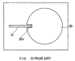
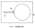
- the line width of the point 31a of an input-output line 31 is broadened, and the point 31a having the broadened line width is located facing the peripheral part of the resonator 30. This enables the degree of input-output coupling to be increased by increasing the coupling capacitance.
- the present invention aims to solve the problems mentioned above in the prior art.
- the object of the present invention is to provide a high-frequency circuit element that can realize a high degree of input-output coupling without causing an increase in loss and irregularity in impedance.
- an aspect of a high-frequency circuit element comprises at least one resonator having a planar circuit structure and at least one input-output line, and is characterized in that the input-output line has a side edge and a part of the side edge of the input-output line is located along a coupling part on the peripheral part of the resonator and spaced from the resonator by a gap part.
- distributed coupling can be made by locating a part of the side edge of the input-output line along the coupling part on the peripheral part of the resonator, and spaced therefrom through the gap part.
- the input-output line has a substantially uniform width.
- a resonator having any shape such as a round resonator, an elliptical resonator, a polygonal resonator or the like, can be used as the resonator in a planar circuit structure.
- the length of the coupling part defines the angle with respect to the center of the resonator. It is preferable that the angle is set in the range of 5-30 o .
- the distance between the coupling part on the periphery of the resonator and the input-output line (the gap part) is set in the range of 10-500 ⁇ m.
- the high-frequency circuit element of the present invention has a microstrip structure or a strip line structure.
- the microstrip structure is simple in structure and has good coherency with other circuits.
- the strip line structure enables a high-frequency circuit element having small loss to be realized, since the radiation loss is very small.
- an elliptical resonator is used as a resonator in a planar circuit structure and two input-output lines are coupled to the resonator, wherein the coupling parts are in the vicinity of the intersections of the periphery of the resonator with the major axis of the ellipse and the minor axis of the ellipse respectively and are provided at the positions about 90 o apart from each other with respect to the center of the resonator.
- This preferable example can be operated as a band pass filter. It is conceivable that it can be operated as a two-stage resonator coupled filter by utilizing the coupling between two resonance modes of the elliptical resonator.
- a superconductor is used as a material of the resonator. According to this preferable example, a high-frequency circuit element having small loss and excellent power endurance characteristics can be realized.
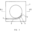
- FIG. 1 is a plan view showing a first embodiment of a high-frequency circuit element according to the present invention.
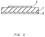
- FIG. 2 is a cross-sectional view along line II-II in FIG. 1.
- FIG. 3 is a graph showing reflection characteristics of a high-frequency circuit element of the first embodiment of the present invention.
- FIG. 4 is a plan view showing another aspect of the first embodiment of a high-frequency circuit element according to the present invention.
- FIG. 5 is a graph showing reflection characteristics of another aspect of a high-frequency circuit element of the first embodiment of the present invention.
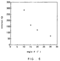
- FIG. 6 is a graph showing the relationship between the length of the coupling part and the degree of input-output coupling in another aspect of a high-frequency circuit element of the first embodiment of the present invention.
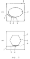
- FIG. 7 (a) and (b) are plan views showing additional aspects of a high-frequency circuit element of the first embodiment of the present invention.
- FIG. 8 is a plan view showing a second embodiment of a high-frequency circuit element according to the present invention.
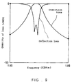
- FIG. 9 is a graph showing input-output characteristics of a high-frequency circuit element of the second embodiment of the present invention.
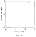
- FIG. 10 is a graph showing insertion loss characteristics with respect to input power in a high-frequency circuit element of the second embodiment of the present invention.
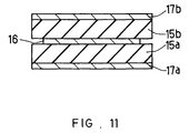
- FIG. 11 is a cross-sectional view showing a high-frequency circuit element having a strip line structure of the present invention.
- FIG. 12 is a plan view showing an example of a high-frequency circuit element in the prior art.
- FIG. 13 is a plan view showing another example of a high-frequency circuit element in the prior art.
- FIG. 14 is a graph showing a comparative example of the relationship between the length of the coupling part and the degree of input-output coupling in a high-frequency circuit element.
- FIG. 1 is a plan view showing a first embodiment of a high-frequency circuit element according to the present invention.
- FIG. 2 is a cross-sectional view along line II-II in FIG. 1.
- a round resonator 2 made of a conductor film is formed at the center on a substrate 1 made of a dielectric monocrystal or the like by using, for example, a vacuum evaporation method and etching.
- An input-output line 3 made of a conductor film is formed on the same surface of the substrate 1 as the surface on which the resonator 2 is formed by using, for example, a vacuum evaporation method and etching.
- the input-output line 3 has a side edge and its line width is uniform.
- a part of the side edge of the input-output line 3 is located along a coupling part 4 on the peripheral part of the resonator 2 and spaced from the resonator by a gap part 5.
- a ground plane 6 made of a conductor film is formed on the entire back surface of the substrate 1 by using, for example, a vacuum evaporation method. This enables a high-frequency circuit element having a microstrip structure to be realized.
- a high-temperature oxide superconductor represented by a yttrium (Y) family superconductor such as YBa 2 Cu 3 O x or the like, a bismuth (Bi) family superconductor such as Bi 2 Sr 2 Ca 2 Cu 3 O x or the like, a thallium (Tl) family superconductor such as Tl 2 Ba 2 CaCu 2 O x or the like; a metallic superconductor such as Nb or the like; or a metal such as gold, copper or the like, etc.
- Y yttrium
- Bi bismuth
- Tl thallium
- metallic superconductor such as Nb or the like
- a metal such as gold, copper or the like, etc.
- the high-frequency signal When inputting a high-frequency signal from a terminal part 7 of the input-output line 3 in a high-frequency circuit element having the structure mentioned above, the high-frequency signal couples with the resonator 2 at the coupling part 4, thus inducing resonance operation.
- the characteristic inherent in a resonance circuit that great absorption occurs at the resonance frequency of the resonator 2 can be obtained as shown in FIG. 3.
- a conventional high-frequency circuit element shown in FIGS. 12 and 13 utilizes the effect of capacitive coupling alone depending on the capacity at a coupling part.
- the effect of distributed coupling by a magnetic field is added.
- the distributed coupling can be made by locating a part of the side edge of the input-output line 3 along the coupling part 4 on the peripheral part of the resonator 2, and spaced therefrom through the gap part 5.
- FIG. 4 is a plan view showing another aspect of the first embodiment of the high-frequency circuit element according to the present invention.
- a round resonator 2 made of a thallium-based high-temperature oxide superconductor having a thickness of 0.7 ⁇ m is formed at the center on a substrate 1 made of a lanthanum alumina (LaAlO 3 ) monocrystal having a thickness of 0.5 mm.
- the radius of the resonator 2 is 9.53 mm.
- An input-output line 3 also made of a thallium-based high-temperature oxide superconductor having a thickness of 0.7 ⁇ m and a line width of 0.175 mm is formed on the same surface of the substrate 1 as the surface on which the resonator 2 is formed.
- a part of the side edge of the input-output line 3 is located along the coupling part 4 on the peripheral part of the resonator 2, spaced from the resonator by the gap part 5.
- the distance between the coupling part on the periphery of the resonator and the input-output line (the gap part 5) is 20 ⁇ m.
- the length of the coupling part 4 is indicated by the angle ⁇ seen with respect to the center of the resonator 2.
- a ground plane (not shown in the figure) also made of a thallium-based high-temperature oxide superconductor having a thickness of 0.7 ⁇ m is formed on the entire back surface of the substrate 1.
- FIG. 6 the change in the degree of input-output coupling when changing the angle ⁇ is shown.
- the higher degree of input-output coupling can be obtained as the external Q of the resonance circuit becomes small. Therefore, the degree of input-output coupling herein is indicated by the external Q of the resonance circuit.
- the degree of input-output coupling is indicated by the external Q of the resonance circuit.
- the degree of input-output coupling increases.
- the change in the degree of input-output coupling in the conventional high-frequency element shown in FIG. 13 is shown in FIG. 14.
- the opening angle of the point of an input-output line 31 is indicated by an angle ⁇ seen with respect to the center of a disc resonator 30.
- the distance between the point of the input-output line 31 and the disc resonator 30 (the gap part) is set to 20 ⁇ m as in FIG. 4.
- the structure is the same as that in FIG. 4 except for the input-output coupling part.
- the angle ⁇ when making the angle ⁇ wider in the conventional high-frequency circuit element shown in FIG. 13, the highest degree of input-output coupling (the external Q of about 450) can be obtained in the vicinity of 20° .
- the angle ⁇ is made wider than that, on the contrary, the external Q becomes greater.
- the degree of input-output coupling becomes lower when making the angle ⁇ wider than 20° .
- the intrinsic impedance of the input-output line 31 changes rapidly when the line width of the point of the input-output line 31 becomes broad and therefore an input-output signal is reflected, the degree of input-output coupling becomes low when making the angle ⁇ wide to some extent. Therefore, when making a comparison under the same conditions, it is possible to decrease the external Q to around 100 in the structure of a high-frequency circuit element according to the present embodiment, but it is impossible to obtain a high degree of input-output coupling having the external Q of 450 or less in the structure of the conventional high-frequency element shown in FIG. 13.
- the structure of the present embodiment is very effective, since a relatively high degree of input-output coupling is generally required in resonator coupling type high-frequency filters.
- the present embodiment was described referring to an example using the round resonator 2 as a resonator in a planar circuit structure.
- the present invention is not always limited to this configuration.
- a resonator in a planar circuit structure a resonator having any shape such as, for example, an elliptical resonator shown in FIG. 7(a) and a polygonal resonator shown in FIG. 7(b) can be used besides the round resonator.
- a high-frequency circuit element using a resonator having such a shape is also effective due to the same reasons as mentioned above.
- the present embodiment was described referring to an example using a high-frequency circuit element comprising one resonator 2 and one input-output line 3.
- the present invention is not always limited to this configuration.
- the present invention can be applied to, for example, a high-frequency circuit element such as a multistage filter using a plurality of resonators and a plurality of input-output lines and a high-frequency circuit element including a resonator and an input-output line as its part, and the same effectiveness can be exhibited.
- FIG. 8 is a plan view showing a second embodiment of a high-frequency circuit element according to the present invention.
- an elliptical resonator 9 made of a conductor film is formed at the center on a substrate 8 made of a dielectric monocrystal or the like by using, for example, a vacuum evaporation method and etching.
- the lengths of the major axis 12 and the minor axis 13 of the elliptical resonator 9 are set to 19.07 mm and 18.93 mm respectively.
- input-output lines 10a and 10b made of conductor films are formed on the same surface of the substrate 8 as the surface on which the resonator 9 is formed.
- the input-output lines 10a and 10b have side edges and their line widths are uniform.
- a part of the side edges of the input-output lines 10a and 10b is located along the coupling parts 11a and 11b on the peripheral part of the resonator 9, spaced from the resonator by the gap parts 14a and 14b respectively.
- coupling parts 11a and 11b are in the vicinity of the intersections of the periphery of the resonator 9 with the major axis 12 and the minor axis 13 respectively and are located at the positions that located 90° apart from each other as seen with respect to the center of the resonator 9. Both lengths of the coupling parts 11a and 11b are set to the lengths corresponding to an angle of 18° seen from the center of the resonator 9.
- a ground plane (not shown in the figure) made of a conductor film is formed by using, for example, a vacuum evaporation method. This realizes a high-frequency circuit element having a microstrip structure.
- FIG. 9 shows input-output characteristics for a high-frequency circuit element having such a structure as mentioned above.
- a flat transmission characteristic can be obtained in the vicinity of 1.9 GHz in this element. Therefore, it can be found that the element operates as a band pass filter.
- the element can be operated as a two-stage resonator coupled filter by utilizing the coupling between two resonant modes of an elliptical resonator.
- the peripheral part of the elliptical resonator is very smooth and the effect of current concentration within the resonator is small. Therefore, in the case of using an ordinary metal as a material of the resonator, the loss is smaller than that in the conventional structure.
- FIG. 10 shows the dependence on input power of insertion loss in a passing band of a high-frequency circuit element having such a structure as mentioned above.
- a HP85108A pulsed RF network analyzer system manufactured by Hewlett Packard was used for the measurement. In this case, the measurement was conducted using a pulsed power signal having a pulse width of 2 ⁇ sec. so as not to be affected by generating heat in a cable for inputting-outputting signals into the element part.
- the environmental tempertature was 20 kelvin.
- no clear change in the insertion loss for the input power up to +50 dBm (100W) was found.
- each of numerals 15a and 15b indicates a substrate
- numeral 16 indicates a resonator
- each of numerals 17a and 17b indicates a ground plane.
- the strip line structure is a complex structure compared to the microstrip structure. However, the radiation loss becomes small and therefore the characteristics of the element can be improved.
- a metal-based material for example, a Pb-based material such as Pb, PbIn or the like, and a Nb-based material such as Nb, NbN, Nb 3 Ge or the like
- a high-temperature oxide superconductor for example, Ba 2 YCu 3 O 7 whose temperature condition is relatively lenient.
- a resonator having a planar circuit structure is used that can effectively relieve the concentration of high-frequency current at the peripheral part of the resonator where the current is most extremely concentrated in the conventional structure.
- a high degree of input-output coupling can be obtained without changing the peripheral shape. Therefore, the maximum electric current density in the case of handling a high-frequency signal having the same power becomes lower than that in the conventional one. Consequently, in the case of constructing a high-frequency circuit element of the present invention using a superconductor having the same critical current density, it becomes possible to handle a high-frequency signal having further higher power. Thus, the effectiveness of the present invention is extremely high.
Landscapes
- Physics & Mathematics (AREA)
- Electromagnetism (AREA)
- Control Of Motors That Do Not Use Commutators (AREA)
Applications Claiming Priority (3)
| Application Number | Priority Date | Filing Date | Title |
|---|---|---|---|
| JP11785997 | 1997-05-08 | ||
| JP117859/97 | 1997-05-08 | ||
| JP11785997A JP3518249B2 (ja) | 1997-05-08 | 1997-05-08 | 高周波回路素子 |
Publications (2)
| Publication Number | Publication Date |
|---|---|
| EP0877438A1 true EP0877438A1 (fr) | 1998-11-11 |
| EP0877438B1 EP0877438B1 (fr) | 2004-12-22 |
Family
ID=14722072
Family Applications (1)
| Application Number | Title | Priority Date | Filing Date |
|---|---|---|---|
| EP98108245A Expired - Lifetime EP0877438B1 (fr) | 1997-05-08 | 1998-05-06 | Elément de circuit haute fréquence |
Country Status (6)
| Country | Link |
|---|---|
| US (1) | US6381478B2 (fr) |
| EP (1) | EP0877438B1 (fr) |
| JP (1) | JP3518249B2 (fr) |
| KR (1) | KR100381853B1 (fr) |
| CN (1) | CN1188927C (fr) |
| DE (1) | DE69828217T2 (fr) |
Families Citing this family (7)
| Publication number | Priority date | Publication date | Assignee | Title |
|---|---|---|---|---|
| US7008397B2 (en) * | 2002-02-13 | 2006-03-07 | Percardia, Inc. | Cardiac implant and methods |
| CN1310375C (zh) * | 2003-03-28 | 2007-04-11 | 松下电器产业株式会社 | 高频电路元件 |
| JP4171015B2 (ja) * | 2005-09-29 | 2008-10-22 | 株式会社東芝 | フィルタ及びこれを用いた無線通信装置 |
| JP4822970B2 (ja) * | 2006-07-27 | 2011-11-24 | 富士通株式会社 | 分割型マイクロストリップライン共振器およびこれを用いたフィルタ |
| JP4769753B2 (ja) | 2007-03-27 | 2011-09-07 | 富士通株式会社 | 超伝導フィルタデバイス |
| JP5369905B2 (ja) * | 2009-06-02 | 2013-12-18 | 富士通株式会社 | 帯域除去フィルタ |
| CN102739161B (zh) * | 2011-04-11 | 2015-03-04 | 南通大学 | 一种宽带频率可调环形谐振器 |
Citations (6)
| Publication number | Priority date | Publication date | Assignee | Title |
|---|---|---|---|---|
| JPS61189703A (ja) | 1985-02-18 | 1986-08-23 | Matsushita Electric Ind Co Ltd | 誘電体共振器装置 |
| JPS63159901U (fr) | 1987-04-09 | 1988-10-19 | ||
| SU1679570A1 (ru) * | 1988-10-25 | 1991-09-23 | Харьковский государственный университет им.А.М.Горького | Управл емый СВЧ фильтр |
| SU1683099A2 (ru) * | 1989-04-26 | 1991-10-07 | Московский институт электронной техники | Микрополосковый фильтр |
| EP0660438A2 (fr) * | 1993-12-27 | 1995-06-28 | Matsushita Electric Industrial Co., Ltd. | Résonateur et élément de circuit hyperfréquence l'utilisant |
| JPH08186415A (ja) | 1994-12-20 | 1996-07-16 | Korea Electron Telecommun | マイクロウェーブシステム用共振器 |
Family Cites Families (6)
| Publication number | Priority date | Publication date | Assignee | Title |
|---|---|---|---|---|
| JPS60253302A (ja) * | 1984-05-30 | 1985-12-14 | Nec Corp | リング型フイルタ |
| JPS61128602A (ja) * | 1984-11-28 | 1986-06-16 | Pioneer Answerphone Mfg Corp | マイクロ波用フイルタ |
| JPS62298202A (ja) * | 1986-06-18 | 1987-12-25 | Matsushita Electric Ind Co Ltd | リング形共振器 |
| DE3931441A1 (de) * | 1989-09-21 | 1991-04-04 | Forschungszentrum Juelich Gmbh | Sensor zum messen von magnetischem fluss |
| US5172084A (en) | 1991-12-18 | 1992-12-15 | Space Systems/Loral, Inc. | Miniature planar filters based on dual mode resonators of circular symmetry |
| US5750473A (en) * | 1995-05-11 | 1998-05-12 | E. I. Du Pont De Nemours And Company | Planar high temperature superconductor filters with backside coupling |
-
1997
- 1997-05-08 JP JP11785997A patent/JP3518249B2/ja not_active Expired - Fee Related
-
1998
- 1998-05-05 US US09/073,102 patent/US6381478B2/en not_active Expired - Lifetime
- 1998-05-06 DE DE69828217T patent/DE69828217T2/de not_active Expired - Lifetime
- 1998-05-06 EP EP98108245A patent/EP0877438B1/fr not_active Expired - Lifetime
- 1998-05-07 KR KR10-1998-0016339A patent/KR100381853B1/ko not_active Expired - Fee Related
- 1998-05-07 CN CNB981079504A patent/CN1188927C/zh not_active Expired - Fee Related
Patent Citations (6)
| Publication number | Priority date | Publication date | Assignee | Title |
|---|---|---|---|---|
| JPS61189703A (ja) | 1985-02-18 | 1986-08-23 | Matsushita Electric Ind Co Ltd | 誘電体共振器装置 |
| JPS63159901U (fr) | 1987-04-09 | 1988-10-19 | ||
| SU1679570A1 (ru) * | 1988-10-25 | 1991-09-23 | Харьковский государственный университет им.А.М.Горького | Управл емый СВЧ фильтр |
| SU1683099A2 (ru) * | 1989-04-26 | 1991-10-07 | Московский институт электронной техники | Микрополосковый фильтр |
| EP0660438A2 (fr) * | 1993-12-27 | 1995-06-28 | Matsushita Electric Industrial Co., Ltd. | Résonateur et élément de circuit hyperfréquence l'utilisant |
| JPH08186415A (ja) | 1994-12-20 | 1996-07-16 | Korea Electron Telecommun | マイクロウェーブシステム用共振器 |
Non-Patent Citations (5)
| Title |
|---|
| F.C. DE RONDE ET AL.: "MIC BANDFILTERS USING OPEN-RING RESONATORS", 4TH EUROPEAN MICROWAVE CONFERENCE- PROCEEDINGS, 10 September 1974 (1974-09-10) - 13 September 1974 (1974-09-13), Montreux (CH), pages 531 - 535, XP002074769 * |
| JANSEN R: "HIGH-ORDER FINITE ELEMENT POLYNOMIALS IN THE COMPUTER ANALYSIS OF ARBITRARILY SHAPED MICROSTRIP RESONATORS", ARCHIV FUR ELEKTRONIK UND UBERTRAGUNGSTECHNIK, vol. 39, no. 2, February 1976 (1976-02-01), pages 71 - 79, XP002039570 * |
| SOVIET PATENTS ABSTRACTS Section EI Week 9228, 26 August 1992 Derwent World Patents Index; Class W02, AN 9223280028, XP002074771 * |
| SOVIET PATENTS ABSTRACTS Section EI Week 9233, 30 September 1992 Derwent World Patents Index; Class W02, AN 9227566033, XP002074770 * |
| WALLACE W J ET AL: "MICROSTRIP RESONATORS FOR ELECTRON-SPIN RESONANCE", REVIEW OF SCIENTIFIC INSTRUMENTS, vol. 62, no. 7, 1 July 1991 (1991-07-01), pages 1754 - 1766, XP000240350 * |
Also Published As
| Publication number | Publication date |
|---|---|
| CN1202021A (zh) | 1998-12-16 |
| US6381478B2 (en) | 2002-04-30 |
| JPH10308611A (ja) | 1998-11-17 |
| KR100381853B1 (ko) | 2003-07-10 |
| CN1188927C (zh) | 2005-02-09 |
| DE69828217D1 (de) | 2005-01-27 |
| EP0877438B1 (fr) | 2004-12-22 |
| JP3518249B2 (ja) | 2004-04-12 |
| KR19980086834A (ko) | 1998-12-05 |
| DE69828217T2 (de) | 2005-12-15 |
| US20020004462A1 (en) | 2002-01-10 |
Similar Documents
| Publication | Publication Date | Title |
|---|---|---|
| EP1026772B1 (fr) | Elément de circuit haute fréquence | |
| US6122533A (en) | Superconductive planar radio frequency filter having resonators with folded legs | |
| WO1998000880A9 (fr) | Filtre planaire de radiofrequences | |
| US6823201B2 (en) | Superconducting microstrip filter having current density reduction parts | |
| US5164358A (en) | Superconducting filter with reduced electromagnetic leakage | |
| EP0567407B1 (fr) | Dispositif micro-ondes en matériau supraconducteur d'oxyde | |
| EP0877438B1 (fr) | Elément de circuit haute fréquence | |
| JPH1013105A (ja) | 高周波フィルタ | |
| US6252475B1 (en) | High-frequency circuit element | |
| JP2898462B2 (ja) | 高周波フィルタ | |
| US7457651B2 (en) | Dual mode filter based on smoothed contour resonators | |
| JP4167187B2 (ja) | フィルタ | |
| JP4125842B2 (ja) | 高周波フィルタ | |
| JPH05160616A (ja) | 薄膜共振器 | |
| KR100313893B1 (ko) | 협대역 초전도 대역 통과 필터 | |
| KR100335098B1 (ko) | 마이크로스트립 초전도 필터 | |
| JPH07336106A (ja) | 端結合フィルタ実装構造体 | |
| US20020005766A1 (en) | RF resonator | |
| US20030151466A1 (en) | Elliptical resonators and radio frequency filter formed therefrom | |
| JPH05206705A (ja) | 高周波フィルタ |
Legal Events
| Date | Code | Title | Description |
|---|---|---|---|
| PUAI | Public reference made under article 153(3) epc to a published international application that has entered the european phase |
Free format text: ORIGINAL CODE: 0009012 |
|
| AK | Designated contracting states |
Kind code of ref document: A1 Designated state(s): DE FR GB |
|
| AX | Request for extension of the european patent |
Free format text: AL;LT;LV;MK;RO;SI |
|
| 17P | Request for examination filed |
Effective date: 19990224 |
|
| AKX | Designation fees paid |
Free format text: DE FR GB |
|
| 17Q | First examination report despatched |
Effective date: 20020906 |
|
| TPAC | Observations filed by third parties |
Free format text: ORIGINAL CODE: EPIDOSNTIPA |
|
| GRAP | Despatch of communication of intention to grant a patent |
Free format text: ORIGINAL CODE: EPIDOSNIGR1 |
|
| GRAA | (expected) grant |
Free format text: ORIGINAL CODE: 0009210 |
|
| GRAS | Grant fee paid |
Free format text: ORIGINAL CODE: EPIDOSNIGR3 |
|
| AK | Designated contracting states |
Kind code of ref document: B1 Designated state(s): DE FR GB |
|
| REG | Reference to a national code |
Ref country code: GB Ref legal event code: FG4D |
|
| REF | Corresponds to: |
Ref document number: 69828217 Country of ref document: DE Date of ref document: 20050127 Kind code of ref document: P |
|
| ET | Fr: translation filed | ||
| PLBE | No opposition filed within time limit |
Free format text: ORIGINAL CODE: 0009261 |
|
| STAA | Information on the status of an ep patent application or granted ep patent |
Free format text: STATUS: NO OPPOSITION FILED WITHIN TIME LIMIT |
|
| 26N | No opposition filed |
Effective date: 20050923 |
|
| PGFP | Annual fee paid to national office [announced via postgrant information from national office to epo] |
Ref country code: GB Payment date: 20130501 Year of fee payment: 16 Ref country code: DE Payment date: 20130515 Year of fee payment: 16 |
|
| PGFP | Annual fee paid to national office [announced via postgrant information from national office to epo] |
Ref country code: FR Payment date: 20130531 Year of fee payment: 16 |
|
| REG | Reference to a national code |
Ref country code: DE Ref legal event code: R119 Ref document number: 69828217 Country of ref document: DE |
|
| GBPC | Gb: european patent ceased through non-payment of renewal fee |
Effective date: 20140506 |
|
| REG | Reference to a national code |
Ref country code: FR Ref legal event code: ST Effective date: 20150130 |
|
| REG | Reference to a national code |
Ref country code: DE Ref legal event code: R119 Ref document number: 69828217 Country of ref document: DE Effective date: 20141202 |
|
| PG25 | Lapsed in a contracting state [announced via postgrant information from national office to epo] |
Ref country code: DE Free format text: LAPSE BECAUSE OF NON-PAYMENT OF DUE FEES Effective date: 20141202 |
|
| PG25 | Lapsed in a contracting state [announced via postgrant information from national office to epo] |
Ref country code: FR Free format text: LAPSE BECAUSE OF NON-PAYMENT OF DUE FEES Effective date: 20140602 Ref country code: GB Free format text: LAPSE BECAUSE OF NON-PAYMENT OF DUE FEES Effective date: 20140506 |