EP0877478A1 - Vorrichtung mit einer Breitbandverstärkerschaltung - Google Patents
Vorrichtung mit einer Breitbandverstärkerschaltung Download PDFInfo
- Publication number
- EP0877478A1 EP0877478A1 EP98201374A EP98201374A EP0877478A1 EP 0877478 A1 EP0877478 A1 EP 0877478A1 EP 98201374 A EP98201374 A EP 98201374A EP 98201374 A EP98201374 A EP 98201374A EP 0877478 A1 EP0877478 A1 EP 0877478A1
- Authority
- EP
- European Patent Office
- Prior art keywords
- transistor
- stage
- feedback
- amplifier
- transistors
- Prior art date
- Legal status (The legal status is an assumption and is not a legal conclusion. Google has not performed a legal analysis and makes no representation as to the accuracy of the status listed.)
- Granted
Links
- 230000005669 field effect Effects 0.000 claims abstract description 4
- 230000010287 polarization Effects 0.000 claims description 6
- 238000009413 insulation Methods 0.000 description 3
- 238000004519 manufacturing process Methods 0.000 description 3
- 102000003712 Complement factor B Human genes 0.000 description 2
- 108090000056 Complement factor B Proteins 0.000 description 2
- 229910001218 Gallium arsenide Inorganic materials 0.000 description 2
- 239000006185 dispersion Substances 0.000 description 2
- 230000002349 favourable effect Effects 0.000 description 2
- 230000007423 decrease Effects 0.000 description 1
- 230000001419 dependent effect Effects 0.000 description 1
- 230000000694 effects Effects 0.000 description 1
- 239000000945 filler Substances 0.000 description 1
- 238000000034 method Methods 0.000 description 1
- 239000007787 solid Substances 0.000 description 1
Images

Classifications
-
- H—ELECTRICITY
- H03—ELECTRONIC CIRCUITRY
- H03F—AMPLIFIERS
- H03F1/00—Details of amplifiers with only discharge tubes, only semiconductor devices or only unspecified devices as amplifying elements
- H03F1/34—Negative-feedback-circuit arrangements with or without positive feedback
- H03F1/342—Negative-feedback-circuit arrangements with or without positive feedback in field-effect transistor amplifiers
-
- H—ELECTRICITY
- H03—ELECTRONIC CIRCUITRY
- H03F—AMPLIFIERS
- H03F3/00—Amplifiers with only discharge tubes or only semiconductor devices as amplifying elements
- H03F3/189—High-frequency amplifiers, e.g. radio frequency amplifiers
- H03F3/19—High-frequency amplifiers, e.g. radio frequency amplifiers with semiconductor devices only
- H03F3/193—High-frequency amplifiers, e.g. radio frequency amplifiers with semiconductor devices only with field-effect devices
- H03F3/1935—High-frequency amplifiers, e.g. radio frequency amplifiers with semiconductor devices only with field-effect devices with junction-FET devices
Definitions
- the invention relates to a device including a broadband amplifier circuit.
- the invention finds its application in the manufacturing industry of wireless and / or connected receiving and / or transmitting telecommunications equipment.
- a broadband amplifier is already known by the publication: IEEE JOURNAL OF SOLID STATE CIRCUITS, VOL.SC-16, N ° 6, DECEMBER 1981 "A GaAs Monolithic Low-Noise Broad-band Amplifier ", John A. ARCHER, Herbert P. WEIDLICH et al.
- This publication describes a broadband amplifier forming a circuit monolithically integrated in GaAs.
- This amplifier circuit comprises two stages having each an amplifier transistor and a load transistor.
- the transistors are all normally passing type in the absence of gate-source bias voltage. Voltage balance depends strongly on the similarity of the amplifier and load transistors, therefore said transistors are identical in each stage and polarized at gate-source voltage nothing.
- the source of the amplifier transistors is connected to ground and their grid is connected to ground through a resistor, and on the other hand the source and the grid load transistors are connected to each other and to the drain of the amplifier transistors.
- This circuit further comprises, in each stage, a feedback resistance. connected between the drain and the gate of the amplifier transistor of said stage.
- a device including a wideband amplifier circuit in which the amplifier circuit comprises at least two field effect transistor stages, with low transistors mounted as amplifiers and high-load transistors, and in which the output signal of a given stage other than the first stage is brought in feedback on its own entrance through a feedback branch comprising at least said top transistor of the preceding stage said given floor.
- This device has inter alia the advantages that the variation of the gain of the amplifier as a function of temperature is extremely weak in the face of variations usually found in known amplifiers and that variations in its gain according to the dispersions of the characteristics of the elements of the circuit during manufacture are very weak.
- an amplifier circuit 100 comprises three amplifier stages mounted in series.
- the three stages respectively include a low transistor T1, T2, T3 and a high transistor T'1, T'2, T'3 mounted between ground and a DC voltage supply VDD.
- the transistors are of the field effect type with each of the gate electrodes, source and drain.
- Said low transistors T1, T2, T3 which have the amplifier function are of the type called N-OFF not passing in the absence of gate-source bias voltage.
- Said high transistors T'1, T'2, T'3 which have the charge function are of the type called N-ON passing in the absence of gate-source bias voltage.
- the difference in type of transistors low and high, some of which are N-OFF and others of which is N-ON is an important technical element of the invention.
- the first amplifier stage comprises the low transistor N-OFF T1, the source of which is grounded, the gate of which receives an input signal alternative to the INP node through a continuous insulation capacity C1 and whose drain is connected to node 1 at the source of the high N-ON transistor T'1.
- This high transistor T'1 N-ON serving as a load, with its drain connected to the VDD continuous power supply and its source connected to node 1 to the drain of the low transistor T1.
- resistors R4, R5 are mounted as a resistance bridge between drain 1, the grid and the source to ground of the low transistor T1 to ensure gate polarization.
- the second amplifier stage comprises the low transistor N-OFF T2, the source of which is grounded, the gate of which receives the alternating signal first stage output available at node 1 and applied to said transistor gate bottom T2 through a choke L1 and a continuous insulation capacity C2.
- the high transistor T'2 serves as a load and has its drain connected to the VDD continuous supply and its source connected to the drain of the low transistor T2 by a choke L2 disposed between a node 2 'towards the source of transistor T'2 and a node 2 to the drain of transistor T2.
- Resistances of polarization R6, R7 are mounted as a resistance bridge between the drain 2, the grid and the source to ground of the low transistor T2 to ensure its gate polarization.
- a resistor R1 is connected between the source 2 'of the transistor high T'2 of the second stage and the gate of the high transistor T'1 of the first stage. So that the second stage output signal, which is available on the drain of the low transistor T2 at node 2, is brought back to node 1 on the drain of the low transistor T1 of the first stage, at through said choke L2, said resistor R1 and said high transistor T'1 of the first stage.
- This high transistor T'1 of the first stage then partially has a function of active charge and partially a feedback function.
- this high transistor T'1 is part of the feedback loop including L2 and R1, and on the other hand it forms a load for low transistor T1, load controlled by the second stage output signal available at node 2.
- the third stage comprises the low transistor N-OFF T3, whose source is grounded, whose gate receives the AC output signal from second stage available at node 2 and applied to said gate of low transistor T3 at on the one hand through said choke L2 which is arranged between nodes 2 and 2 ′ of the second stage, and on the other hand through a continuous insulation capacity C3.
- the high transistor T'3 has its drain connected to the VDD continuous supply and its source connected to the transistor drain low T3.
- Polarization resistors R10, R9 are mounted as a resistance bridge between the drain 3, the gate and the source to the ground of the low transistor T3 to ensure its polarization grid.
- the high transistor T'3 has its gate connected directly to its source. to constitute a real active charge, in the usual sense of the technique, for the transistor low T3.
- a resistor R3 is connected between the drain 3 of the low transistor T3 and the gate of the high transistor T'2. The third stage output signal, which is available on the drain of the low transistor T3 at node 3 is brought back to the drain of the low transistor T2 of the second stage at node 2 through said resistor R3 and said high transistor T'2 of second floor.
- This high transistor T'2 of the second stage then partially has a function charging and partially a feedback function.
- this high transistor T'2 is part of the feedback loop including R3 and L2, and on the other hand it forms a load for the low transistor T2, this load being controlled by the output signal of the third stage available at node 3.
- the rate of feedback between the third and the second stages is not exactly equal to 1 because this feedback rate is controlled by the resistance bridge R3, R'3 which forms a voltage divider. So in function of the values of these resistances we adjust the rate of feedback to obtain a appropriate cutoff frequency for the amplifier. However, the rate of feedback of the second stage vis-à-vis the first stage is controlled by the way of carrying out the charge of the first floor.
- the last stage T3 has a pure active charge for example if there is no fourth stage to provide a third stage feedback. It is advantageous for the operation of the amplifier circuit to have at least one amplifier stage having a real active load which determines the drain bias voltage of the low transistor the stage concerned and also that of the other amplifier stages.
- an amplifier circuit has at least two successive amplifier stages of which the second stage provides a linked feedback first floor. So in the example described above, the first two floors have a charge which also has a role of feedback.
- the function of such a feedback loop is to bring to the drain of a transistor of a previous stage a signal in opposition phase available at the drain of a given stage so that this signal can be reintroduced on the gate of said given transistor.
- the gate is sees a signal coming from the drain of said transistor and in phase opposition with the signal normally arriving on said grid. Indeed, the output of the low transistor T1, on its drain at node 1, is transmitted to the input of the low transistor T2 on its gate.
- the signal output of the low transistor T2 is retransmitted to the input of this same transistor T2 by through the high transistor T'1, acting as a follower transistor.
- the transistor low T1 amplifies the signal carried at its INP input, but does not act in the feedback.
- the feedback is applied to the output of the first stage.
- Such a circuit formed in less of the two stages T1, T'1 and T2, T'2 respectively constitutes a gain amplifier dish.
- the second stage feedback rate vis-à-vis of the first is close to 1 in the sense of attenuation. But this rate of 1 is not a rate real, because if it were otherwise, the amplifier would not show any gain, which is not the case.
- the rate of feedback between the first and second stages of FIG. 1 is in dependence of the transconductances of the high transistors T'1 and T'2.
- the resistance R1 constitutes with the input capacity of the high transistor T'1 a low-pass filter R-C adjusted to improve the bandwidth. Else apart, the inductors L1 and L2 are tuned to the input capacitances of the low transistors.
- the flat gain amplifier 100 of FIG.1 is modified in that the top transistor of the first stage is split into two transistors mounted with their drains together and their sources combined.
- One of these two transistors denoted T'1 is mounted exactly like the transistor T'1 of FIG.1 and has in the case of the circuit of the FIG.2, only the function of participating in the feedback described above.
- the second of these two transistors, noted T '' 1 has only a load function and for this purpose its gate is related to its source.
- all the low transistors are of a type different from those of high transistors.
- the low transistors are of the N-OFF type and the high transistors are of the N-ON type.
- Use a positive VDD supply is particularly advantageous when a circuit 100 is included in a portable or wireless device, powered by batteries.
- the rate of feedback is dependent on the size of the feedback transistor T'1.
- the sizes of the transistors T'1 and T '' 1 are substantially equal and in this case the rate of feedback is close to 0.5.
- An advantage of the amplifier circuits 100 of FIG. 1 and 2 is that the gain continuously is very large, around 10, which allows the stages to be polarized with simple means made up of resistance bridges.
- the circuits of FIG. 1 and 2 could work with high transistors and low of the same type, but they would not have a substantial gain.
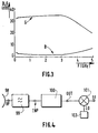
- the amplifier circuit 100 of FIG. 2 shows a flat gain G of approximately 35dB between a few Hz and 3GHz, and a gain of more than 20dB up to 5GHz.
- This circuit shows a noise factor B low and very constant in the same frequency range F.
- FIG. 4 shows a device for radio frequency reception which comprises: a radio frequency filter 99 receiving an RF signal coming from an antenna 98, and connected to the INP input of the amplifier 100; the circuit amplifier 100 having an output marked OUT; and a mixer 101 receiving as input output OUT of amplifier 100 and a signal LO of a local oscillator 102 and providing a output at an IF intermediate frequency.
- a device including such an amplifier circuit 100 shows among other advantages little dispersions depending on the frequency and depending of temperature, and a very constant noise factor.
Landscapes
- Engineering & Computer Science (AREA)
- Power Engineering (AREA)
- Amplifiers (AREA)
Applications Claiming Priority (2)
| Application Number | Priority Date | Filing Date | Title |
|---|---|---|---|
| FR9705670 | 1997-05-07 | ||
| FR9705670A FR2763183A1 (fr) | 1997-05-07 | 1997-05-07 | Dispositif incluant un circuit amplificateur large-bande |
Publications (2)
| Publication Number | Publication Date |
|---|---|
| EP0877478A1 true EP0877478A1 (de) | 1998-11-11 |
| EP0877478B1 EP0877478B1 (de) | 2004-10-06 |
Family
ID=9506697
Family Applications (1)
| Application Number | Title | Priority Date | Filing Date |
|---|---|---|---|
| EP98201374A Expired - Lifetime EP0877478B1 (de) | 1997-05-07 | 1998-04-28 | Vorrichtung mit einer Breitbandverstärkerschaltung |
Country Status (5)
| Country | Link |
|---|---|
| US (1) | US6118991A (de) |
| EP (1) | EP0877478B1 (de) |
| JP (1) | JPH10327025A (de) |
| DE (1) | DE69826759T2 (de) |
| FR (1) | FR2763183A1 (de) |
Families Citing this family (8)
| Publication number | Priority date | Publication date | Assignee | Title |
|---|---|---|---|---|
| US7265618B1 (en) * | 2000-05-04 | 2007-09-04 | Matsushita Electric Industrial Co., Ltd. | RF power amplifier having high power-added efficiency |
| KR100724823B1 (ko) * | 2002-07-26 | 2007-06-04 | 인터내셔널 비지네스 머신즈 코포레이션 | 병렬 피드백 구조물의 다이오드를 이용한 개선된 2 단의큰 대역폭 증폭기 |
| US7787642B2 (en) * | 2003-07-17 | 2010-08-31 | Massachusetts Institute Of Technology | Low-power high-PSRR current-mode microphone pre-amplifier system and method |
| EP1672784B1 (de) * | 2004-12-01 | 2011-05-04 | Alcatel Lucent | Leistungsverstärker |
| US7292097B2 (en) * | 2004-12-10 | 2007-11-06 | Intel Corporation | Amplifier and method for processing signals |
| US9667306B2 (en) * | 2011-10-26 | 2017-05-30 | Adam James Wang | Multimode multiband wireless device with broadband power amplifier |
| US10938360B1 (en) | 2011-10-26 | 2021-03-02 | Micro Mobio Corporation | Multimode multiband wireless device with broadband power amplifier |
| US9948251B2 (en) * | 2016-03-10 | 2018-04-17 | Qorvo Us, Inc. | Low noise amplifier (LNA) system |
Citations (1)
| Publication number | Priority date | Publication date | Assignee | Title |
|---|---|---|---|---|
| EP0161885A2 (de) * | 1984-05-08 | 1985-11-21 | Nec Corporation | Verstärkerschaltung |
Family Cites Families (7)
| Publication number | Priority date | Publication date | Assignee | Title |
|---|---|---|---|---|
| US4071830A (en) * | 1975-07-03 | 1978-01-31 | Motorola, Inc. | Complementary field effect transistor linear amplifier |
| US4647872A (en) * | 1985-07-25 | 1987-03-03 | Johnson William Z | Cascode amplifier |
| US4811424A (en) * | 1987-04-24 | 1989-03-07 | Bell Communications Research, Inc. | Rapid phase correcting carrier recovery circuit |
| US5017884A (en) * | 1989-11-01 | 1991-05-21 | Perandi Aado J | Vacuum tube and MOSFET transimpedance amplifier |
| FR2737065A1 (fr) * | 1995-07-21 | 1997-01-24 | Philips Electronique Lab | Dispositif semiconducteur incluant un amplificateur de puissance et appareil de telecommunication mobile incluant un tel dispositif semiconducteur |
| JP3508401B2 (ja) * | 1996-07-12 | 2004-03-22 | 富士通株式会社 | 増幅回路および多段増幅回路 |
| EP0836275B1 (de) * | 1996-10-11 | 2002-06-05 | STMicroelectronics S.r.l. | Schneller geschalteter Operationsverstärker für Anwendungen bei niedriger Versorgungsspannung |
-
1997
- 1997-05-07 FR FR9705670A patent/FR2763183A1/fr not_active Withdrawn
-
1998
- 1998-04-28 DE DE69826759T patent/DE69826759T2/de not_active Expired - Fee Related
- 1998-04-28 EP EP98201374A patent/EP0877478B1/de not_active Expired - Lifetime
- 1998-05-01 US US09/070,984 patent/US6118991A/en not_active Expired - Fee Related
- 1998-05-06 JP JP10123540A patent/JPH10327025A/ja active Pending
Patent Citations (1)
| Publication number | Priority date | Publication date | Assignee | Title |
|---|---|---|---|---|
| EP0161885A2 (de) * | 1984-05-08 | 1985-11-21 | Nec Corporation | Verstärkerschaltung |
Non-Patent Citations (3)
| Title |
|---|
| FOUQUET F ET AL: "BROADBAND MMIC AMPLIFIER WITH ACTIVE MATCHING", PROCEEDINGS OF THE 23RD. EUROPEAN MICROWAVE CONFERENCE, MADRID, SEPT. 6 - 9, 1993, 6 September 1993 (1993-09-06), EUROPEAN MICROWAVE CONFERENCE MANAGEMENT COMMITTEE, pages 829/830, XP000630008 * |
| J.A. ARCHER ET AL: "A GaAs MONOLITHIC LOW-NOISE BROAD-BAND AMPLIFIER", IEEE JOURNAL OF SOLID-STATE CIRCUITS., vol. sc-16, no. 6, December 1981 (1981-12-01), NEW YORK US, pages 648 - 652, XP002052619 * |
| KENJIRO NISHIKAWA ET AL: "AN MMIC LOW-DISTORTION VARIABLE-GAIN AMPLIFIER USING ACTIVE FEEDBACK", IEEE TRANSACTIONS ON MICROWAVE THEORY AND TECHNIQUES, vol. 43, no. 12, PART 02, 1 December 1995 (1995-12-01), pages 2812 - 2816, XP000549430 * |
Also Published As
| Publication number | Publication date |
|---|---|
| FR2763183A1 (fr) | 1998-11-13 |
| US6118991A (en) | 2000-09-12 |
| JPH10327025A (ja) | 1998-12-08 |
| DE69826759D1 (de) | 2004-11-11 |
| EP0877478B1 (de) | 2004-10-06 |
| DE69826759T2 (de) | 2006-02-23 |
Similar Documents
| Publication | Publication Date | Title |
|---|---|---|
| EP0256580A1 (de) | Gyratorschaltung, die eine Induktanz simuliert | |
| EP0963039B1 (de) | Hochfrequenzvorrichtung mit Leistungsverstärker mit Stabilisierschaltung und mobiles Telefonendgerät mit einer solchen Vorrichtung | |
| FR2612018A1 (fr) | Melangeur hyperfrequences | |
| EP0877478B1 (de) | Vorrichtung mit einer Breitbandverstärkerschaltung | |
| FR3067890B1 (fr) | Architecture de partage de tension entre deux oscillateurs | |
| FR2819652A1 (fr) | Regulateur de tension a rendement ameliore | |
| FR2651936A1 (fr) | Amplificateur a transistor a effet de champ, notamment utilise dans une bande micro-onde. | |
| EP3704793A1 (de) | Verstärker | |
| US6327465B1 (en) | Voltage tunable active inductorless filter | |
| EP0549043B1 (de) | Integrierte Schaltung mit einem Verstärker mit variabler Verstärkung | |
| FR2749718A1 (fr) | Amplificateur a faible bruit | |
| EP0133080B1 (de) | Frequenzunabhängiger Impedanzanpassungsvierpol und Wanderwellenverstärker der diesen verwendet | |
| FR2623951A1 (fr) | Amplificateur lineaire hyperfrequence a tres large bande passante | |
| FR2595173A1 (fr) | Circuit amplificateur distribue large bande dans le domaine des hyperfrequences | |
| EP0387949B1 (de) | Integrierte Halbleitervorrichtung mit einer aktiven Isolatorschaltung | |
| EP1039652B1 (de) | Antenneanordnung | |
| EP1352302A1 (de) | Spannungsregler mit reduzierter statischen verstärkung in offenem regelkreis | |
| EP0500434A1 (de) | Zweifrequenzbereichverstärkermodul | |
| FR2672449A1 (fr) | Dephaseur variable analogique pour signaux hyperfrequence. | |
| FR2578133A1 (fr) | Recepteur autodyne comportant un dispositif d'accord perfectionne | |
| EP1246357A2 (de) | Verstärkervorrichtung mit geschalteter Verstärkung insbesondere für ein mobiles Zelltelephon | |
| FR3047606A1 (fr) | Amplificateur faible bruit entierement integre. | |
| EP0971476B1 (de) | Oszillator mit zwei Quadraturausgängen | |
| US10622960B2 (en) | Filters with virtual inductor implemented using negative capacitor | |
| EP0124940A1 (de) | Phasenriegelschleife und eine solche Schleife enthaltende Anordnung zur Remodulation frequenzmodulierter Signale |
Legal Events
| Date | Code | Title | Description |
|---|---|---|---|
| PUAI | Public reference made under article 153(3) epc to a published international application that has entered the european phase |
Free format text: ORIGINAL CODE: 0009012 |
|
| AK | Designated contracting states |
Kind code of ref document: A1 Designated state(s): DE FR GB |
|
| AX | Request for extension of the european patent |
Free format text: AL;LT;LV;MK;RO;SI |
|
| 17P | Request for examination filed |
Effective date: 19990511 |
|
| AKX | Designation fees paid |
Free format text: DE FR GB |
|
| GRAP | Despatch of communication of intention to grant a patent |
Free format text: ORIGINAL CODE: EPIDOSNIGR1 |
|
| GRAS | Grant fee paid |
Free format text: ORIGINAL CODE: EPIDOSNIGR3 |
|
| GRAA | (expected) grant |
Free format text: ORIGINAL CODE: 0009210 |
|
| AK | Designated contracting states |
Kind code of ref document: B1 Designated state(s): DE FR GB |
|
| REG | Reference to a national code |
Ref country code: GB Ref legal event code: FG4D Free format text: NOT ENGLISH |
|
| REF | Corresponds to: |
Ref document number: 69826759 Country of ref document: DE Date of ref document: 20041111 Kind code of ref document: P |
|
| GBT | Gb: translation of ep patent filed (gb section 77(6)(a)/1977) |
Effective date: 20041210 |
|
| PLBE | No opposition filed within time limit |
Free format text: ORIGINAL CODE: 0009261 |
|
| STAA | Information on the status of an ep patent application or granted ep patent |
Free format text: STATUS: NO OPPOSITION FILED WITHIN TIME LIMIT |
|
| 26N | No opposition filed |
Effective date: 20050707 |
|
| PGFP | Annual fee paid to national office [announced via postgrant information from national office to epo] |
Ref country code: DE Payment date: 20070612 Year of fee payment: 10 |
|
| PGFP | Annual fee paid to national office [announced via postgrant information from national office to epo] |
Ref country code: GB Payment date: 20070425 Year of fee payment: 10 |
|
| PGFP | Annual fee paid to national office [announced via postgrant information from national office to epo] |
Ref country code: FR Payment date: 20070425 Year of fee payment: 10 |
|
| GBPC | Gb: european patent ceased through non-payment of renewal fee |
Effective date: 20080428 |
|
| PG25 | Lapsed in a contracting state [announced via postgrant information from national office to epo] |
Ref country code: DE Free format text: LAPSE BECAUSE OF NON-PAYMENT OF DUE FEES Effective date: 20081101 |
|
| REG | Reference to a national code |
Ref country code: FR Ref legal event code: ST Effective date: 20081231 |
|
| PG25 | Lapsed in a contracting state [announced via postgrant information from national office to epo] |
Ref country code: FR Free format text: LAPSE BECAUSE OF NON-PAYMENT OF DUE FEES Effective date: 20080430 |
|
| PG25 | Lapsed in a contracting state [announced via postgrant information from national office to epo] |
Ref country code: GB Free format text: LAPSE BECAUSE OF NON-PAYMENT OF DUE FEES Effective date: 20080428 |