EP0878773A2 - Tête d'impression avec réseau à diode laser individuellement adressable - Google Patents
Tête d'impression avec réseau à diode laser individuellement adressable Download PDFInfo
- Publication number
- EP0878773A2 EP0878773A2 EP98303343A EP98303343A EP0878773A2 EP 0878773 A2 EP0878773 A2 EP 0878773A2 EP 98303343 A EP98303343 A EP 98303343A EP 98303343 A EP98303343 A EP 98303343A EP 0878773 A2 EP0878773 A2 EP 0878773A2
- Authority
- EP
- European Patent Office
- Prior art keywords
- array
- image
- centerline
- recording surface
- light
- Prior art date
- Legal status (The legal status is an assumption and is not a legal conclusion. Google has not performed a legal analysis and makes no representation as to the accuracy of the status listed.)
- Granted
Links
- 238000003384 imaging method Methods 0.000 claims abstract description 29
- 230000003287 optical effect Effects 0.000 claims abstract description 21
- 238000000034 method Methods 0.000 claims description 9
- 239000013307 optical fiber Substances 0.000 claims description 3
- 230000000694 effects Effects 0.000 description 6
- 239000000835 fiber Substances 0.000 description 5
- 230000004048 modification Effects 0.000 description 3
- 238000012986 modification Methods 0.000 description 3
- 238000004519 manufacturing process Methods 0.000 description 2
- 229910001218 Gallium arsenide Inorganic materials 0.000 description 1
- 206010034960 Photophobia Diseases 0.000 description 1
- 230000004075 alteration Effects 0.000 description 1
- 238000003491 array Methods 0.000 description 1
- 150000001875 compounds Chemical class 0.000 description 1
- 230000007423 decrease Effects 0.000 description 1
- 238000005516 engineering process Methods 0.000 description 1
- 210000003128 head Anatomy 0.000 description 1
- 208000013469 light sensitivity Diseases 0.000 description 1
- 239000003607 modifier Substances 0.000 description 1
- 210000001747 pupil Anatomy 0.000 description 1
- 239000004065 semiconductor Substances 0.000 description 1
Images



Classifications
-
- G—PHYSICS
- G02—OPTICS
- G02B—OPTICAL ELEMENTS, SYSTEMS OR APPARATUS
- G02B13/00—Optical objectives specially designed for the purposes specified below
- G02B13/24—Optical objectives specially designed for the purposes specified below for reproducing or copying at short object distances
-
- B—PERFORMING OPERATIONS; TRANSPORTING
- B41—PRINTING; LINING MACHINES; TYPEWRITERS; STAMPS
- B41J—TYPEWRITERS; SELECTIVE PRINTING MECHANISMS, i.e. MECHANISMS PRINTING OTHERWISE THAN FROM A FORME; CORRECTION OF TYPOGRAPHICAL ERRORS
- B41J2/00—Typewriters or selective printing mechanisms characterised by the printing or marking process for which they are designed
- B41J2/435—Typewriters or selective printing mechanisms characterised by the printing or marking process for which they are designed characterised by selective application of radiation to a printing material or impression-transfer material
- B41J2/447—Typewriters or selective printing mechanisms characterised by the printing or marking process for which they are designed characterised by selective application of radiation to a printing material or impression-transfer material using arrays of radiation sources
- B41J2/45—Typewriters or selective printing mechanisms characterised by the printing or marking process for which they are designed characterised by selective application of radiation to a printing material or impression-transfer material using arrays of radiation sources using light-emitting diode [LED] or laser arrays
- B41J2/451—Special optical means therefor, e.g. lenses, mirrors, focusing means
Definitions
- the present invention relates to a printhead for an electrooptical plotter and, more particularly, to a printhead that produces a multiplicity of light spots on a surface to be plotted, such as that of a printing plate in a plate imagesetter.
- the light from one or more laser sources is focused onto the surface of light sensitive film or plate.
- this surface (whether of a flim or a plate) will be referred to hereunder as the film.
- the plotting rate is generally limited by the power of the laser beam and by the speed at which it can be made to sweep the surface of the film.
- the power limitation is particularly problematic in plate imagesetters, owing to the inherently low light sensitivity of current printing plates.
- it is known to employ a multiplicity of laser sources usually laser diodes (LDs), operating in parallel and producing a multiplicity of traces on the film when scanning it.
- LDs laser diodes
- a practical device for such a purpose is an individually addressable laser diode array (IALDA), which consists of a single bar of semiconducting material, such as GaAs, in which a linear array of addressable lasing sections has been formed. It is noted that such an IALDA device is distinct from a non-addressable laser diode array device, which has been used in imagesetters as a light source to illuminate an array of light modulators.
- IALDA individually addressable laser diode array
- IALDA individually addressable laser diode array
- Such an IALDA device is distinct from a non-addressable laser diode array device, which has been used in imagesetters as a light source to illuminate an array of light modulators.
- the advantages of IALDA over an array of discrete LDs are much lower costs and the closer achievable spacing of the individual lasing sections, although they still cannot be contiguous.
- One possible disadvantage of IALDA is that at high power output any one section may fail, which would render the whole device
- the light emitting region has a very elongated shape, typically 1 micron across and 50 to 200 microns along, and (2) the beam divergence in the cross direction is relatively high - typically 45 degrees FWHM, corresponding to a numerical aperture (NA) of 0.4 - while in the length direction it is relatively low - typically 12 degrees FWHM, corresponding to a NA of 0.1.
- NA numerical aperture
- the light beams emitted by an IALDA device, or a linear array of laser diodes is simply focused by an objective lens onto the film, thus forming on the film an array of projected spots, which is the image of the array of lasing regions, as is illustrated in Fig. 1.
- the film travels in a certain direction 44 , causing the light spots to record parallel traces 46 on the film, as shown.
- the array would be oriented so that the length axis 42 of its image is normal to the direction of travel 44 .
- the device or the array is usually turned, in a plane parallel to the film, so that length axis 42 becomes oriented by an angle ⁇ with respect to the direction nonnal to the direction of travel 44 , and thus traces 46 become closer together.
- the individual laser sources are modulated so that the resultant intensities along each trace 46 vary according to the picture being plotted, the relative timing of modulation among the various sources being adjusted so that resultant features of the picture become properly alligned on the film.
- Angle ⁇ is chosen so that the pitch of the traces, p', assumes a desired value. Ideally, the projected width of each spot, in a direction normal to the trace, is equal to the pitch, p'.
- each LD would be oriented so that the long dimension of each emitting region remains nonnal to trace direction 44 ; angle ⁇ and the projection parameters can then be chosen so that trace contiguity is maintained.
- an LD array device such as an IALDA. the length axis of each lasing region fixedly coincides with the long axis of the array.
- each projected spot forms an angle ⁇ with the nonnal to trace direction 44 and consequently the effective trace width, w', becomes narrower than the actual spot width, w, along its length axis.
- the second characteristic namely the anamorphic beam divergence, may cause a difficulty in designing light efficient projection optics, since the numerical aperture of the objective lens must then be very large. It is noted that usually the length of each projected spot need to be in the range of 10-30 microns and thus - much smaller than the length of each emitting region. This requires the projection optics to effect minification, which further increases the necessary NA on their exit side, if they are to accommodate the entire beam.
- anamorphic projection optics such that have a large numerical aperture in the cross direction only and such that will create an as nearly circular spot image as possible.
- One general configuration of such optics is an afocal arrangement, which consists of a collimating objective lens, or group, a focusing lens, or group, and an anamorphic modification.
- a modification employed, for example, in US Patents 4,520,471 and 4,932,734, is to interject between the two lens groups (which by themselves are generally spherical) a pair of cylindrical lenses that act as a beam expander, or as a modifier of beam expansion, in one axis.
- Another method employed, for example, in US Patents 5,541,951 and 5,594,752 (Figs. 1-3), is to compose the objective assembly out of cylindrical lenses of different powers in each axis.
- the present invention successfully addresses the shortcomings of the presently known configurations by providing a simple and compact optical system for imaging an array of light emitters, such as a laser diodes array, and particularly an individually addressable laser diodes array, onto a recording surface, whereby the image of each emitting region is spread in the cross direction to a width approximately equal to its length dimension.
- an array of light emitters such as a laser diodes array, and particularly an individually addressable laser diodes array
- the present invention discloses a novel optical arrangement, consisting of a main non-anamorphic imaging lens assembly and a single cylindrical lens disposed between the array and the imaging lens assembly, with its focal line parallel to the array's centerline.
- the imaging lens assembly which preferably has a confocal telecentric configuration, focuses the image along the length axis.
- the cylindrical lens is made to form either a real image of the array's centerline (that is - a real image of the array in the transverse axis) in front of the imaging lens assembly or a virtual image of the array's centerline behind the array.
- the array's image will be focused in the transverse axis at a plane behind the recording surface; in the second case, the array's image will be focused in the transverse axis at a plane in front of the recording surface.
- the numerical aperture of the emitted beams in the transverse axis is reduced prior to entry into the imaging lens assembly.
- an optical system for projecting the light emitted from a linear array of light emitting regions within a planar surface, particularly that of an individually addressable laser diodes array device, onto a recording surface, each region having a long axis therethrough that is substantially colinear with the array centerline and a short axis, perpendicular to the long axis, and the dimension of each region along the short axis being substantially smaller than its dimension along the long axis, the system comprising --
- said image is essentially in focus in a direction parallel to the image centerline and is substantially spread in a direction normal to said image centerline.
- the dimension of each of said light spots in a direction normal to said image centerline is essentially equal to the dimension of that light spot in a direction parallel to said image centerline.
- said imaging lens assembly has a telecentric configuration and is non-anamorphic
- said cylindrical lens forms either a real image or a virtual image of the array centerline.
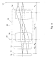
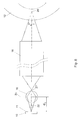
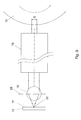
- Figures 2-4 illustrate the general configuration of the optical projection system to project the light emitted from an individually addressable laser diode array device (IALDA) 10 onto a film 12 while the thus projected light spots scan the film.
- the film 12 is wrapped around a rotating drum 14 , as is typical for an external-drum imagesetter, but other configurations are possible too.
- the array consists of a row of lasing sections, spaced by non-lasing sections and ending with light-emitting regions at a plane face 11 .
- Each lasing section is coupled to an individually addressable electrode, to which current is applied from a driver circuit (not shown) according to image signal and accordingly emits light in a beam that is generally centered about a line normal to face 11 .
- Each emitting region is typically about 1 micrometer across and 60 micrometer long and the centerlines of all regions along their long dimensions are substantially colinear with a longitudinal array centerline 24 lying in the plane of emitting face 11 .
- the IALDA is positioned with its emitting face 11 essentially parallel to the section of film being scanned (or written on), at a distance d3 therefrom, and so that a line through the center of the array of emitting regions and normal to face 11 is also normal to that section of film.
- This normal line will be referred to as the optical axis of the (projection) system.
- the array and its centerline 24 are shown, in this example, as being parallel to the rotation axis of the drum, it may be inclined, within a plane normal to the system optical axis, at any angle ⁇ with respect to such a parallel position, in order to effect contiguous scan traces (as explained hereabove with respect to Fig. 1).
- a positive cylindrical lens 16 disposed so that its axial plane includes the optical axis of the system, its principal plane (within the meaning of a thin lens approximation) 25 is parallel to device face 11 and at a distance d1 therefrom and its focal line 22 is parallel to array centerline 24 .
- the cylindrical lens is slightly longer than the array and has preferably a numerical aperture such that it intercepts essentially the entire width of the emitted beams diverging in the cross direction, that is -- in any plane nonnal to centerline 24. As was noted in the background section, this divergence usually forms a relatively large angle - typically 45 degrees FWHM (corresponding to a NA of 0.4).
- cylindrical lens 16 Practically all the light transmitted by cylindrical lens 16 is intercepted by a non-anamorphic imaging lens assembly 18 , which serves to image face 11 , with its light emitting regions, onto film 12 .
- This imaging is done with a demagnification of typically 3, so that each 60 microns long emitting region produces a 20 microns long image.
- the convergence angle of the beams in the cross axis if they fully passed through lens assembly 18 , would have been commensurately larger than 45 degrees, namely, in this case, 140 degrees FWHM (corresponding to a NA of 0.95). This would require imaging lens assembly 18 to have an unrealistically large NA. It is the function of cylindrical lens 16 , inter alia , to reduce the NA of the beams in the cross axis, before entering lens assembly 18 , to a practical value.
- Imaging lens assembly 18 may generally have any positive-acting configuration, preferably consisting of spherical elements and having relatively short conjugate focal distances. It is positioned so that its optical axis is normal to emitting face 11 of the device and centered about the array of emitting regions and so that its principal plane on the entrance side 27 is a distance d2 from face 11 . Distances d2 and d3 are chosen, or adjusted to be, so that the projected image on the surface of film 12 has the desired size and is sharp in the direction parallel to centerline 24 . It is noted that in this direction cylindrical lens 16 has relatively little effect.
- lens 16 decreases the divergence of the beams in the cross direction and, as a result, the images of the emitting regions are focused at a line 28 that is away from the surface of film 12, while at this surface the images are spread in the cross direction by an amounts.
- the distance d1 is preferably chosen, or adjusted to be, so that the spread s is approximately equal to the length dimension of the image.
- the shape of the image of each region is then approximately square and thus practically nears a circular spot.
- a circular spot is desirable, for example, when the array (and its centerline 24 ) must be rotated about the system optical axis by an angle ⁇ , so that the traces of its image become contiguous. The need for a circular spot increases in direct relation to angle ⁇ .
- lens assembly 18 has a confocal telecentric configuration (that is - telecentric towards both the object plane and the image plane), which has the property that the principal ray from any object point enters and exits lens assembly 18 parallel to the optical axis.
- This property carries the advantage that the size of the projected image is insensitive to variations in the distances between the lens assembly and the object- and image planes (variations that could result from mechanical inaccuracies or vibrations).
- Lens assembly 18 can be described as comprising two spherical lens groups - an object group 32 , facing the IALDA and having a focal distance Fo, and an image group 34 , facing the film and having a focal distance Fi.
- Fo 3Fi.
- the distance between the two groups is such that their respective inner foci coincide, at point 36 ; in other words, the distance between their respective principal planes 33 and 35 is equal to Fo+Fi (which, in this case, is 4Fi).
- Fig. 6 which shows the system axial plane that includes array centerline 24
- the principal plane (in the sense of a thin-lens approximation) 33 of object group 32 (which is identical to the entrance principal plane 27 of Fig. 3) is positioned at a distance d2 from emitting face 11 that is equal to Fo
- principal plane 35 of image group 34 is positioned at a distance from film 12 that is equal to Fi.
- distance d2 must be adjusted to account for the effect in the parallel axis of cylindrical lens 16 on the optical path, which is essentially uniform.
- Lens 16 which may generally be a simple lens, a compound lens or even a lens groups, preferably consists of a piece of optical fiber, available from Team Technologies, Auburn, CA.
- the fiber may. have various sizes and cross-sectional shapes and structures; in the present example it has a circular cross-section, with diameter 2R, as illustrated in Fig. 7.
- the value of R is typically in the range of 0.07 to 5 mm. Its focal distance, namely the distance from its front focal line 22 to its principal plane 37 , is approximately equal to R.
- d1 which was defined above as the distance from array centerline 24 to principal plane 25 of lens 16 ) such that the entire width of all the light beam in the cross direction will refract into the entrance pupil of objective group 32 of imaging lens assembly 18 .
- This range extends from a certain value at which focal line 22 is behind array centerline 24 , to a certain value at which focal line 22 is in front of array centerline 24 .
- only a few particular values within this range result in the other desirable effect, namely the widening of the projected spots to become equal to their length dimension.
- d1 is shorter than the focal distance (that is, emitting face 11 is closer to lens 16 than is its focal line 22 ).
- lens 16 produces in the cross direction a virtual image of the array, which lies at a line 26 behind focal line 22 .
- This virtual image serves as a virtual object for lens assembly 18, which projects therefrom a real image onto film 12 .
- this image is in focus at a line 28 , which lies a certain distance in front of the film, while at the plane of the film it is spread out to a dimension s.
- the distance d1 is chosen or adjusted to be such that s is essentially equal to the length dimension of an imaged spot (which, in our example, is 20 microns).
- the parameters of the various lenses are chosen to be such that when this condition is obtained, all light beams fully clear the apertures of all lenses. Another consideration is to minimize spherical aberrations, by keeping the focal length of the cylindrical lens as short as possible. The required calculations can be made by persons knowledgeable in geometric optics.
- d1 is longer than the focal distance of the cylindrical lens (that is, focal line 22 is between lens 16 and emitting face 11 ). so that lens 16 forms in the cross direction a real image of the emitting array at a line 27 between lens 16 and object group 32 , as seen in Fig. 8.
- the distance between lens 16 and image line 27 is made to be large enough for the resultant beam divergence to be within the acceptable range.
- Imaging lens assembly 18 projects line 27 onto the film, but, as is illustrated in Fig. 8, the projected image would be focused at a line 29 behind the film, while at the plane of the film it is spread out to a dimension s. Again, by judicious choice of parameters, the spread s can assume the desired size.
- focal line 22 of lens 16 coincides with array centerline 24 .
- all beams are collimated in the cross direction. They also exit from imaging lens assembly 18 , and hit film 12 , collimated.
- the resultant spots on the film have then a size, in the cross direction, equal to the width of the collimated beams. This width is determined by the emitted divergence angle, ⁇ 1, and by the focal length of lens 16. By proper choice of the latter, the spots can be made to have the desired width s.
- optical projection system of the present invention is relatively simple and that, moreover, it does not require careful alignment beyond the usual axial alignment, the only critical adjustments being those of distance d1 and of distance d2 (or d3); its manufacturing costs should therefore be relatively low.
Landscapes
- Physics & Mathematics (AREA)
- Optics & Photonics (AREA)
- Health & Medical Sciences (AREA)
- General Health & Medical Sciences (AREA)
- Toxicology (AREA)
- General Physics & Mathematics (AREA)
- Printers Or Recording Devices Using Electromagnetic And Radiation Means (AREA)
- Lenses (AREA)
Applications Claiming Priority (2)
| Application Number | Priority Date | Filing Date | Title |
|---|---|---|---|
| IL12084197 | 1997-05-16 | ||
| IL12084197A IL120841A (en) | 1997-05-16 | 1997-05-16 | Writing heads with an array of laser diodes that can be turned separately |
Publications (3)
| Publication Number | Publication Date |
|---|---|
| EP0878773A2 true EP0878773A2 (fr) | 1998-11-18 |
| EP0878773A3 EP0878773A3 (fr) | 1999-09-08 |
| EP0878773B1 EP0878773B1 (fr) | 2002-06-12 |
Family
ID=11070136
Family Applications (1)
| Application Number | Title | Priority Date | Filing Date |
|---|---|---|---|
| EP98303343A Expired - Lifetime EP0878773B1 (fr) | 1997-05-16 | 1998-04-29 | Tête d'impression avec réseau à diode laser individuellement adressable |
Country Status (4)
| Country | Link |
|---|---|
| US (1) | US5986819A (fr) |
| EP (1) | EP0878773B1 (fr) |
| DE (1) | DE69805913T2 (fr) |
| IL (1) | IL120841A (fr) |
Cited By (8)
| Publication number | Priority date | Publication date | Assignee | Title |
|---|---|---|---|---|
| DE10108624A1 (de) * | 2001-02-22 | 2002-09-05 | Heidelberger Druckmasch Ag | Banding-reduzierende Bebilderung einer Druckform |
| DE10233491A1 (de) * | 2002-07-24 | 2004-02-05 | Heidelberger Druckmaschinen Ag | Kompakte Einrichtung zur Bebilderung einer Druckform |
| US6784912B2 (en) | 2000-06-30 | 2004-08-31 | Heidelberger Druckmaschinen Ag | Compact multibeam laser light source and interleaving raster scan line method for exposing printing plates |
| US6900826B2 (en) | 2002-02-19 | 2005-05-31 | Presstek, Inc. | Multiple resolution helical imaging system and method |
| US6919997B2 (en) | 2002-07-24 | 2005-07-19 | Heidelberger Druckmaschinen Ag | Compact device for imaging a printing form |
| DE20023981U1 (de) | 2000-06-30 | 2008-06-19 | Heidelberger Druckmaschinen Ag | Kompakte Mehrstrahllaserlichtquelle zur Belichtung von Druckplatten |
| JP2009067041A (ja) * | 2007-08-20 | 2009-04-02 | Seiko Epson Corp | ラインヘッド及びそれを用いた画像形成装置 |
| EP2020293A3 (fr) * | 2007-07-31 | 2009-08-12 | Seiko Epson Corporation | Tête à fil et appareil d'imagerie l'incorporant |
Families Citing this family (20)
| Publication number | Priority date | Publication date | Assignee | Title |
|---|---|---|---|---|
| US6348358B1 (en) | 1999-02-19 | 2002-02-19 | Presstek, Inc. | Emitter array with individually addressable laser diodes |
| US6480219B1 (en) * | 1999-07-21 | 2002-11-12 | Fuji Photo Film Co., Ltd. | Exposure head |
| US20020149665A1 (en) | 2000-07-03 | 2002-10-17 | Serge Steinblatt | Redundancy for individually addresable laser diode arrays based systems |
| US6433934B1 (en) | 2000-08-11 | 2002-08-13 | Yakov Reznichenko | Illumination system for use in imaging systems |
| US6603498B1 (en) | 2000-11-28 | 2003-08-05 | Coherent, Inc. | Printer head with linear array of individually addressable diode-lasers |
| US6646669B2 (en) | 2000-12-14 | 2003-11-11 | Creo Inc. | Multimode multi-track optical recording system |
| US6661587B2 (en) | 2002-02-26 | 2003-12-09 | Richard G. Smith | Confocal optical design for optical coupling |
| US7066088B2 (en) * | 2002-07-31 | 2006-06-27 | Day International, Inc. | Variable cut-off offset press system and method of operation |
| US8570356B2 (en) * | 2009-06-03 | 2013-10-29 | John Michael Tamkin | Optical system for direct imaging of light markable material |
| US9347642B2 (en) | 2011-09-07 | 2016-05-24 | Terralux, Inc. | Faceted optics for illumination devices |
| US9470406B2 (en) | 2012-09-24 | 2016-10-18 | Terralux, Inc. | Variable-beam light source and related methods |
| CA2917772A1 (fr) | 2013-07-09 | 2015-01-15 | Terralux, Inc. | Source de lumiere a faisceau variable et procedes associes |
| CN103513664B (zh) * | 2013-09-22 | 2015-10-28 | 济南大学 | 小孔测量中传感器的自动对中系统 |
| US10072819B2 (en) | 2014-10-02 | 2018-09-11 | Ledvance Llc | Light source for uniform illumination of a surface |
| US10036535B2 (en) | 2014-11-03 | 2018-07-31 | Ledvance Llc | Illumination device with adjustable curved reflector portions |
| US10405388B2 (en) | 2014-12-11 | 2019-09-03 | Ledvance Llc | Variable-beam light source with mixing chamber |
| KR102035316B1 (ko) * | 2017-10-25 | 2019-10-22 | 주식회사 루트로닉 | 치료용 레이저 장치 |
| US12030251B2 (en) | 2021-08-20 | 2024-07-09 | General Electric Company | Irradiation devices with optical modulators for additively manufacturing three-dimensional objects |
| US12017298B2 (en) | 2021-08-20 | 2024-06-25 | General Electric Company | Irradiation devices with optical modulators for additively manufacturing three-dimensional objects |
| US12558846B2 (en) | 2023-03-06 | 2026-02-24 | General Electric Company | Irradiation devices with optical modulators for additively manufacturing three-dimensional objects |
Family Cites Families (13)
| Publication number | Priority date | Publication date | Assignee | Title |
|---|---|---|---|---|
| FR2365750A1 (fr) * | 1976-09-24 | 1978-04-21 | Thomson Csf | Support de positionnement pour fibres optiques |
| US4474422A (en) * | 1979-11-13 | 1984-10-02 | Canon Kabushiki Kaisha | Optical scanning apparatus having an array of light sources |
| US4520471A (en) * | 1983-02-07 | 1985-05-28 | Rca Corporation | Multi-channel recording/playback optics for laser diode arrays |
| US4520472A (en) * | 1983-02-07 | 1985-05-28 | Rca Corporation | Beam expansion and relay optics for laser diode array |
| JP2741195B2 (ja) * | 1987-02-25 | 1998-04-15 | 株式会社 リコー | レーザーダイオードアレイを用いる光走査光学系 |
| JP2554724B2 (ja) * | 1987-12-11 | 1996-11-13 | 株式会社リコー | レーザーダイオードアレイを用いる光走査光学系 |
| US5168288A (en) * | 1989-12-18 | 1992-12-01 | Eastman Kodak Company | Thermal a scan laser printer |
| CA2077813C (fr) * | 1991-12-20 | 1998-07-28 | Thomas L. Paoli | Dispositif et methode de commande de la position du spot dans un appareil de sortie utilisant un reseau lineaire de sources lumineuses |
| US5745153A (en) * | 1992-12-07 | 1998-04-28 | Eastman Kodak Company | Optical means for using diode laser arrays in laser multibeam printers and recorders |
| JPH0727988A (ja) * | 1993-07-08 | 1995-01-31 | Canon Inc | 光走査装置 |
| US5521748A (en) * | 1994-06-16 | 1996-05-28 | Eastman Kodak Company | Light modulator with a laser or laser array for exposing image data |
| US5541951A (en) * | 1994-11-14 | 1996-07-30 | Intelligent Surgical Lasers, Inc. | Device and method for high-power end pumping |
| JPH10278345A (ja) * | 1997-04-10 | 1998-10-20 | Dainippon Screen Mfg Co Ltd | 画像記録装置 |
-
1997
- 1997-05-16 IL IL12084197A patent/IL120841A/en not_active IP Right Cessation
-
1998
- 1998-04-23 US US09/064,741 patent/US5986819A/en not_active Expired - Lifetime
- 1998-04-29 EP EP98303343A patent/EP0878773B1/fr not_active Expired - Lifetime
- 1998-04-29 DE DE69805913T patent/DE69805913T2/de not_active Expired - Lifetime
Cited By (11)
| Publication number | Priority date | Publication date | Assignee | Title |
|---|---|---|---|---|
| US6784912B2 (en) | 2000-06-30 | 2004-08-31 | Heidelberger Druckmaschinen Ag | Compact multibeam laser light source and interleaving raster scan line method for exposing printing plates |
| US7330203B2 (en) | 2000-06-30 | 2008-02-12 | Heidelberger Druckmaschinen Ag | Compact multibeam laser light source and interleaving raster scan |
| DE20023981U1 (de) | 2000-06-30 | 2008-06-19 | Heidelberger Druckmaschinen Ag | Kompakte Mehrstrahllaserlichtquelle zur Belichtung von Druckplatten |
| DE10108624A1 (de) * | 2001-02-22 | 2002-09-05 | Heidelberger Druckmasch Ag | Banding-reduzierende Bebilderung einer Druckform |
| US6765604B2 (en) | 2001-02-22 | 2004-07-20 | Heidelberger Druckmaschinen Ag | Banding-reduced imaging of a printing form |
| US6900826B2 (en) | 2002-02-19 | 2005-05-31 | Presstek, Inc. | Multiple resolution helical imaging system and method |
| DE10233491A1 (de) * | 2002-07-24 | 2004-02-05 | Heidelberger Druckmaschinen Ag | Kompakte Einrichtung zur Bebilderung einer Druckform |
| US6919997B2 (en) | 2002-07-24 | 2005-07-19 | Heidelberger Druckmaschinen Ag | Compact device for imaging a printing form |
| DE10233491B4 (de) * | 2002-07-24 | 2012-12-20 | Heidelberger Druckmaschinen Ag | Kompakte Einrichtung zur Bebilderung einer Druckform |
| EP2020293A3 (fr) * | 2007-07-31 | 2009-08-12 | Seiko Epson Corporation | Tête à fil et appareil d'imagerie l'incorporant |
| JP2009067041A (ja) * | 2007-08-20 | 2009-04-02 | Seiko Epson Corp | ラインヘッド及びそれを用いた画像形成装置 |
Also Published As
| Publication number | Publication date |
|---|---|
| EP0878773B1 (fr) | 2002-06-12 |
| US5986819A (en) | 1999-11-16 |
| DE69805913D1 (de) | 2002-07-18 |
| EP0878773A3 (fr) | 1999-09-08 |
| IL120841A0 (en) | 1997-09-30 |
| IL120841A (en) | 2001-07-24 |
| DE69805913T2 (de) | 2003-01-23 |
Similar Documents
| Publication | Publication Date | Title |
|---|---|---|
| EP0878773B1 (fr) | Tête d'impression avec réseau à diode laser individuellement adressable | |
| US4390235A (en) | Multibeam scanning apparatus provided with a function of changing magnification | |
| US4474422A (en) | Optical scanning apparatus having an array of light sources | |
| US5995475A (en) | Two dimensional laser diode array using multimode lasers | |
| CA2375419A1 (fr) | Dispositif d'enregistrement d'images pour forme d'impression, dote d'un reseau de sources lumineuses vcsel | |
| US5463418A (en) | Plural-beam scanning optical apparatus | |
| JPH0679920A (ja) | 多重ダイオードレーザを使用する印刷システム | |
| US5510826A (en) | Optical scanning apparatus | |
| US4571021A (en) | Plural-beam scanning apparatus | |
| US5818645A (en) | Multimode optical source and image scanning apparatus using the same | |
| US5028103A (en) | Optical scanning apparatus | |
| KR19980019037A (ko) | 멀티-빔 주사장치(multi-beam scanning apparatus with controlled scan line bow) | |
| JPH1114923A (ja) | 光学走査装置 | |
| US5008686A (en) | Optical scanning device for scanning a predetermined surface with a plurality of light beams | |
| US4641950A (en) | Exposure system | |
| JP3197804B2 (ja) | マルチビーム走査装置 | |
| JPH09304720A (ja) | 光学走査装置及び光学レンズ | |
| US5278691A (en) | Symmetrical overfilled polygon laser scanner | |
| JPH0618802A (ja) | 光走査装置 | |
| JP2004087816A (ja) | 光源装置および画像記録装置 | |
| JP2741195B2 (ja) | レーザーダイオードアレイを用いる光走査光学系 | |
| US5671004A (en) | Internal drum scanning type image recording apparatus | |
| JPS6410805B2 (fr) | ||
| JPH05259580A (ja) | 光源ユニット | |
| JP2811988B2 (ja) | 画像形成装置における光走査装置 |
Legal Events
| Date | Code | Title | Description |
|---|---|---|---|
| PUAI | Public reference made under article 153(3) epc to a published international application that has entered the european phase |
Free format text: ORIGINAL CODE: 0009012 |
|
| AK | Designated contracting states |
Kind code of ref document: A2 Designated state(s): BE DE FR GB |
|
| AX | Request for extension of the european patent |
Free format text: AL;LT;LV;MK;RO;SI |
|
| PUAL | Search report despatched |
Free format text: ORIGINAL CODE: 0009013 |
|
| RIC1 | Information provided on ipc code assigned before grant |
Free format text: 6G 06K 15/12 A, 6H 04N 1/191 B, 6G 02B 27/09 B, 6B 41J 2/45 B |
|
| AK | Designated contracting states |
Kind code of ref document: A3 Designated state(s): AT BE CH CY DE DK ES FI FR GB GR IE IT LI LU MC NL PT SE |
|
| AX | Request for extension of the european patent |
Free format text: AL;LT;LV;MK;RO;SI |
|
| 17P | Request for examination filed |
Effective date: 19991103 |
|
| 17Q | First examination report despatched |
Effective date: 20000222 |
|
| AKX | Designation fees paid |
Free format text: BE DE FR GB |
|
| RAP1 | Party data changed (applicant data changed or rights of an application transferred) |
Owner name: CREOSCITEX CORPORATION LTD. |
|
| GRAG | Despatch of communication of intention to grant |
Free format text: ORIGINAL CODE: EPIDOS AGRA |
|
| GRAG | Despatch of communication of intention to grant |
Free format text: ORIGINAL CODE: EPIDOS AGRA |
|
| GRAH | Despatch of communication of intention to grant a patent |
Free format text: ORIGINAL CODE: EPIDOS IGRA |
|
| GRAH | Despatch of communication of intention to grant a patent |
Free format text: ORIGINAL CODE: EPIDOS IGRA |
|
| GRAA | (expected) grant |
Free format text: ORIGINAL CODE: 0009210 |
|
| AK | Designated contracting states |
Kind code of ref document: B1 Designated state(s): BE DE FR GB |
|
| RAP1 | Party data changed (applicant data changed or rights of an application transferred) |
Owner name: CREO IL. LTD. |
|
| REG | Reference to a national code |
Ref country code: GB Ref legal event code: FG4D |
|
| REF | Corresponds to: |
Ref document number: 69805913 Country of ref document: DE Date of ref document: 20020718 |
|
| ET | Fr: translation filed | ||
| PLBE | No opposition filed within time limit |
Free format text: ORIGINAL CODE: 0009261 |
|
| STAA | Information on the status of an ep patent application or granted ep patent |
Free format text: STATUS: NO OPPOSITION FILED WITHIN TIME LIMIT |
|
| PG25 | Lapsed in a contracting state [announced via postgrant information from national office to epo] |
Ref country code: BE Free format text: LAPSE BECAUSE OF NON-PAYMENT OF DUE FEES Effective date: 20030430 |
|
| 26N | No opposition filed |
Effective date: 20030313 |
|
| BERE | Be: lapsed |
Owner name: *CREO IL. LTD Effective date: 20030430 |
|
| PG25 | Lapsed in a contracting state [announced via postgrant information from national office to epo] |
Ref country code: FR Free format text: LAPSE BECAUSE OF NON-PAYMENT OF DUE FEES Effective date: 20031231 |
|
| REG | Reference to a national code |
Ref country code: FR Ref legal event code: ST |
|
| PGFP | Annual fee paid to national office [announced via postgrant information from national office to epo] |
Ref country code: GB Payment date: 20120327 Year of fee payment: 15 |
|
| PGFP | Annual fee paid to national office [announced via postgrant information from national office to epo] |
Ref country code: DE Payment date: 20120430 Year of fee payment: 15 |
|
| GBPC | Gb: european patent ceased through non-payment of renewal fee |
Effective date: 20130429 |
|
| PG25 | Lapsed in a contracting state [announced via postgrant information from national office to epo] |
Ref country code: DE Free format text: LAPSE BECAUSE OF NON-PAYMENT OF DUE FEES Effective date: 20131101 Ref country code: GB Free format text: LAPSE BECAUSE OF NON-PAYMENT OF DUE FEES Effective date: 20130429 |
|
| REG | Reference to a national code |
Ref country code: DE Ref legal event code: R119 Ref document number: 69805913 Country of ref document: DE Effective date: 20131101 |