EP0878836B1 - Planarisierung von einem Halbleitersubstrat - Google Patents
Planarisierung von einem Halbleitersubstrat Download PDFInfo
- Publication number
- EP0878836B1 EP0878836B1 EP98303917A EP98303917A EP0878836B1 EP 0878836 B1 EP0878836 B1 EP 0878836B1 EP 98303917 A EP98303917 A EP 98303917A EP 98303917 A EP98303917 A EP 98303917A EP 0878836 B1 EP0878836 B1 EP 0878836B1
- Authority
- EP
- European Patent Office
- Prior art keywords
- insulating layer
- layer
- substrate
- portions
- region
- Prior art date
- Legal status (The legal status is an assumption and is not a legal conclusion. Google has not performed a legal analysis and makes no representation as to the accuracy of the status listed.)
- Expired - Lifetime
Links
Images


Classifications
-
- H—ELECTRICITY
- H10—SEMICONDUCTOR DEVICES; ELECTRIC SOLID-STATE DEVICES NOT OTHERWISE PROVIDED FOR
- H10P—GENERIC PROCESSES OR APPARATUS FOR THE MANUFACTURE OR TREATMENT OF DEVICES COVERED BY CLASS H10
- H10P50/00—Etching of wafers, substrates or parts of devices
-
- H—ELECTRICITY
- H10—SEMICONDUCTOR DEVICES; ELECTRIC SOLID-STATE DEVICES NOT OTHERWISE PROVIDED FOR
- H10P—GENERIC PROCESSES OR APPARATUS FOR THE MANUFACTURE OR TREATMENT OF DEVICES COVERED BY CLASS H10
- H10P95/00—Generic processes or apparatus for manufacture or treatments not covered by the other groups of this subclass
- H10P95/06—Planarisation of inorganic insulating materials
- H10P95/062—Planarisation of inorganic insulating materials involving a dielectric removal step
- H10P95/064—Planarisation of inorganic insulating materials involving a dielectric removal step the removal being chemical etching
Definitions
- the present invention relates to a method for planarising a substrate such as a semiconductor substrate.
- planarisation processes for planarising the surface of the device between formation of the various layers required. Examples include planarising an interlayer insulating layer formed on a semiconductor substrate. Recently, STI (Shallow Trench Isolation) processes have become widely used to electrically isolate device elements on a semiconductor substrate. Compared to the former LOCOS process, a step height between a trench and adjacent device elements is increased, and requires improved planarisation techniques.
- STI Shallow Trench Isolation
- CMP Chemical Mechanical Polishing
- substrate planarisation using CMP leads to three main problems: first, when large areas are to be planarised, a dish-shape is formed in the surface. Second, the substrate may be contaminated by the slurry used. Third, the substrate and the polishing apparatus may be contaminated by particles generated during the CMP.
- US 5,541,427 and US 5,266,525 describe a substrate having a planarised upper surface and comprising elevated and a recessed regions.
- a first insulating layer is provided on the elevated and recessed regions and a portion of a second insulating layer overlies the first insulating layer in the recessed regions.
- a third insulating layer fills the recess to a level substantially coplanar with the first insulating layer. Parts of the second insulating layer are exposed at the planarised upper surface.
- the present invention is intended to address the above problems, by providing a method for efficiently planarising a substrate which does not involve polishing.
- a method for planarising a substrate comprising the steps of: (a) preparing a substrate having an uneven topography, including an elevated region and an adjacent recessed region; (b) forming a first insulating layer on the elevated region and the recessed region; (c) forming a second insulating layer on the first insulating layer; (d) removing portions of the second insulating layer at an interface between the elevated region and the recessed region, to isolate a portion of the second insulating layer within the recessed region from a portion of second insulating layer overlying the elevated region; (e) forming a third insulating layer on the resultant surface; (f) partially removing the third insulating layer from its upper surface until a part of the portion of second insulating layer overlying the elevated region is exposed; and(g) removing the portion of second insulating layer overlying the elevated region, causing lift-off of corresponding portions of the third insulating layer.
- steps (f) and (g) are performed in a single etch process, the conditions of such process being selected such that the second insulating layer is etched at a faster rate than the third insulating layer or the first insulating layer.
- Such an etch process is preferably selected to completely remove the portion of second insulating layer overlying the elevated region before the portion of the second insulating layer within the recessed region is exposed by removal of an overlying part of the third insulating layer.
- Preferred examples of an etch process for use in step (f) and/or step (g) are wet etching, using a solution of hydrogen fluoride HF; alternatively wet etching, using SC1(NH 3 + H 2 O 2 + water) .
- An underlying portion of the first insulating layer is preferably partially removed during, or subsequent to, the step (d).
- the step (d) and the step of partially removing an underlying portion of the first insulating layer may be performed by a sputtering process using argon gas.
- Steps (c) and (d) are preferably concurrently performed.
- the second insulating layer is deposited and at the same time etched, and portions of the second insulating layer at the interface are etched faster than other portions of the second insulating layer. Underlying portions of the first insulating layer at the interface are thereby exposed.
- a substrate having a planarised upper surface comprising an elevated region and an adjacent recessed region, a first insulating layer on the elevated region and the recessed region, a portion of a second insulating layer overlying the first insulating layer within the recessed region and a third insulating layer filling the recessed region to a level substantially coplanar with an upper surface of the first insulating layer, characterised in that the third insulating layer encloses the portion of the second insulating layer within the recessed region whereby no part of the second insulating layer is exposed to the planarised upper surfaces.
- the elevated region may comprise a patterned layer applied to the substrate, and the recessed region may comprise the substrate between elements of the patterned layer.
- the patterned layer may comprise an intermetal dielectric layer, or a metal interconnect layer.
- the elevated region may comprise the substrate, and the recessed region may comprise a trench within the substrate.
- the second layer is composed of one of the group consisting of SiOF, PSG, BN and BPSG.
- the third layer is composed of one of the group consisting of HDP CVD oxide and ECR CVD oxide.
- the substrate may be a semiconductor substrate.
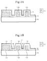
- Figs. 1A to 1F show a method for planarising a semiconductor substrate according to a first embodiment of the present invention.
- a patterned layer 12 of, for example, metal interconnections 12a, 12b and 12c is formed on a semiconductor substrate 10.
- the metal interconnections may have different sizes.
- the semiconductor substrate 10 accordingly has an uneven topography, including an elevated region (metal interconnections) and an adjacent recessed region (spaces between metal interconnections).
- a first insulating layer 14 is formed over the semiconductor substrate 10 including the interconnections 12a, 12b and 12c.
- a second insulating layer 16 is then formed over the first insulating layer.
- the second insulating layer may be composed of SiOF, PSG (Phosphorus Silicate Glass), BN (Boron Nitride), or BPSG (Boron Phosphorus Silicate Glass).
- the second insulating layer has a high etch selectivity with respect to the first insulating layer 14.
- the elevated region may comprise a patterned intermetal dielectric instead of metal interconnections.
- the elevated region may comprise any patterned layer. Examples include polysilicon or other gate layers for transistors, or resistive lines.
- the recessed region may be the substrate 10 between elements 12a, 12b, 12c, of the patterned layer.
- a sputtering process using argon (Ar) gas is performed until portions of the second insulating layer 16 at interfaces between the elevated regions and the recessed regions are removed. The portions of the second insulating layer within the recessed regions is thereby isolated from portions of the second insulating layer overlying the elevated regions.
- Ar argon
- Underlying portions of the first insulating layer 14 at the interfaces are preferably also partially removed. By partially removing the underlying portions of the first isolation layer, the profile of the resulting cavity 17 is rounded at its upper edges. This assists the later filling of the cavity 17.
- a third insulating layer 18 is formed over the resultant surface of the substrate.
- the third insulating layer 18 should preferably be sufficiently thick to fill cavities 17 to at least the level of the upper surface of surrounding portions of the second insulating layer.
- the third insulating layer may be composed of silicon oxide (SiO 2 ) and be formed by a CVD (Chemical Vapour Deposition) process, such as an HDP (High Density Plasma) process, or an ECR (Electron Cyclotron Resonance) process.
- the second insulating layer 16 must be highly selectively etchable with respect to the third insulating layer 18.
- deposition and etching may be simultaneously performed.
- the metal interconnection 12a having a large pattern size becomes coated with a thick third insulating layer portion 18a, having a large step height from the level of the second insulating layer.
- the metal interconnections 12b and 12c become coated with thinner portions 18b, 18c of the third insulating layer on top of corresponding portions of the second insulating layer.
- Figs. 1D to 1F show an etching process for planarising the insulating layers.
- an etching, such as a wet etching, of the third insulating layer 18 is performed until end parts of the second insulating layer 16 overlying the elevated region at the interfaces are exposed.
- the etching continues, and the exposed parts of second insulating layer 16 are etched much faster than the third insulating layer 18 and exposed parts of first insulating layer 14.
- the materials used for the insulating layers, and the conditions used for the etching are chosen such that the second insulating layer 16 may be completely removed from under the remaining portions of the third insulating layer, without etching the third insulating layer within cavities 17 so far that the portions of the second layer within the cavities 17 are exposed.
- the etch conditions used for initially etching the third insulating layer, and those used for etching the second insulating layer when it is exposed, may be the same, or different.
- the second insulating layer 16 is removed much faster than the third insulating layer. This is because the second insulating layer 16 is selected to have a relatively high etch rate compared to the etch rates of the first and third insulating layers 14 and 18, with the chosen etch conditions. In addition, since the second insulating layer 16 is relatively thin compared to the first and third insulating layers, it can be removed far faster, as is apparent from Fig. 1E.
- Figure 1E shows the structure after complete removal of the second and third layers from above the elevated regions corresponding to metal interconnections 12b and 12c.
- the portions of the second insulating layer formed above the metal interconnections 12b and 12c are far narrower than those formed above the metal interconnection 12a.
- the portions of the third insulating layer formed above the metal interconnections 12b and 12c are thinner than those formed above the metal interconnection 12a, as shown by FIG. 1C. Accordingly, the portions of both second and third insulating layers formed above metal interconnections 12b, 12c may all be completely removed by the etch applied.
- the parts of the second and third insulating layers formed above the metal interconnection 12a are significantly wider, and thicker, respectively, and are only partially removed by the etching.
- the portion of the second insulating layer formed above the metal interconnection 12a continues to be removed, while exposed parts of first and third insulating layers are removed only slowly, if at all.
- the third insulating layer 18 formed above the metal interconnection 12a is not completely removed, the second insulating layer 16 is removed from underneath.
- Removal of the second insulating layer 16 causes lift-off of overlying portions 18a of the third insulating layer 18.
- Parts of the third insulating layer within cavities 17, and exposed parts of first insulating layer 14 are only slowly removed. Removal of third and first insulating layers is preferably reduced as much as possible.
- the overlying portions of the third insulating layer are lifted off, the upper surfaces of the portions of the third insulating layer lying within cavities 17 are substantially coplanar with the upper surface of surrounding portions if the first insulating layer 14, overlying the elevated regions.
- the substrate thereby acquires a planarised upper surface, largely corresponding to the original upper surface of the first insulating layer over elevated regions.
- a semiconductor substrate 100 includes a trench 120 formed in its upper surface to define a device isolation region (in this case a trench isolation region). Accordingly, the semiconductor substrate 100 has an upper surface with uneven topography including an elevated region (e.g. the semiconductor substrate regions 100a and 100c adjacent to the trench 120) and an adjacent recessed region 100b (e.g. the trench 120).
- An insulating material is to be placed in the trench, and the upper surface of the filled trench, when completed, should be as planar as possible, coplanar with the surrounding upper surface of the substrate.
- a first insulating layer 140 is formed on both sidewalls and the bottom of the trench 120, 100b and on the upper surface of the elevated regions 100a, 100c.
- a second insulating layer 160 is formed on the first insulating layer 140.
- the second insulating layer 160 may be composed of SiOF, PSG, BN, or BPSG, and has a high etch selectivity with respect to the first insulating layer 140.
- an etching process such as a sputtering process using argon (Ar) gas is performed until portions of the second insulating layer 160 at interfaces between the elevated regions and the recessed regions are removed. The portion of the second insulating layer within the recessed region is thereby isolated from portions of the second insulating layer overlying the elevated regions.
- Ar argon
- Underlying portions of the first insulating layer 140 at the interfaces are preferably also partially removed. By partially removing the underlying portions of the first isolation layer, the profile of the resulting cavity 170 is rounded at its upper edges. This assists the later filling of the cavity 170.
- a third insulating layer 180 for example composed of silicon oxide, is formed over the substrate.
- a suitable process may be a CVD process such as an HDP CVD process or an ECR CVD process.
- the third insulating layer 180 has a high etch selectivity with respect to the second insulating layer 160.
- the third insulating layer 180 should preferably be sufficiently thick to fill trench 120 to at least the level of the upper surface of the surrounding portions of the second insulating layer.
- wide and thick portions 180a, 180c are formed on the elevated regions 100a and 100c, which are large in area.
- On the recessed region 100b, in the trench 120 is formed a part 180b of the third insulating layer, which is thin at upper edges of the trench 120, at interfaces between recessed region 100b and adjacent elevated regions 100a, 100c.
- deposition and etching may be simultaneously performed.
- an etching step such as a wet etching step, is performed to planarise the insulating layers.
- etching of the third insulating layer 180 is performed until end parts of the portions of the second insulating layer 160 overlying the elevated regions are exposed, at an interface between the elevated regions and the recessed region.
- the exposed parts of second insulating layer 160 are etched much faster than exposed parts of the first and third insulating layers 140, 180.
- the second insulating layer 160 may be removed much faster than the third insulating layer. This is because the second insulating layer 160 has a relatively high etch rate compared to that of the first and third insulating layers 140 and 180, under the selected etch conditions. The second insulating layer 160 is also removed faster than the first and third insulating layers because it is relatively thin.
- the portions 180a, 180c of the third insulating layer formed above the elevated regions 100a and 100c are not completely removed during the etching.
- the portions of the second insulating layer formed on the elevated regions continue to be removed, while exposed parts of first 140 and third 180 insulating layers are removed only slowly, if at all.
- the third insulating layer 180a, 180c formed above the elevated regions 100a, 100c is not completely removed, the second insulating layer 160 is removed from underneath.
- Removal of the second insulating layer 160 causes lift-off of overlying portions 180a, 180c of the third insulating layer 180. Removal of third and first insulating layers is preferably reduced as much as possible. When the overlying portions 180a, 180c of the third insulating layer 180 are lifted off, the upper surface of the portion 180b of the third insulating layer lying within trench 120 is substantially coplanar with the upper surface of surrounding portions of the first insulating layer 140 overlying the elevated regions.
- the substrate thereby acquires a planarised upper surface, largely corresponding to the original upper surface of the first insulating layer 140.
- the above-described first, second and third insulating layers may be formed by HDP CVD process or ECR CVD process, in which case, use of the argon sputtering process is unnecessary.
- the second insulating layer is preferably made of material having a relatively high etch selectivity to the materials of the first and third insulating layers.
- the second insulating layer may be composed of a material such as SiOF, PSG, BN or BPSG.
- the third insulating layer may be made of HDP CVD oxide or ECR CVD oxide.
- the present invention provides a method for planarising a substrate with a planarised upper surface by etching, without the dishing phenomenon or contamination by slurry or particles.
- planarising etch in the method according to the invention, using the materials described above for the insulating layers, are as follows.
- the planarising etch must partially remove the third insulating layer from its upper surface and then remove the portion of second insulating layer overlying the elevated region, causing lift-off of corresponding portions of the third insulating layer.
- a suitable etch process is a wet etch using a solution of HF (hydrogen fluoride), in which case the relative etch rates of the first, second and third insulating layers are in the ratio 1:3:0.8, respectively.
- HF hydrogen fluoride
- a wet etch process using SC1 (ammonia NH 3 + hydrogen peroxide H 2 O 2 + deionised water) as an etchant may be used, in which case the relative etch rates of the first, second and third insulating layers are in the ratio 1:7:12, respectively.
- SOI silicon on insulator
- the invention may be applied to the planarisation of any combination of adjacent recessed and elevated regions.
- each of several layers of metal interconnections in a semiconductor integrated circuit may be planarised according to the method of the present invention.
- any suitable materials may be used for the first, second and third insulating layers, provided that the second insulating layer may be preferentially etched with respect to the first and third insulating layers.
- any suitable method may be used to selectively remove the second insulating layer, after partial removal of the third insulating layer.
- a reactive ion etching (RIE) or other dry etching process may be used.
Landscapes
- Internal Circuitry In Semiconductor Integrated Circuit Devices (AREA)
- Element Separation (AREA)
- Formation Of Insulating Films (AREA)
- Drying Of Semiconductors (AREA)
Claims (15)
- Verfahren zur Planarisierung eines Substrats, das die folgenden Schritte umfasst:(a) Erzeugen eines Substrats (10; 100) mit einer Oberseite mit unregelmäßiger Topographie, einschließlich einer erhabenen Region (12; 100a) und einer benachbarten eingetieften Region (17; 100b);(b) Ausbilden einer ersten Isolierschicht (14; 140) auf der erhabenen Region und der eingetieften Region;(c) Ausbilden einer zweiten Isolierschicht (16; 160) auf der ersten Isolierschicht;(d) Entfernen von Abschnitten der zweiten Isolierschicht an einer Grenzfläche zwischen der erhabenen Region und der eingetieften Region, um einen Abschnitt der zweiten Isolierschicht innerhalb der eingetieften Region gegen einen Teil der zweiten Isolierschicht, die über der erhabenen Region liegt, zu isolieren;(e) Ausbilden einer dritten Isolierschicht (18; 180) auf der resultierenden Oberfläche;(f) teilweises Entfernen der dritten Isolierschicht von der Oberseite, bis ein Teil des Abschnitts der zweiten Isolierschicht, die über der erhabenen Region liegt, freigelegt ist; und(g) Entfernen des Abschnitts der zweiten Isolierschicht, der über der erhabenen Region liegt, wodurch eine Abhebung entsprechender Abschnitte (18a, 180a) der dritten Isolierschicht bewirkt wird.
- Verfahren nach Anspruch 1, wobei die Schritte (f) und (g) in einem einzigen Ätzschritt durchgeführt werden, der so ausgewählt wird, dass die zweite Isolierschicht mit einer höheren Rate geätzt wird als die dritte Isolierschicht oder die erste Isolierschicht.
- Verfahren nach Anspruch 2, wobei der Ätzschritt so gewählt wird, dass der Abschnitt der zweiten Isolierschicht, der über der erhabenen Region liegt, vollständig entfernt wird, bevor der Abschnitt der zweiten Isolierschicht innerhalb der eingetieften Region freigelegt wird.
- Verfahren nach einem der vorangehenden Ansprüche, wobei während dem oder im Anschluss an den Schritt (d) ein darunter liegender Abschnitt der ersten Isolierschicht teilweise entfernt wird.
- Verfahren nach Anspruch 4, wobei der Schritt (d) und der Schritt, in dem ein darunter liegender Abschnitt der ersten Isolierschicht teilweise entfernt wird, durch ein Sputter-Verfahren unter Verwendung von Argongas durchgeführt werden.
- Verfahren nach Anspruch 1, wobei die Schritte (c) und (d) gleichzeitig durchgeführt werden, wobei die zweite Isolierschicht abgeschieden und gleichzeitig geätzt wird, um die Abschnitte der zweiten Isolierschicht an der Grenzfläche schneller zu ätzen als andere Abschnitte der zweiten Isolierschicht, und um darunter liegende Abschnitte der ersten Isolierschicht an der Grenzfläche freizulegen.
- Verfahren nach Anspruch 6, wobei die zweite Isolierschicht in einem HDP CVD-Verfahren oder einem ECR CVD-Verfahren abgeschieden und gleichzeitig geätzt wird.
- Verfahren nach einem der vorangehenden Ansprüche, wobei die erhabene Region eine gemusterte Schicht (12) beinhaltet, die auf das Substrat aufgebracht ist, und die eingetiefte Region das Substrat zwischen Elementen der gemusterten Schicht beinhaltet.
- Verfahren nach Anspruch 8, wobei die gemusterte Schicht eine dielektrische Zwischenmetallschicht einschließt.
- Verfahren nach Anspruch 8, wobei die gemusterte Schicht eine Metallverbindungsschicht einschließt.
- Verfahren nach einem der vorangehenden Ansprüche, wobei die erhabene Region das Substrat (100a) beinhaltet und die die eingetiefte Region einen Graben (100b) in dem Substrat beinhaltet.
- Verfahren nach einem der vorangehenden Ansprüche, wobei die zweite Schicht aus einer Substanz aus der Gruppe zusammengesetzt ist, die aus SiOF, PSG, BN und BPSG besteht.
- Verfahren nach einem der vorangehenden Ansprüche, wobei die dritte Schicht aus einer Substanz aus der Gruppe zusammengesetzt ist, die aus HDP CVD-Oxid und ECR CVD-Oxid besteht.
- Verfahren nach einem der Ansprüche 1 oder 2, wobei der Schritt (f) und/oder der Schritt (g) durch Nassätzen unter Verwendung einer Lösung aus Fluorwasserstoff HF durchgeführt wird bzw. werden.
- Verfahren nach einem der Ansprüche 1 oder 2, wobei der Schritt (f) und/oder der Schritt (g) durch Nassätzen unter Verwendung von SC1 (NH3 + H2O2 + Wasser) durchgeführt wird bzw. werden.
Applications Claiming Priority (2)
| Application Number | Priority Date | Filing Date | Title |
|---|---|---|---|
| KR9719115 | 1997-05-17 | ||
| KR1019970019115A KR100240879B1 (ko) | 1997-05-17 | 1997-05-17 | 반도체 장치의 평탄화 방법 |
Publications (3)
| Publication Number | Publication Date |
|---|---|
| EP0878836A2 EP0878836A2 (de) | 1998-11-18 |
| EP0878836A3 EP0878836A3 (de) | 1999-09-15 |
| EP0878836B1 true EP0878836B1 (de) | 2007-02-14 |
Family
ID=19506154
Family Applications (1)
| Application Number | Title | Priority Date | Filing Date |
|---|---|---|---|
| EP98303917A Expired - Lifetime EP0878836B1 (de) | 1997-05-17 | 1998-05-18 | Planarisierung von einem Halbleitersubstrat |
Country Status (7)
| Country | Link |
|---|---|
| US (1) | US6214735B1 (de) |
| EP (1) | EP0878836B1 (de) |
| JP (1) | JP3636887B2 (de) |
| KR (1) | KR100240879B1 (de) |
| CN (1) | CN1110071C (de) |
| DE (1) | DE69837059T2 (de) |
| TW (1) | TW388084B (de) |
Families Citing this family (6)
| Publication number | Priority date | Publication date | Assignee | Title |
|---|---|---|---|---|
| KR100295782B1 (ko) * | 1999-07-03 | 2001-07-12 | 윤종용 | 얕은 트렌치 소자분리 방법 |
| KR100547242B1 (ko) * | 1999-12-22 | 2006-02-01 | 주식회사 하이닉스반도체 | 보이드를 방지한 반도체 소자의 금속층간절연막 형성방법 |
| US6737333B2 (en) * | 2001-07-03 | 2004-05-18 | Texas Instruments Incorporated | Semiconductor device isolation structure and method of forming |
| KR100741887B1 (ko) * | 2001-12-28 | 2007-07-23 | 매그나칩 반도체 유한회사 | 반도체 소자의 평탄화 방법 |
| KR100832106B1 (ko) * | 2006-12-05 | 2008-05-27 | 삼성전자주식회사 | 반도체 소자의 제조방법 |
| KR100835420B1 (ko) * | 2006-12-27 | 2008-06-04 | 동부일렉트로닉스 주식회사 | 반도체장치의 제조방법 |
Citations (2)
| Publication number | Priority date | Publication date | Assignee | Title |
|---|---|---|---|---|
| US5266525A (en) * | 1990-08-07 | 1993-11-30 | Seiko Epson Corporation | Microelectronic interlayer dielectric structure and methods of manufacturing same |
| US5541427A (en) * | 1993-12-03 | 1996-07-30 | International Business Machines Corporation | SRAM cell with capacitor |
Family Cites Families (16)
| Publication number | Priority date | Publication date | Assignee | Title |
|---|---|---|---|---|
| US4407851A (en) * | 1981-04-13 | 1983-10-04 | Tokyo Shibaura Denki Kabushiki Kaisha | Method for manufacturing semiconductor device |
| JPS57204133A (en) * | 1981-06-10 | 1982-12-14 | Hitachi Ltd | Manufacture of semiconductor integrated circuit |
| JPH0697660B2 (ja) * | 1985-03-23 | 1994-11-30 | 日本電信電話株式会社 | 薄膜形成方法 |
| US4642162A (en) * | 1986-01-02 | 1987-02-10 | Honeywell Inc. | Planarization of dielectric layers in integrated circuits |
| FR2620861B1 (fr) * | 1987-09-22 | 1990-01-19 | Schiltz Andre | Procede de realisation d'isolement lateral a structure plane |
| US4876217A (en) * | 1988-03-24 | 1989-10-24 | Motorola Inc. | Method of forming semiconductor structure isolation regions |
| GB2216336A (en) * | 1988-03-30 | 1989-10-04 | Philips Nv | Forming insulating layers on substrates |
| FR2680276B1 (fr) * | 1991-08-05 | 1997-04-25 | Matra Mhs | Procede de controle du profil de gravure d'une couche d'un circuit integre. |
| US5286518A (en) * | 1992-04-30 | 1994-02-15 | Vlsi Technology, Inc. | Integrated-circuit processing with progressive intermetal-dielectric deposition |
| US5955786A (en) * | 1995-06-07 | 1999-09-21 | Advanced Micro Devices, Inc. | Semiconductor device using uniform nonconformal deposition for forming low dielectric constant insulation between certain conductive lines |
| US5641712A (en) * | 1995-08-07 | 1997-06-24 | Motorola, Inc. | Method and structure for reducing capacitance between interconnect lines |
| US5872052A (en) * | 1996-02-12 | 1999-02-16 | Micron Technology, Inc. | Planarization using plasma oxidized amorphous silicon |
| US5872401A (en) * | 1996-02-29 | 1999-02-16 | Intel Corporation | Deposition of an inter layer dielectric formed on semiconductor wafer by sub atmospheric CVD |
| US5946592A (en) * | 1998-03-19 | 1999-08-31 | Winbond Electronics, Corp. | Combined in-situ high density plasma enhanced chemical vapor deposition (HDPCVD) and chemical mechanical polishing (CMP) process to form an intermetal dielectric layer with a stopper layer embedded therein |
| US5920792A (en) * | 1998-03-19 | 1999-07-06 | Winbond Electronics Corp | High density plasma enhanced chemical vapor deposition process in combination with chemical mechanical polishing process for preparation and planarization of intemetal dielectric layers |
| TW434804B (en) * | 1998-04-18 | 2001-05-16 | United Microelectronics Corp | Chemical mechanical polishing method of shallow trench isolation |
-
1997
- 1997-05-17 KR KR1019970019115A patent/KR100240879B1/ko not_active Expired - Fee Related
-
1998
- 1998-05-12 TW TW087107348A patent/TW388084B/zh not_active IP Right Cessation
- 1998-05-15 JP JP13328198A patent/JP3636887B2/ja not_active Expired - Fee Related
- 1998-05-17 CN CN98114960A patent/CN1110071C/zh not_active Expired - Fee Related
- 1998-05-18 DE DE69837059T patent/DE69837059T2/de not_active Expired - Lifetime
- 1998-05-18 EP EP98303917A patent/EP0878836B1/de not_active Expired - Lifetime
- 1998-05-18 US US09/080,874 patent/US6214735B1/en not_active Expired - Fee Related
Patent Citations (2)
| Publication number | Priority date | Publication date | Assignee | Title |
|---|---|---|---|---|
| US5266525A (en) * | 1990-08-07 | 1993-11-30 | Seiko Epson Corporation | Microelectronic interlayer dielectric structure and methods of manufacturing same |
| US5541427A (en) * | 1993-12-03 | 1996-07-30 | International Business Machines Corporation | SRAM cell with capacitor |
Also Published As
| Publication number | Publication date |
|---|---|
| DE69837059D1 (de) | 2007-03-29 |
| US6214735B1 (en) | 2001-04-10 |
| EP0878836A2 (de) | 1998-11-18 |
| CN1204866A (zh) | 1999-01-13 |
| KR100240879B1 (ko) | 2000-01-15 |
| TW388084B (en) | 2000-04-21 |
| DE69837059T2 (de) | 2008-02-07 |
| KR19980083713A (ko) | 1998-12-05 |
| CN1110071C (zh) | 2003-05-28 |
| EP0878836A3 (de) | 1999-09-15 |
| JPH10326779A (ja) | 1998-12-08 |
| JP3636887B2 (ja) | 2005-04-06 |
Similar Documents
| Publication | Publication Date | Title |
|---|---|---|
| US5382541A (en) | Method for forming recessed oxide isolation containing deep and shallow trenches | |
| US5173439A (en) | Forming wide dielectric-filled isolation trenches in semi-conductors | |
| KR100530306B1 (ko) | 전자 구조 | |
| US6372605B1 (en) | Additional etching to decrease polishing time for shallow-trench isolation in semiconductor processing | |
| JP4094073B2 (ja) | 半導体装置を製作する方法 | |
| US6010963A (en) | Global planarization using SOG and CMP | |
| EP0545263B1 (de) | Verfahren zur Herstellung einer Grabenisolation mittels eines Polierschritts und Herstellungsverfahren für eine Halbleitervorrichtung | |
| EP0284840A2 (de) | Verfahren zur Herstellung von gleichmässigen Materialschichten | |
| GB2326281A (en) | Method of planarizing contact plug and interlayer insulator structures | |
| US6027994A (en) | Method to fabricate a dual metal-damascene structure in a substrate | |
| US6207533B1 (en) | Method for forming an integrated circuit | |
| EP0424608B1 (de) | Verfahren zur Herstellung breiter mit Dielektrikum gefüllter Isolationsgraben für Halbleiteranordnungen | |
| US20040058507A1 (en) | Manufacturing method for a shallow trench isolation region with high aspect ratio | |
| US6326296B1 (en) | Method of forming dual damascene structure with improved contact/via edge integrity | |
| US6376378B1 (en) | Polishing apparatus and method for forming an integrated circuit | |
| US6319820B1 (en) | Fabrication method for dual damascene structure | |
| JPH04229625A (ja) | 半導体装置の製造方法 | |
| EP0878836A2 (de) | Planarisierung von einem Halbleitersubstrat | |
| US5877065A (en) | Process for fabricating insulation-filled deep trenches in semiconductor substrates | |
| US6413836B1 (en) | Method of making isolation trench | |
| US5633207A (en) | Method of forming a wiring layer for a semiconductor device | |
| KR100274976B1 (ko) | 반도체 소자 분리를 위한 트랜치 제조 방법 | |
| KR100214530B1 (ko) | 트렌치 소자격리구조 형성방법 | |
| JP2002043438A (ja) | トレンチ構造およびトレンチを含む半導体構造の形成方法 | |
| US6436831B1 (en) | Methods of forming insulative plugs and oxide plug forming methods |
Legal Events
| Date | Code | Title | Description |
|---|---|---|---|
| PUAI | Public reference made under article 153(3) epc to a published international application that has entered the european phase |
Free format text: ORIGINAL CODE: 0009012 |
|
| 17P | Request for examination filed |
Effective date: 19980523 |
|
| AK | Designated contracting states |
Kind code of ref document: A2 Designated state(s): DE FR GB NL |
|
| AX | Request for extension of the european patent |
Free format text: AL;LT;LV;MK;RO;SI |
|
| PUAL | Search report despatched |
Free format text: ORIGINAL CODE: 0009013 |
|
| AK | Designated contracting states |
Kind code of ref document: A3 Designated state(s): AT BE CH CY DE DK ES FI FR GB GR IE IT LI LU MC NL PT SE |
|
| AX | Request for extension of the european patent |
Free format text: AL;LT;LV;MK;RO;SI |
|
| RIC1 | Information provided on ipc code assigned before grant |
Free format text: 6H 01L 21/768 A |
|
| AKX | Designation fees paid |
Free format text: DE FR GB NL |
|
| 17Q | First examination report despatched |
Effective date: 20040625 |
|
| GRAP | Despatch of communication of intention to grant a patent |
Free format text: ORIGINAL CODE: EPIDOSNIGR1 |
|
| GRAS | Grant fee paid |
Free format text: ORIGINAL CODE: EPIDOSNIGR3 |
|
| GRAA | (expected) grant |
Free format text: ORIGINAL CODE: 0009210 |
|
| AK | Designated contracting states |
Kind code of ref document: B1 Designated state(s): DE FR GB NL |
|
| REG | Reference to a national code |
Ref country code: GB Ref legal event code: FG4D |
|
| REF | Corresponds to: |
Ref document number: 69837059 Country of ref document: DE Date of ref document: 20070329 Kind code of ref document: P |
|
| ET | Fr: translation filed | ||
| PLBE | No opposition filed within time limit |
Free format text: ORIGINAL CODE: 0009261 |
|
| STAA | Information on the status of an ep patent application or granted ep patent |
Free format text: STATUS: NO OPPOSITION FILED WITHIN TIME LIMIT |
|
| 26N | No opposition filed |
Effective date: 20071115 |
|
| PGFP | Annual fee paid to national office [announced via postgrant information from national office to epo] |
Ref country code: NL Payment date: 20080501 Year of fee payment: 11 |
|
| PGFP | Annual fee paid to national office [announced via postgrant information from national office to epo] |
Ref country code: GB Payment date: 20080521 Year of fee payment: 11 |
|
| GBPC | Gb: european patent ceased through non-payment of renewal fee |
Effective date: 20090518 |
|
| NLV4 | Nl: lapsed or anulled due to non-payment of the annual fee |
Effective date: 20091201 |
|
| PG25 | Lapsed in a contracting state [announced via postgrant information from national office to epo] |
Ref country code: NL Free format text: LAPSE BECAUSE OF NON-PAYMENT OF DUE FEES Effective date: 20091201 |
|
| REG | Reference to a national code |
Ref country code: FR Ref legal event code: ST Effective date: 20100129 |
|
| PG25 | Lapsed in a contracting state [announced via postgrant information from national office to epo] |
Ref country code: FR Free format text: LAPSE BECAUSE OF NON-PAYMENT OF DUE FEES Effective date: 20090602 |
|
| PGFP | Annual fee paid to national office [announced via postgrant information from national office to epo] |
Ref country code: FR Payment date: 20080514 Year of fee payment: 11 |
|
| PG25 | Lapsed in a contracting state [announced via postgrant information from national office to epo] |
Ref country code: GB Free format text: LAPSE BECAUSE OF NON-PAYMENT OF DUE FEES Effective date: 20090518 |
|
| PGFP | Annual fee paid to national office [announced via postgrant information from national office to epo] |
Ref country code: DE Payment date: 20120423 Year of fee payment: 15 |
|
| PG25 | Lapsed in a contracting state [announced via postgrant information from national office to epo] |
Ref country code: DE Free format text: LAPSE BECAUSE OF NON-PAYMENT OF DUE FEES Effective date: 20131203 |
|
| REG | Reference to a national code |
Ref country code: DE Ref legal event code: R119 Ref document number: 69837059 Country of ref document: DE Effective date: 20131203 |