EP0879113B1 - Schonendes laser-flächenbearbeitungsverfahren - Google Patents
Schonendes laser-flächenbearbeitungsverfahren Download PDFInfo
- Publication number
- EP0879113B1 EP0879113B1 EP96935312A EP96935312A EP0879113B1 EP 0879113 B1 EP0879113 B1 EP 0879113B1 EP 96935312 A EP96935312 A EP 96935312A EP 96935312 A EP96935312 A EP 96935312A EP 0879113 B1 EP0879113 B1 EP 0879113B1
- Authority
- EP
- European Patent Office
- Prior art keywords
- laser
- pulse
- damage
- pulses
- substrate
- Prior art date
- Legal status (The legal status is an assumption and is not a legal conclusion. Google has not performed a legal analysis and makes no representation as to the accuracy of the status listed.)
- Expired - Lifetime
Links
Images




Classifications
-
- B—PERFORMING OPERATIONS; TRANSPORTING
- B23—MACHINE TOOLS; METAL-WORKING NOT OTHERWISE PROVIDED FOR
- B23K—SOLDERING OR UNSOLDERING; WELDING; CLADDING OR PLATING BY SOLDERING OR WELDING; CUTTING BY APPLYING HEAT LOCALLY, e.g. FLAME CUTTING; WORKING BY LASER BEAM
- B23K26/00—Working by laser beam, e.g. welding, cutting or boring
- B23K26/02—Positioning or observing the workpiece, e.g. with respect to the point of impact; Aligning, aiming or focusing the laser beam
- B23K26/06—Shaping the laser beam, e.g. by masks or multi-focusing
- B23K26/062—Shaping the laser beam, e.g. by masks or multi-focusing by direct control of the laser beam
- B23K26/0622—Shaping the laser beam, e.g. by masks or multi-focusing by direct control of the laser beam by shaping pulses
-
- H—ELECTRICITY
- H10—SEMICONDUCTOR DEVICES; ELECTRIC SOLID-STATE DEVICES NOT OTHERWISE PROVIDED FOR
- H10P—GENERIC PROCESSES OR APPARATUS FOR THE MANUFACTURE OR TREATMENT OF DEVICES COVERED BY CLASS H10
- H10P50/00—Etching of wafers, substrates or parts of devices
- H10P50/20—Dry etching; Plasma etching; Reactive-ion etching
- H10P50/28—Dry etching; Plasma etching; Reactive-ion etching of insulating materials
- H10P50/286—Dry etching; Plasma etching; Reactive-ion etching of insulating materials of organic materials
- H10P50/287—Dry etching; Plasma etching; Reactive-ion etching of insulating materials of organic materials by chemical means
-
- B—PERFORMING OPERATIONS; TRANSPORTING
- B23—MACHINE TOOLS; METAL-WORKING NOT OTHERWISE PROVIDED FOR
- B23K—SOLDERING OR UNSOLDERING; WELDING; CLADDING OR PLATING BY SOLDERING OR WELDING; CUTTING BY APPLYING HEAT LOCALLY, e.g. FLAME CUTTING; WORKING BY LASER BEAM
- B23K26/00—Working by laser beam, e.g. welding, cutting or boring
- B23K26/02—Positioning or observing the workpiece, e.g. with respect to the point of impact; Aligning, aiming or focusing the laser beam
- B23K26/06—Shaping the laser beam, e.g. by masks or multi-focusing
-
- B—PERFORMING OPERATIONS; TRANSPORTING
- B23—MACHINE TOOLS; METAL-WORKING NOT OTHERWISE PROVIDED FOR
- B23K—SOLDERING OR UNSOLDERING; WELDING; CLADDING OR PLATING BY SOLDERING OR WELDING; CUTTING BY APPLYING HEAT LOCALLY, e.g. FLAME CUTTING; WORKING BY LASER BEAM
- B23K26/00—Working by laser beam, e.g. welding, cutting or boring
- B23K26/02—Positioning or observing the workpiece, e.g. with respect to the point of impact; Aligning, aiming or focusing the laser beam
- B23K26/06—Shaping the laser beam, e.g. by masks or multi-focusing
- B23K26/064—Shaping the laser beam, e.g. by masks or multi-focusing by means of optical elements, e.g. lenses, mirrors or prisms
-
- G—PHYSICS
- G03—PHOTOGRAPHY; CINEMATOGRAPHY; ANALOGOUS TECHNIQUES USING WAVES OTHER THAN OPTICAL WAVES; ELECTROGRAPHY; HOLOGRAPHY
- G03F—PHOTOMECHANICAL PRODUCTION OF TEXTURED OR PATTERNED SURFACES, e.g. FOR PRINTING, FOR PROCESSING OF SEMICONDUCTOR DEVICES; MATERIALS THEREFOR; ORIGINALS THEREFOR; APPARATUS SPECIALLY ADAPTED THEREFOR
- G03F7/00—Photomechanical, e.g. photolithographic, production of textured or patterned surfaces, e.g. printing surfaces; Materials therefor, e.g. comprising photoresists; Apparatus specially adapted therefor
- G03F7/26—Processing photosensitive materials; Apparatus therefor
- G03F7/42—Stripping or agents therefor
Definitions
- the present invention relates to a method as per preamble of claim 1. More particularly, the invention relates to a method for preventing damages to substrates of any kind which require surface laser treatments, such as VLSI/ULSI circuits, during laser stripping or cleaning.
- the invention also relates to an apparatus as per preamble of claim 9.
- An example of such method and apparatus is described in US-A-5114834.
- Utilizing only the wet stripping method is not a perfect solution, as it cannot completely strip photoresist after tough processes that change the chemical and physical properties of the photoresist in a way that it makes its removal very difficult.
- Such processes include, e.g., High Dose Implantation (HDI), reactive Ion Etching (RIE), deep U.V. curing and high temperatures post-bake. After HDI or RIE the side walls of the implanted patterns or of the etched walls are the most difficult to remove.
- the wet method has some other problems: the strength of stripping solution changes with time, the accumulated contamination in solution can be a source of particles which adversely affect the performance of the wafer, the corrosive and toxic content of stripping chemicals imposes high handling and disposal costs, and liquid phase surface tension and mass transport tend to make photoresist removal uneven and difficult.
- the dry method also suffers from some major drawbacks, especially from metallic and particulate contamination, damage due to plasma: charges, currents, electric fields and plasma-induced U.V. radiation, as well as temperature-induced damage, and, especially, incomplete removal.
- the photoresist suffers from chemical and physical changes which harden it, and this makes the stripping processes of the prior art extremely difficult to carry out.
- a plurality of sequential steps, involving wet and dry processes are needed to remove completely the photoresist.
- UV ashers are sold, e.g. by HitachiTM, Japan (UA-3150A)
- dry chemical ashers are also available, e.g., by Fusion Semiconductor SystemsTM, U.S.A., which utilize nitrous oxide and ozone to remove the photoresist by chemical ashing
- microwave plasma ashing is also effected, e.g., as in the UNA-200 AsherTM (ULVACTM Japan Ltd.).
- plasma photoresist removal is employed and is commercially available, e.g., as in the AspenTM apparatus (Mattson TechnologyTM, U.S.A.), and in the AURA 200TM (GASONICS IPCTM, U.S.A.).
- photoresist removal has been achieved by ablation, using laser UV radiation, in an oxidizing environment, as described in U.S. Patent No. 5,114,834.
- the ablation process is caused by strong absorption of the laser pulse energy by the photoresist.
- the process is a localized ejection of the photoresist layer to the ambient gas, associated with a blast wave due to chemical bonds breaking in the photoresist and instant heating.
- the partly gasified and partly fragmented photoresist is blown upwards away from the surface, and instantly heats the ambient gas.
- Fast combustion of the ablation products occurs, due to the blast wave and may also be due to the photochemical reaction of the UV laser radiation and the process gases.
- the main essence of the process is laser ablation with combustion of the ablated photoresist which occurs in a reactive gas flowing through an irradiation zone.
- the combination of laser radiation and fast combustion provides instantaneous lowering of the ablation threshold of hard parts of the photoresist (side walls).
- the combusted ablation products are then removed by vacuum suction, or by gas sweeping leaving a completely clean surface.
- US 5,114,834 provides an important novel process, it still does not provide a high throughput, which is industrially convenient, viz., an industrially acceptable number of wafers that can be stripped during a given time.
- the laser stripping throughput is determined by the stripping rate or by the number of laser pulses needed for providing complete stripping of a unit area of the photoresist per unit of time.
- WO 92/03977 discloses a laser catheter system for removing body tissue, which comprises a plurality of optical fibers, each having a proximal and a distal end, and a laser system optically coupled to said proximal end, which may comprise an optical extender.
- the separation between pulses is greater than the relaxation time of the avalanche process in the optical fiber but less than the tissue memory, whereby sufficient energy is transmitted to the body without damaging the optical fiber.
- the removing body tissue and the preventing from damage optical fiber are on the different surfaces and do not have thermal or mechanical contact.
- US Patent 5,114,834 defines the process window of laser stripping and indicates that there are certain energy fluence levels of the laser pulse which may damage the wafer being treated. So far, however, the art has failed to provide a method which conveniently permits to utilize the energy of an excimer laser in a way that allows to increase the fluence damage threshold defined in US Patent 5,114,834, without incurring the risk of damaging the surface of the object being treated.
- the types of damage due to laser energy include thermal damages, such as ripples due in particular to difference in expansion coefficients, e.g., SiO 2 /Si (implanted) and TiN/Al interfaces and related to the fatigue phenomena, aluminum or silicon melting, as well as radiation (ionization) damages, e.g., slight color changes due to small changes in the crystalline structure at SiO 2 /Si interface (implanted).
- thermal damages such as ripples due in particular to difference in expansion coefficients, e.g., SiO 2 /Si (implanted) and TiN/Al interfaces and related to the fatigue phenomena, aluminum or silicon melting, as well as radiation (ionization) damages, e.g., slight color changes due to small changes in the crystalline structure at SiO 2 /Si interface (implanted).
- the invention provides a method for preventing surface damage of a substrate in the ablation of photoresists from substrates by U.V. laser treatment, in the presence of a reactive gas and wherein the U.V. laser is pulsed, characterized in that it comprises extending the laser pulses before they reach the surface from which the photoresists are to be ablated, so that the said surface is common for the said substrate prevented from damage and the said photoresist removed from substrate.
- the invention further comprises apparatus for preventing surface damage in an object being laser treated.
- Said device comprises a laser source for generating a laser pulse, means for extending the laser pulse before it reaches the surface to be treated, and means for homogenizing the pulse.
- the device further comprises means for diverting the laser beam, and the means for extending the laser pulse are optical mean, which extends the laser pulse duration by 2 to 20 times.
- process window indicates the set of conditions (number of pulses and energy fluence of each pulse) in which it is permitted to operate without causing damage to the substrate.
- the method for avoiding surface damage of an object being treated by laser comprises extending the laser pulse generated by a laser, before it reaches the surface to be treated.
- Fig. 1(a) shows an unextended pulse, which is extended by three times in Fig. 1(b).
- ⁇ tp is the pulse duration.
- Fig. 1(c) heat is produced by the pulse which, as explained herein before , may be one of the causes of damage to the surface.
- the resulted heat is reduced by a factor of ⁇ 3, as schematically shown in Fig. 1(d), which relates to an extended pulse of Fig. 1(b).
- the resulted damage fluence is: where and ( ⁇ t p ) 0 , and ⁇ t p , are accordingly the damage threshold fluences and the pulse duration before and after the pulse extension by m times.
- the amount of ionization defects is proportional, as experiments show, to the pulse power density F/ ⁇ t p or to its square.
- the ionization damage diminishes by m or m 2 times as the pulse extended by m times, and the power density is reduced by m times. Accordingly, the damage threshold fluence rises by m or m 2 times.
- the pulse extension up to ⁇ t p ⁇ 0.5 microsecond produces only a weak change of ablation threshold fluence (10-20%) (low boundary of fluence working values). Consequently, the conclusion is that a pulse extension leads to a significant enlargement of the process window.
- the pulse extension provides a more effective ablation with higher values of laser fluence, without causing any damage to the substrate.
- the pulse is extended in the range of 20 times.
- the pulse extension can be effected by any suitable method. however, according to a preferred embodiment of the invention, the pulse extension is optimized.
- the pulse is also homogenized since, without it, its extension may not be enough to prevent damage. This is due to high values of fluence in the central part of the energy fluence surface distribution curve (see the non-homogenized pulse N in Fig. 2, where the ordinate is the fluence and Y1, Y2 and Y3 indicate the ablation threshold, the damage threshold before the pulse extension and the damage threshold after the pulse extension, respectively).
- the homogenized pulse H has a lower energy fluence for a given area (lower than the damage threshold)and has no areas of energy below the ablation threshold (indicated by "L") which not only does not aid ablation, but, on the contrary, hardens the photoresist by its annealing, and makes additional ablation difficulties.
- the pulse homogenization can be carried out by means of any suitable means known in the art. According to a preferred embodiment of the invention, however, homogenization is achieved by optical means.
- Such a type of pulse extender, as well as homogenizer, as was used by the inventors, is commercially available from "Exitech Ltd.”, Oxford, UK.
- the substrate consisted of SiO 2 /Si implanted areas which are known to be very sensitive to laser radiation.
- a wafer covered with a layer of high dose implanted, 1.2 ⁇ m thick, patterned positive photoresist.
- Implantation conditions were: dose of 5x10 15 atoms/cm 2 and energy of 80 Kev was treated in a process chamber consisting of a cell as described in a copending Israeli patent application of the same applicant herein, IL 115934, which was equipped with a quartz window for UV light passage, gas inlet and outlet, and optics to position the laser beam at a predetermined location.
- the process was operated according to U.S. Patent 5,114,834, using ozone as the reactive gas.
- the pressure in the chamber was maintained at 340 mbar.
- the laser employed was a Lambda Physik LPX315IMC excimer laser.
- the wafer was subjected to 150 pulses with fluence of 3 F th (F th is the ablation threshold fluence) and pulse duration of 25ns and its surface was then examined for damages. Noticeable color change which is due to color center was observed on the substrate on the uncored implanted areas. In addition, one could observe severe rippled areas due to interfacial deformations of the interface.
- Numerals 1, 2, 3, 4 and 5 indicate the laser, the pulse extender, the homogenizer, the mirror and the substrate, respectively.
- the apparatus is same as described in Example 2, but with a homogenizer after the pulse extension.
- Working with the same fluence (3 F th ) no damage could be observed without effecting the stripping process.
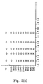
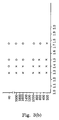
- the diagram shows the damage occurred (such as ripples or melting) as a function of the number of pulses given, and the level of energy fluence.
- the abscissa is the fluence given here as the ratio between the actual fluence (F) and the ablation threshold fluence and the ordinate is the number of pulses. Damage is indicated by o whereas a lack of damage (“no damage”) is indicated by x.
- Example 5 Same as Example 5, but the laser pulse was extended x3, as shown schematically in Fig. 4.
Landscapes
- Physics & Mathematics (AREA)
- Optics & Photonics (AREA)
- Engineering & Computer Science (AREA)
- Plasma & Fusion (AREA)
- Mechanical Engineering (AREA)
- General Physics & Mathematics (AREA)
- Drying Of Semiconductors (AREA)
- Laser Beam Processing (AREA)
- Cleaning Or Drying Semiconductors (AREA)
Claims (13)
- Ein Verfahren zum Verhindern der Oberflächen-Beschädigung eines Substrates beim Entfernen von Fotolacken von Substraten durch gepulste UV-Laser-Oberflächenbehandlung, unter Vorhandensein von reaktivem Gas, gekennzeichnet dadurch, dass es die Verlängerung der Laser-Impulse, bevor sie die Oberfläche erreichen, von der die Fotolacke entfernt werden sollen, umfasst.
- Ein Verfahren gemäß Anspruch 1, worin die Impuls-Dauer um das Zwei- bis Zwanzigfache verlängert wird.
- Ein Verfahren gemäß Anspruch 1, worin die Impuls-Verlängerung durch optische Mittel durchgeführt wird.
- Ein Verfahren gemäß Anspruch 1, das weiterhin die Homogenisierung des Impulses umfasst.
- Ein Verfahren gemäß Anspruch 4, worin die Homogenisierung durch optische Mittel erreicht wird.
- Ein Verfahren gemäß einem der Ansprüche 1 bis 5, worin das Substrat aus Halbleiter-Wafern und Flachbildschirmen gewählt wird.
- Ein Verfahren gemäß Anspruch 1, worin das Substrat ein Produkt auf einer Oberfläche ist, vom dem eine Schicht von Schutzmaterial aufgetragen wurde.
- Ein Verfahren gemäß Anspruch 7, worin das Substrat eine VLSI/ULSI-Schaltung ist.
- Vorrichtung zum Verhindern der Oberflächen-Beschädigung eines Substrats beim Entfernen von Fotolacken von Substraten (5), durch UV-Laser-Oberflächenbehandlung in einer Atmosphäre reaktiven Gases, die Mittel (1) zum Generieren eines gepulsten UV-Lasers und Mittel (4) zum Richten der Impulse auf die zu behandelnde Oberfläche umfasst, gekennzeichnet dadurch, dass sie weiter Folgendes umfasst:Mittel (2) zum Verlängern der Laser-Impulse, bevor sie die Oberfläche erreichen, von der die Fotolacke entfernt werden sollen; undwahlweise Mittel (3) zum Homogenisieren der Impulse.
- Vorrichtung gemäß Anspruch 9, worin die Mittel (3) zum Homogenisieren der Impulse nicht integral mit den Mitteln (2) zur Verlängerung der Impulse sind und worin sie extern und an die Vorrichtung gekoppelt sind.
- Vorrichtung zum Verhindern der Oberflächen-Beschädigung bei einem Objekt, das mit Laser behandelt wird, gemäß Anspruch 9 oder 10, wobei die Vorrichtung weiterhin Mittel zum Umlenken des Laserstrahls umfasst.
- Vorrichtung gemäß Anspruch 9, worin die Mittel zum Verlängern der Laser-Impulse optische Mittel sind.
- Vorrichtung gemäß einem der Ansprüche 9 bis 12, die Mittel zum Verlängern der Laser-Impuls-Dauer um das Zwei- bis Zwanzigfache umfasst.
Applications Claiming Priority (3)
| Application Number | Priority Date | Filing Date | Title |
|---|---|---|---|
| IL11593295 | 1995-11-09 | ||
| IL11593295A IL115932A0 (en) | 1995-11-09 | 1995-11-09 | Damage-free laser surface treatment method |
| PCT/IL1996/000139 WO1997017164A1 (en) | 1995-11-09 | 1996-11-04 | Damage-free laser surface treatment method |
Publications (2)
| Publication Number | Publication Date |
|---|---|
| EP0879113A1 EP0879113A1 (de) | 1998-11-25 |
| EP0879113B1 true EP0879113B1 (de) | 2004-05-26 |
Family
ID=11068162
Family Applications (1)
| Application Number | Title | Priority Date | Filing Date |
|---|---|---|---|
| EP96935312A Expired - Lifetime EP0879113B1 (de) | 1995-11-09 | 1996-11-04 | Schonendes laser-flächenbearbeitungsverfahren |
Country Status (7)
| Country | Link |
|---|---|
| EP (1) | EP0879113B1 (de) |
| JP (1) | JP2000500283A (de) |
| KR (1) | KR100483820B1 (de) |
| AU (1) | AU7331096A (de) |
| DE (1) | DE69632596T2 (de) |
| IL (1) | IL115932A0 (de) |
| WO (1) | WO1997017164A1 (de) |
Cited By (1)
| Publication number | Priority date | Publication date | Assignee | Title |
|---|---|---|---|---|
| DE102008041059A1 (de) * | 2008-08-06 | 2010-02-04 | Q-Cells Ag | Verfahren zur Herstellung einer strukturiert prozessierten oder strukturiert beschichteten Substratoberfläche |
Families Citing this family (5)
| Publication number | Priority date | Publication date | Assignee | Title |
|---|---|---|---|---|
| IL119246A (en) | 1996-09-12 | 2000-10-31 | Oramir Semiconductor Ltd | Laser removal of foreign materials from surfaces |
| US8066819B2 (en) | 1996-12-19 | 2011-11-29 | Best Label Co., Inc. | Method of removing organic materials from substrates |
| IL123416A0 (en) * | 1998-02-23 | 1998-09-24 | Oramir Semiconductor Ltd | Multi laser surface treatment in ambient fast flowing photoreactive gases |
| GB2347788A (en) * | 1999-03-06 | 2000-09-13 | Secr Defence | Forming devices such as ferroelectric infra-red sensors by annealing |
| US12074026B2 (en) * | 2022-05-19 | 2024-08-27 | Taiwan Semiconductor Manufacturing Co., Ltd. | Integrated photoresist removal and laser annealing |
Family Cites Families (2)
| Publication number | Priority date | Publication date | Assignee | Title |
|---|---|---|---|---|
| IL84255A (en) * | 1987-10-23 | 1993-02-21 | Galram Technology Ind Ltd | Process for removal of post- baked photoresist layer |
| US5312396A (en) * | 1990-09-06 | 1994-05-17 | Massachusetts Institute Of Technology | Pulsed laser system for the surgical removal of tissue |
-
1995
- 1995-11-09 IL IL11593295A patent/IL115932A0/xx unknown
-
1996
- 1996-11-04 KR KR10-1998-0703444A patent/KR100483820B1/ko not_active Expired - Fee Related
- 1996-11-04 JP JP9518031A patent/JP2000500283A/ja not_active Ceased
- 1996-11-04 EP EP96935312A patent/EP0879113B1/de not_active Expired - Lifetime
- 1996-11-04 AU AU73310/96A patent/AU7331096A/en not_active Abandoned
- 1996-11-04 WO PCT/IL1996/000139 patent/WO1997017164A1/en not_active Ceased
- 1996-11-04 DE DE69632596T patent/DE69632596T2/de not_active Expired - Fee Related
Cited By (1)
| Publication number | Priority date | Publication date | Assignee | Title |
|---|---|---|---|---|
| DE102008041059A1 (de) * | 2008-08-06 | 2010-02-04 | Q-Cells Ag | Verfahren zur Herstellung einer strukturiert prozessierten oder strukturiert beschichteten Substratoberfläche |
Also Published As
| Publication number | Publication date |
|---|---|
| DE69632596T2 (de) | 2005-06-23 |
| WO1997017164A1 (en) | 1997-05-15 |
| EP0879113A1 (de) | 1998-11-25 |
| DE69632596D1 (de) | 2004-07-01 |
| IL115932A0 (en) | 1996-01-31 |
| JP2000500283A (ja) | 2000-01-11 |
| KR100483820B1 (ko) | 2005-08-17 |
| KR19990067433A (ko) | 1999-08-16 |
| AU7331096A (en) | 1997-05-29 |
Similar Documents
| Publication | Publication Date | Title |
|---|---|---|
| US6350391B1 (en) | Laser stripping improvement by modified gas composition | |
| JP3410720B2 (ja) | 導電性溶液を用いた水晶基板のクリーニング方法 | |
| US20080299780A1 (en) | Method and apparatus for laser oxidation and reduction | |
| US5795831A (en) | Cold processes for cleaning and stripping photoresist from surfaces of semiconductor wafers | |
| US20040159335A1 (en) | Method and apparatus for removing organic layers | |
| US6933464B2 (en) | Laser-driven cleaning using reactive gases | |
| US20090258159A1 (en) | Novel treatment for mask surface chemical reduction | |
| US20080210269A1 (en) | Removing unwanted film from wafer edge region with reactive gas jet | |
| US6489590B2 (en) | Laser removal of foreign materials from surfaces | |
| EP0108189B1 (de) | Verfahren zum Ätzen von Polymiden | |
| KR100483820B1 (ko) | 표면손상을방지하기위한표면처리방법및장치 | |
| US6215099B1 (en) | Multi-Laser Combustion surface treatment | |
| US6123803A (en) | Laser processing chamber with cassette cell | |
| US6265138B1 (en) | Process and apparatus for oblique beam revolution, for the effective laser stripping of sidewalls | |
| IL124135A (en) | Damage-free laser surface treatment method | |
| US20110061679A1 (en) | Photoreactive Removal of Ion Implanted Resist | |
| JP2004157424A (ja) | レジストの剥離方法及び半導体装置の製造方法 | |
| JP3329200B2 (ja) | 半導体装置の製造方法および装置 | |
| KR100780290B1 (ko) | 포토레지스트 제거 공정구현 설비 | |
| EP0710161A1 (de) | Nachbehandlung eines beschichteten substrates mit einem angeregtes halogen enthaltenden gas für die beseitigung von rückständen | |
| WO2007019287A2 (en) | Photoreactive removal of ion implanted resist | |
| Lee et al. | Optoelectrical and optoacoustic analysis of the laser cleaning process of a photoresist on Si and ITO | |
| IL124136A (en) | Process and apparatus for oblique beam revolution, for the effective laser stripping of sidewalls |
Legal Events
| Date | Code | Title | Description |
|---|---|---|---|
| PUAI | Public reference made under article 153(3) epc to a published international application that has entered the european phase |
Free format text: ORIGINAL CODE: 0009012 |
|
| 17P | Request for examination filed |
Effective date: 19980602 |
|
| AK | Designated contracting states |
Kind code of ref document: A1 Designated state(s): BE CH DE FR GB IE IT LI NL SE |
|
| 17Q | First examination report despatched |
Effective date: 20000620 |
|
| GRAP | Despatch of communication of intention to grant a patent |
Free format text: ORIGINAL CODE: EPIDOSNIGR1 |
|
| GRAS | Grant fee paid |
Free format text: ORIGINAL CODE: EPIDOSNIGR3 |
|
| GRAA | (expected) grant |
Free format text: ORIGINAL CODE: 0009210 |
|
| AK | Designated contracting states |
Kind code of ref document: B1 Designated state(s): BE CH DE FR GB IE IT LI NL SE |
|
| PG25 | Lapsed in a contracting state [announced via postgrant information from national office to epo] |
Ref country code: NL Free format text: LAPSE BECAUSE OF FAILURE TO SUBMIT A TRANSLATION OF THE DESCRIPTION OR TO PAY THE FEE WITHIN THE PRESCRIBED TIME-LIMIT Effective date: 20040526 Ref country code: LI Free format text: LAPSE BECAUSE OF FAILURE TO SUBMIT A TRANSLATION OF THE DESCRIPTION OR TO PAY THE FEE WITHIN THE PRESCRIBED TIME-LIMIT Effective date: 20040526 Ref country code: IT Free format text: LAPSE BECAUSE OF FAILURE TO SUBMIT A TRANSLATION OF THE DESCRIPTION OR TO PAY THE FEE WITHIN THE PRESCRIBED TIME-LIMIT;WARNING: LAPSES OF ITALIAN PATENTS WITH EFFECTIVE DATE BEFORE 2007 MAY HAVE OCCURRED AT ANY TIME BEFORE 2007. THE CORRECT EFFECTIVE DATE MAY BE DIFFERENT FROM THE ONE RECORDED. Effective date: 20040526 Ref country code: CH Free format text: LAPSE BECAUSE OF FAILURE TO SUBMIT A TRANSLATION OF THE DESCRIPTION OR TO PAY THE FEE WITHIN THE PRESCRIBED TIME-LIMIT Effective date: 20040526 Ref country code: BE Free format text: LAPSE BECAUSE OF FAILURE TO SUBMIT A TRANSLATION OF THE DESCRIPTION OR TO PAY THE FEE WITHIN THE PRESCRIBED TIME-LIMIT Effective date: 20040526 |
|
| REG | Reference to a national code |
Ref country code: GB Ref legal event code: FG4D |
|
| REG | Reference to a national code |
Ref country code: CH Ref legal event code: EP |
|
| REG | Reference to a national code |
Ref country code: IE Ref legal event code: FG4D |
|
| REF | Corresponds to: |
Ref document number: 69632596 Country of ref document: DE Date of ref document: 20040701 Kind code of ref document: P |
|
| PG25 | Lapsed in a contracting state [announced via postgrant information from national office to epo] |
Ref country code: SE Free format text: LAPSE BECAUSE OF FAILURE TO SUBMIT A TRANSLATION OF THE DESCRIPTION OR TO PAY THE FEE WITHIN THE PRESCRIBED TIME-LIMIT Effective date: 20040826 |
|
| PG25 | Lapsed in a contracting state [announced via postgrant information from national office to epo] |
Ref country code: IE Free format text: LAPSE BECAUSE OF NON-PAYMENT OF DUE FEES Effective date: 20041104 Ref country code: GB Free format text: LAPSE BECAUSE OF NON-PAYMENT OF DUE FEES Effective date: 20041104 |
|
| REG | Reference to a national code |
Ref country code: CH Ref legal event code: PL |
|
| NLV1 | Nl: lapsed or annulled due to failure to fulfill the requirements of art. 29p and 29m of the patents act | ||
| ET | Fr: translation filed | ||
| PLBE | No opposition filed within time limit |
Free format text: ORIGINAL CODE: 0009261 |
|
| STAA | Information on the status of an ep patent application or granted ep patent |
Free format text: STATUS: NO OPPOSITION FILED WITHIN TIME LIMIT |
|
| 26N | No opposition filed |
Effective date: 20050301 |
|
| PG25 | Lapsed in a contracting state [announced via postgrant information from national office to epo] |
Ref country code: DE Free format text: LAPSE BECAUSE OF NON-PAYMENT OF DUE FEES Effective date: 20050601 |
|
| GBPC | Gb: european patent ceased through non-payment of renewal fee |
Effective date: 20041104 |
|
| REG | Reference to a national code |
Ref country code: IE Ref legal event code: MM4A |
|
| PGFP | Annual fee paid to national office [announced via postgrant information from national office to epo] |
Ref country code: FR Payment date: 20071130 Year of fee payment: 12 |
|
| REG | Reference to a national code |
Ref country code: FR Ref legal event code: ST Effective date: 20110331 |
|
| PG25 | Lapsed in a contracting state [announced via postgrant information from national office to epo] |
Ref country code: FR Free format text: LAPSE BECAUSE OF NON-PAYMENT OF DUE FEES Effective date: 20041130 |