EP0879902A2 - Treating method and apparatus utilizing chemical reaction - Google Patents
Treating method and apparatus utilizing chemical reaction Download PDFInfo
- Publication number
- EP0879902A2 EP0879902A2 EP98303765A EP98303765A EP0879902A2 EP 0879902 A2 EP0879902 A2 EP 0879902A2 EP 98303765 A EP98303765 A EP 98303765A EP 98303765 A EP98303765 A EP 98303765A EP 0879902 A2 EP0879902 A2 EP 0879902A2
- Authority
- EP
- European Patent Office
- Prior art keywords
- reaction
- chemical reaction
- solution
- reaction solution
- gas
- Prior art date
- Legal status (The legal status is an assumption and is not a legal conclusion. Google has not performed a legal analysis and makes no representation as to the accuracy of the status listed.)
- Granted
Links
Images


Classifications
-
- H—ELECTRICITY
- H10—SEMICONDUCTOR DEVICES; ELECTRIC SOLID-STATE DEVICES NOT OTHERWISE PROVIDED FOR
- H10P—GENERIC PROCESSES OR APPARATUS FOR THE MANUFACTURE OR TREATMENT OF DEVICES COVERED BY CLASS H10
- H10P50/00—Etching of wafers, substrates or parts of devices
- H10P50/60—Wet etching
- H10P50/61—Electrolytic etching
- H10P50/613—Electrolytic etching of Group IV materials
-
- C—CHEMISTRY; METALLURGY
- C25—ELECTROLYTIC OR ELECTROPHORETIC PROCESSES; APPARATUS THEREFOR
- C25D—PROCESSES FOR THE ELECTROLYTIC OR ELECTROPHORETIC PRODUCTION OF COATINGS; ELECTROFORMING; APPARATUS THEREFOR
- C25D11/00—Electrolytic coating by surface reaction, i.e. forming conversion layers
- C25D11/005—Apparatus specially adapted for electrolytic conversion coating
-
- C—CHEMISTRY; METALLURGY
- C25—ELECTROLYTIC OR ELECTROPHORETIC PROCESSES; APPARATUS THEREFOR
- C25D—PROCESSES FOR THE ELECTROLYTIC OR ELECTROPHORETIC PRODUCTION OF COATINGS; ELECTROFORMING; APPARATUS THEREFOR
- C25D11/00—Electrolytic coating by surface reaction, i.e. forming conversion layers
- C25D11/02—Anodisation
- C25D11/32—Anodisation of semiconducting materials
-
- H—ELECTRICITY
- H10—SEMICONDUCTOR DEVICES; ELECTRIC SOLID-STATE DEVICES NOT OTHERWISE PROVIDED FOR
- H10P—GENERIC PROCESSES OR APPARATUS FOR THE MANUFACTURE OR TREATMENT OF DEVICES COVERED BY CLASS H10
- H10P90/00—Preparation of wafers not covered by a single main group of this subclass, e.g. wafer reinforcement
- H10P90/19—Preparing inhomogeneous wafers
- H10P90/1904—Preparing vertically inhomogeneous wafers
- H10P90/1906—Preparing SOI wafers
- H10P90/1922—Preparing SOI wafers using silicon etch back techniques, e.g. BESOI or ELTRAN
-
- H—ELECTRICITY
- H10—SEMICONDUCTOR DEVICES; ELECTRIC SOLID-STATE DEVICES NOT OTHERWISE PROVIDED FOR
- H10W—GENERIC PACKAGES, INTERCONNECTIONS, CONNECTORS OR OTHER CONSTRUCTIONAL DETAILS OF DEVICES COVERED BY CLASS H10
- H10W10/00—Isolation regions in semiconductor bodies between components of integrated devices
- H10W10/10—Isolation regions comprising dielectric materials
- H10W10/181—Semiconductor-on-insulator [SOI] isolation regions, e.g. buried oxide regions of SOI wafers
Definitions
- the present invention relates to a treating method and apparatus utilizing a chemical reaction and, more particularly to a treating method and apparatus utilizing a chemical reaction, applicable to production of chemical industrial goods and semiconductor goods such as integrated circuits or electron devices.
- Treating methods utilizing chemical reactions have been and are applied to many chemical industrial goods and also to semiconductor integrated circuits these years, thus adding abundance to human lives.
- electrolysis reaction is the technology for supplying electric energy to an electrolytic cell to cause change in substance at the interface between the electrode and the electrolyte, thereby producing a chemical substance as an objective material.
- This technology is applied to production of many industrial goods, including smelting of aluminum, copper, or zinc, metal plating, production of hydrogen, oxygen, caustic soda, and chlorine, and so on.
- These utilize the chemical reaction in a solution, called anodization, and are methods for producing a semiconductor substrate characterized by epitaxially growing single-crystal silicon on one porous surface of a silicon single-crystal substrate having made porous a part or all of the surface side by the anodization process, bonding a surface of this epitaxial layer to an arbitrary support substrate, and selectively etching the porous portion of the single-crystal silicon substrate, or removing the non-porous portion by polishing and then selectively etching the porous portion, or separating the bonded substrate into the non-porous portion and an SOI substrate at the porous portion.
- porous silicon formed by the anodization reaction has an enormous surface area and the surface thereof is active to adsorption of an organic gas
- gas sensors utilizing the property are under research (M. B-Chohrin and A. Kurex, "Absorbate effects on photoluminescence and electrical conductivity of porous silicon,” Appl. Phys. Lett., vol. 64, pp. 481-483, 1994; A. Richter, “Design considerations and performance of adsorptive humidity sensor with capacitive readout," The 7th Int. Conf. Solid-State Sensors and Actuators, pp. 310-313, 1993; R. C. Anderson, R. S. Muller, and C. W.
- the chemical reactions in a solution are widely used in production of industrial goods, for example, in the chemical industries and the semiconductor industries.
- increasing the efficiency of chemical reaction is very important in order to raise economical efficiency of material production or resource savings.
- the semiconductor industries from the viewpoint of pursuit of cost efficiency, there are two more requirements of increase in rates of such a chemical reaction as film formation or etching and in-plane uniformity of chemical reactions on a large-diameter silicon wafer.
- the chemical reaction in a solution involves generation of a reaction by-product, which is a phenomenon of inhibiting increase in efficiency, rate, and uniformity of chemical reactions. That is, presence in the solution of a further reaction by-product formed by the chemical reaction in addition to the objective chemical substance will inhibit progress of the chemical reaction.
- a typical example is a phenomenon in the electrolysis in an aqueous solution where hydrogen is normally generated at the negative electrode while oxygen is generated at the positive electrode.
- the process includes a treatment such as adding alcohol as a surfactant or agitating the solution by use of an agitator.
- a treatment such as adding alcohol as a surfactant or agitating the solution by use of an agitator.
- These treating methods are temporary solutions, but are not essential solutions.
- pores having diameters of about 10 nm and depths of about 20 ⁇ m need to be formed with restraining fluctuation within ⁇ 5% as to the diameters of pores and within ⁇ 10% as to the depths of pores in the silicon wafer plane.
- this process of formation of a porous silicon layer has to be carried out in one minute, which is a standard process time in recent volume production of semiconductors.
- the reaction solution has to be always supplied to the bottoms of the fine and long pores having the aspect ratio of 2000 while perfectly removing this large amount of hydrogen as the by-product.
- An object of the present invention is to provide a method and apparatus wherein a chemical reaction is carried out while the concentration of a gas of a reaction by-product dissolved in a reaction solution in a reaction vessel is always maintained to be not more than its solubility during the reaction.
- the chemical reaction in a solution may be an electrochemical reaction with supply of an electrical energy from outside and, of course, may be an anodization reaction as a kind of electrochemical reactions.
- the solution may be an electrolyte.
- the reaction solution in order to always maintain the concentration of a gas of a reaction by-product dissolved in the reaction solution in the reaction vessel to be not more than the solubility during the reaction, the reaction solution is circulated outside the reaction vessel, for example, and it is deaerated on the way of circulation, preferably.
- the concentration of a gas of a reaction by-product be controlled so as to be not more than 1/10 of the solubility.
- concentration of gas is controlled to be not more than 1/10 of the solubility, for example, in the case of a reaction for forming a porous layer in a surface of a substrate by an anodization reaction where the substrate is held in the reaction vessel, at least one surface of the substrate is kept in contact with the reaction solution, the other surface of the substrate is kept in contact with an electrically conductive solution, a negative voltage is applied to the reaction solution, and a positive voltage is applied to the conductive solution, the porous layer with deep pores having the diameter of 10 nm and the depth of 20 ⁇ m, thus having the aspect ratio of pore of 2000, can be formed in a treatment time of one minute while restraining the variation in the depths of pores within ⁇ 3% in a plane of a 6-inch wafer, by maintaining the amount of dissolved hydrogen in the reaction solution at 1/10 of
- the concentration of gas is particularly preferably controlled so as to be not more than 100 ppb.
- concentration of gas is controlled to be not more than 100 ppb, for example, in the reaction for forming the porous layer in the surface of substrate by the anodization reaction where the substrate is held in the reaction vessel, one surface of the substrate is kept in contact with the reaction solution, the other surface of the substrate is kept in contact with the electrically conductive solution, the negative voltage is applied to the reaction solution, and the positive voltage is applied to the conductive solution, the porous layer with deep pores having the diameter of 10 nm and the depth of 20 ⁇ m, thus having the aspect ratio of pore of 2000, can be formed in the treatment time of one minute while restraining the variation in the depths of pores within ⁇ 3% in the 6-inch wafer plane.
- the same gas as the reaction by-product exists in the reaction solution from the beginning.
- Such the gas should desirably be removed before the reaction.
- the gas having particularly great effects is the by-product generated in the chemical reaction.
- This by-product generated in the chemical reaction needs to be removed at the same time as the generation thereof, so that no bubble of the by-product is generated.
- it is particularly effective to guide the reaction solution to the outside of the reaction system and to perform deaeration outside the system. Accordingly, the deaeration is preferably carried out in a circulation system.
- Chemical reactions accompanied by generation of by-products are, for example, electrochemical reactions, anodization reactions, and so on, and the present invention is particularly effective in these chemical reactions.
- the reaction of forming the porous layer in the surface of the substrate by the anodization reaction where the substrate is held in the reaction vessel, at least one surface of the substrate is kept in contact with the reaction solution with the other surface of the substrate in contact with the conductive solution, the negative voltage is applied to the reaction solution with the positive voltage applied to the conductive solution, the by-product (gas) will remain in the pores.
- this tendency is particularly conspicuous where the diameters of the pores are 20 nm or less, where the depths of pores are 20 ⁇ m or more, and where the aspect ratios of the pores are 1000 or more. As a result, nonuniformity occurs in formation of the pores. This tendency is further enhanced in the case of treatments in a shorter time.
- the diameters of the pores are 10 nm, the depths of the pores are 20 ⁇ m, and the aspect ratios of the pores are 2000, formation of uniform pores can be realized even in the case of the treatment time of one minute.
- the reaction solution is preferably isolated from the atmosphere. This is for preventing a gas from mixing from the atmosphere into the reaction solution.
- the deaeration may be carried out with a deaerating module comprised of a gas-permeable membrane of hollow fibers, either by evacuating the inside of the hollow fibers to a reduced pressure state by means of a vacuum pump or by filling the inside of the hollow fibers with ultrapure water containing no gas molecule at all.
- control within the fluctuation of ⁇ 0.5°C is preferable in terms of enhancement of controllability of the chemical reaction.
- Another object of the present invention is to provide a chemical reaction apparatus comprising:
- An example of the chemical reaction apparatus is an apparatus for carrying out the anodization treatment.
- one surface of a substrate is kept in contact with a reaction solution
- the other surface of the substrate is kept in contact with an electrically conductive solution
- the concentration of gas molecules dissolved in the solution is always controlled so as to be not more than the solubility, for example, in the pore formation reaction of silicon by anodization, the gas molecules of the by-product are prevented from forming bubbles and then adhering onto silicon, more particularly onto the bottoms of the pores of silicon, which in turn enables to suppress degradation of chemical reaction rate and occurrence of nonuniform chemical reaction.
- the present invention it is possible to perform pore formation in the silicon substrate for use in the field of ordinary semiconductor integrated circuits, with in-plane uniformity and at high speed. Further, according to the present invention, a semiconductor substrate applicable to formation of SOI structure can be produced. In addition, according to the present invention, it is possible to produce a semiconductor substrate in which a light-emitting element or a gas sensor can be formed, on the basis of an inexpensive silicon substrate.
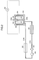
- Fig. 1 and Fig. 2 are schematic views showing a chemical reaction apparatus according to a preferred embodiment of the present invention.
- the chemical reaction apparatus has a reaction vessel 300 having a holding means 206a, 206b for holding a substrate (for example, a silicon wafer or a substrate with a silicon layer) 200, for housing a reaction solution (for example, a liquid containing hydrofluoric acid) 201 and for performing a chemical reaction with the substrate 200 therein; a circulation line 210a (outward path), 210b (inward path) for circulating the reaction solution 201 outside the reaction vessel 300; a deaerating device 301 provided on the circulation line 210a, for removing a gas from the reaction solution 201; and a transfer pump 303 which is a transfer means for transferring the reaction solution 201 on the circulation line 210a.
- the concentration of the gas dissolved in the reaction solution is always maintained at or below the solubility thereof by use of the deaerating device.
- This example is the chemical reaction apparatus for anodization, in which one surface of the substrate 200 is in contact with the reaction solution (for example, a liquid containing hydrofluoric acid) 201 and in which the other surface of the substrate 200 is in contact with an electrolyte 202, which is an electrically conductive solution, and the apparatus is provided with a negative electrode 203 for applying a negative voltage to the reaction solution 201 and a positive electrode 204 for applying a positive voltage to the conductive solution 202.
- the reaction solution for example, a liquid containing hydrofluoric acid
- the substrate 200 is held vertically by the holding means 206a, 206b and this substrate 200 itself separates the reaction solution 201 and the electrolyte 202.
- sealing with seal 205 for example, of Goatex is provided between the holding means and the substrate 200.
- a cooler and/or a heater, or a heat exchanger 302 is provided on the circulation line 210b as occasion may demand, and the reaction solution under circulation is heated or cooled thereby.
- This heating/cooling is preferably carried out so that the temperature of the reaction solution 201 in the reaction vessel 300 is kept within the variation of ⁇ 0.5°C.
- the apparatus is provided with a sensor (not shown) for detecting the temperature of the reaction solution 201 in the reaction vessel 300 and is so arranged as to adjust heating/cooling amounts by the cooler and/or heater, or heat exchanger 302, based on a signal from the sensor.
- Numeral 304 designates a filter, which removes particles of 0.1 ⁇ m or more.
- the deaerating device 301 used in the present invention will be described below.
- the deaerating device 301 is composed of a deaerating module 401 and a vacuum pump 400; in the example shown in Fig. 4, the deaerating device 301 is composed of a deaerating module 401 and a water generator 500.
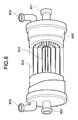
- FIG. 8 A structural example of the deaerating module is shown in Fig. 8.
- the deaerating module 401 has the structure in which hollow-fiber separation membrane sheet 804 woven like a bamboo blind is wound in a spiral form around a perforated water supply pipe 803 having many holes and located in the center, for example, as shown in Fig. 8.
- a perforated water supply pipe 803 having many holes and located in the center, for example, as shown in Fig. 8.
- the hollow fiber separation membrane sheet 804 is made of, for example, a fluororesin such as PFA, and therefore does not suffer deterioration at all even if the reaction solution 200 is a hydrofluoric-acid-based reaction solution, i.e., a liquid containing hydrofluoric acid.
- the inside of the hollow fibers is kept in a pressure reduced state by evacuating the inside by the vacuum pump 400 through hollow fiber ports 802.
- the gas dissolved in the reaction solution 200 efficiently moves from the outside to the inside of the hollow fibers while the reaction solution 200 passes through the laminated portion of the bamboo blind like member of the hollow fibers, and is discharged to the outside of the system through the vacuum pump 400.
- the deaerating device 301 is of the structure of Fig. 4, ultrapure water containing no gas molecule at all, generated by the water generator 500, is forced to the hollow fiber port 802 to be discharged from the other hollow fiber port, whereby a state is kept in which the inside of the hollow fibers is filled with the ultrapure water containing no gas molecule at all.
- the gas molecules in the solution efficiently move from the outside to the inside of the hollow fibers during the period of passage through the laminated portion of the bamboo blind like member of the hollow fibers and are discharged to the outside of the system.
- anodization As the treatments utilizing chemical reactions in the present invention, there may be included such treatments as anodization, anodic oxidation, electrolytic etching, or the like. Among such treatments, examples of anodization will be described.
- the substrate is a substrate 200 comprising p-type single-crystal silicon. It is not impossible to employ the n-type, but a low-resistance substrate has to be selected in that case.
- the substrate 200 is set in the reaction vessel 300 as shown in Fig. 1.
- the reaction vessel 300 is of a completely closed type in order to avoid contact of the solution 201 or electrolyte 202 with the external air. Namely, one side of the substrate 200 is in contact with the hydrofluoric-acid-based reaction solution 201 and the negative electrode 203 is placed on the side of the reaction solution 201.
- the other side of the substrate 200 is in contact with the electrolyte 202 and the positive electrode 204 is placed on the side of the electrolyte 202.
- the electrolyte 202 may be any electrically conductive solution and thus may be the hydrofluoric-acid-based reaction solution. In either case the pore forming reaction takes place from the negative electrode side of the substrate 200 in contact with the hydrofluoric-acid-based solution.
- As the hydrofluoric-acid-based reaction solution 201 concentrated hydrofluoric acid (49 wt% HF) is normally used.
- a surfactant needs to be added into the electrolyte as the reaction solution.
- an alcohol is desired which has the action of lowering the surface tension of the reaction solution 201 and poses no problem of adherence of the surfactant to the substrate 200 in a cleaning step after the anodization.
- an alcohol there may be used, for example, methanol, ethanol, propanol, IPA (isopropyl alcohol), and so on. Since the above example is of the anodization of Si, the reaction solution is the liquid containing hydrofluoric acid; however, it is a matter of course that the reaction solution can be any other non-hydrofluoric-acid-based electrolyte.
- the negative electrode 203 or the positive electrode 204 there my be used a material that is not corroded by the hydrofluoric acid solution, for example, gold (Au), platinum (Pt), or the like.
- the reaction solution 201 in the reaction vessel 300 is circulated through the deaerating device 301 and the cooler/heater 302 as shown in Fig. 2.
- the deaerating device 301 has the structure in which deaerating modules 401 using a gas-permeable membrane are connected in parallel.
- the gas-permeable membrane there exist porous and non-porous ones. Since the circulated solution is the reaction solution containing alcohol serving as a surfactant, the gas-permeable membrane is desirably selected from the non-porous membranes, taking exudation of the reaction solution through the gas-permeable membrane into consideration.
- the deaerating modules 401 have the structure in which the hollow fiber separation membrane sheet woven like the bamboo blind is wound in the spiral form around the perforated supply pipe at the center, and the inside of the hollow fibers is kept in the pressure reduced state by the vacuum pump 400 as shown in Fig. 3.
- the inside of the hollow fibers is kept in the pressure reduced state by the vacuum pump 400, and the gas molecules in the solution efficiently move from the outside to the inside of the hollow fibers during the period of passage through the laminated portions of the hollow fiber bamboo blind like member because of the pressure difference between the inside and outside of the hollow fibers constituted of the gas-permeable membrane, to be discharged through the vacuum pump 400 to the outside of the system.
- the cooler/heater 302 capable of cooling or heating the solution controls the fluctuation of temperature of the reaction solution 201 in the reaction vessel 300 within ⁇ 0.5°C.
- the above arrangement makes it possible to always control the concentration of gas molecules dissolved in the solution at or below the solubility in the chemical reaction in the solution, the gas molecules of by-product are prevented from forming bubbles in the pore forming reaction of silicon and from in turn adhering onto silicon, more specifically to the bottoms of the pores of the silicon, whereby it becomes possible to suppress degradation of chemical reaction rate and nonuniformity of chemical reaction.
- a method for forming porous silicon or a porous silicon substrate by anodizing a single-crystal silicon substrate As the substrate, is provided a substrate 200 comprising p-type single-crystal silicon. It is not impossible to employ the n-type, but a low-resistance substrate has to be selected in that case.
- the substrate 200 is set in the reaction vessel 300 as shown in Fig. 1.
- the reaction vessel 300 is of the completely closed type in order to avoid contact of the solution 201 or electrolyte 202 with the external air. Namely, one side of the substrate 200 is in contact with the hydrofluoric-acid-based reaction solution 201 and the negative electrode 203 is placed on the side of the reaction solution 201. On the other hand, the other side of the substrate 200 is in contact with the electrolyte 202 and the positive electrode 204 is placed on the side of the electrolyte 202.
- the electrolyte 202 may be any electrically conductive solution and thus may be the hydrofluoric-acid-based reaction solution.
- the pore forming reaction occurs from the negative electrode side of the substrate 200 in contact with the hydrofluoric-acid-based solution.
- hydrofluoric-acid-based reaction solution 201 concentrated hydrofluoric acid (49 wt% HF) is normally used.
- the surfactant an alcohol which has the action of lowering the surface tension of the reaction solution 201 and poses no problem of adherence of the surfactant to the substrate 200 in the cleaning step after the anodization.
- the alcohol there may be used, for example, methanol, ethanol, propanol, IPA, and so on.
- the negative electrode 203 or the positive electrode 204 there may be used a material that is not corroded by the hydrofluoric acid solution, for example, gold (Au), platinum (Pt), or the like.
- the reaction solution 201 in the reaction vessel 300 is circulated through the deaerating device 301 and the cooler/heater 302 as shown in Fig. 2.
- the deaerating device 301 has the structure in which deaerating modules 401 using the gas-permeable membrane are connected in parallel.
- As the gas-permeable membrane there exist porous and non-porous ones. Since the circulated solution is the reaction solution containing alcohol serving as a surfactant, the gas-permeable membrane is desirably selected from the non-porous membranes, taking exudation of the reaction solution through the gas-permeable membrane into consideration.
- the deaerating modules 401 have the structure in which the hollow fiber separation membrane sheet woven like the bamboo blind is wound in the spiral form around the perforated supply pipe at the center, and the inside of the hollow fibers is kept in the state filled with the ultrapure water containing no gas molecule at all from the water generator 500 as shown in Fig. 4.
- the inside of the hollow fibers is kept in the state filled with the ultrapure water containing no gas molecule at all, and the gas molecules in the solution efficiently move from the outside to the inside of the hollow fibers during the period of passage through the laminated portions of the hollow fiber bamboo blind like member because of the difference between the internal and external partial pressures of the gas component with respect to the hollow fibers constituted of the gas-permeable membrane, to be discharged to the outside of the system.
- the cooler/heater 302 controls the fluctuation of temperature of the reaction solution 201 in the reaction vessel 300 within ⁇ 0.5°C.
- the above arrangement makes it possible to always control the concentration of gas molecules dissolved in the solution at or below the solubility in the chemical reaction in the solution, the gas molecules of by-product are prevented from forming bubbles in the pore forming reaction of a silicon wafer and from in turn adhering onto the silicon wafer, more specifically, to the bottoms of the pores of the silicon wafer, whereby it becomes possible to suppress degradation of chemical reaction rate and nonuniformity of chemical reaction.
- First prepared was the (100) single-crystal silicon substrate 200 of 6-inch p + -substrate having the thickness of 625 ⁇ m, at least the surface layer of which was doped with boron in 1 to 10 ⁇ 10 18 cm -3 , and the surface thereof was subjected to the anodization treatment using a p + -layer of Si as an opposed electrode in a solution of HF/H 2 O/IPA (20 to 30 wt% HF, 10 to 30 wt% IPA). The current density at that time was 5 mA/cm 2 .
- the reaction solution 201 in the reaction vessel 300 was circulated through the deaerating device 301 and the cooler/heater 302.
- the deaerating device 301 was composed of seven deaerating modules 401 formed by use of the non-porous gas-permeable membrane, connected in parallel.
- the deaerating device 301 was kept in the pressure reduced state of about 10 Torr, using the vacuum pump 400.
- the transfer pump 303 was the one capable of circulating the reaction solution at the flow rate of 70 l/min through the chemical circulation line, i.e., capable of circulating the reaction solution at the flow rate per deaerating module of 10 l/min.
- Amounts of dissolved hydrogen in the reaction solution 201 in the reaction vessel 300 were observed on that occasion, and the result was that during the anodization treatment the amounts of dissolved hydrogen were always approximately 100 ppb or less, far smaller than 1 ppm being the solubility thereof.
- the variation of temperature of the reaction solution 201 in the reaction vessel 300 was always controlled within ⁇ 0.5°C by actuating the cooler/heater 302.
- the anodization treatment was carried out for one minute and the entire surface of the 6-inch wafer was observed with a field emission type scanning electron microscope. It was found from the observation that a layer of porous Si having the diameter of pore of 10 nm, the aperture rate of 30%, and the film thickness of 20 ⁇ m was formed with the in-plane uniformity being within the fluctuation of ⁇ 3%. Cross sections of the porous layer were also observed with a transmission electron microscope, with the result that it was confirmed that new crystal defects were not introduced into the porous layer and good single crystallinity was maintained.
- First prepared was the (100) single-crystal silicon substrate 200 of 6-inch p + -substrate having the thickness of 625 ⁇ m, at least the surface layer of which was doped with boron in 1 to 10 ⁇ 10 18 cm -3 , and the surface thereof was subjected to the anodization treatment using the p + -layer of Si as an opposed electrode in the solution of HF/H 2 O/IPA (20 to 30 wt% HF, 10 to 30 wt% IPA). The current density at that time was 5 mA/cm 2 .
- the reaction solution 201 in the reaction vessel 300 was circulated through the deaerating device 301 and the cooler/heater 302.
- the deaerating device 301 was composed of seven deaerating modules 401 formed by use of the non-porous gas-permeable membrane, connected in parallel. The deaerating device 301 was kept in the state filled with the ultrapure water containing no gas molecule at all, supplied from the water generator 500.
- the transfer pump 303 was the one capable of circulating the reaction solution at the flow rate of 70 l/min through the chemical circulation line, i.e., capable of circulating the reaction solution at the flow rate per deaerating module of 10 l/min. Amounts of dissolved hydrogen in the reaction solution 201 in the reaction vessel 300 were observed on that occasion, and the result was that during the anodization treatment the amounts of dissolved hydrogen were always approximately 100 ppb or less, far smaller than 1 ppm being the solubility thereof. During the anodization treatment the variation of temperature of the reaction solution 201 in the reaction vessel 300 was always controlled within ⁇ 0.5°C by actuating the cooler/heater 302.
- the anodization treatment was carried out for one minute and the entire surface of the 6-inch wafer was observed with the field emission type scanning electron microscope. It was found from the observation that a layer of porous Si having the diameter of pore of 10 nm, the aperture rate of 30%, and the film thickness of 20 ⁇ m was formed with the in-plane uniformity being within the fluctuation of ⁇ 3%.
- First prepared was the (100) single-crystal silicon substrate 200 of 6-inch p + -substrate having the thickness of 625 ⁇ m, at least the surface layer of which was doped with boron in 1 to 10 ⁇ 10 18 cm -3 , and the surface thereof was subjected to the anodization treatment using the p + -layer of Si as an opposed electrode in the solution of HF/H 2 O/IPA (20 to 30 wt% HF, 10 to 30 wt% IPA). The current density at that time was 5 mA/cm 2 .
- the reaction solution 201 in the reaction vessel 300 was circulated through the deaerating device 301 and the cooler/heater 302.
- the deaerating device 301 was composed of seven deaerating modules 401 formed by use of the non-porous gas-permeable membrane, connected in parallel.
- the deaerating device 301 was kept in the state filled with the ultrapure water containing no gas molecule at all, supplied from the water generator 500.
- the temperature variation of the reaction solution 201 in the reaction vessel 300 was always controlled within ⁇ 0.5 °C by actuating the cooler/heater 302.
- Fig. 5 shows the dispersion in the depths of pores of the wafer in the respective amounts of dissolved hydrogen. As the amounts of dissolved hydrogen increase, the depths of pores become smaller and the dispersion in the depths of pores increases.
- the porous layer having the diameter of pore of 10 nm and the aperture rate of 30% was formed in the film thickness of 20 ⁇ m and with the in-plane uniformity of film thickness being within the dispersion of ⁇ 3% in the treatment time of one minute.
- First prepared was the (100) single-crystal silicon substrate 200 of 6-inch p + -substrate having the thickness of 625 ⁇ m, at least the surface layer of which was doped with boron in 1 to 10 ⁇ 10 18 cm -3 , and the surface thereof was subjected to the anodization treatment using the p + -layer of Si as an opposed electrode in the solution of HF/H 2 O/IPA (20 to 30 wt% HF, 10 to 30 wt% IPA). As shown in Fig. 2, the reaction solution 201 in the reaction vessel 300 was circulated through the deaerating device 301 and the cooler/heater 302.
- the deaerating device 301 was composed of seven deaerating modules 401 formed by use of the non-porous gas-permeable membrane, connected in parallel. The deaerating device 301 was kept in the state filled with the ultrapure water containing no gas molecule at all, supplied from the water generator 500.
- the transfer pump 303 was the one capable of circulating the reaction solution at the flow rate of 35 l/min through the chemical circulation line, i.e., capable of circulating the reaction solution at the flow rate per deaerating module of 5 l/min. Amounts of dissolved hydrogen in the reaction solution 201 in the reaction vessel 300 were observed on that occasion, and the result was that during the anodization treatment the amounts of dissolved hydrogen were always approximately 600 ppb during the anodization treatment. During the anodization treatment the variation of temperature of the reaction solution 201 in the reaction vessel 300 was always controlled within ⁇ 0.5 °C by actuating the cooler/heater 302.
- the anodization treatment was carried out under conditions of different current densities ranging from 5 to 30 mA/cm 2 , and the entire surface of the 6-inch wafer was observed thereafter with the field emission type scanning electron microscope.
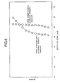
- Fig. 6 shows the dispersion in the depths of pores of the wafer in the respective current densities.
- the diameters of the pores increase with increase in the current density. It was found that when the amount of dissolved hydrogen in the reaction solution 201 in the reaction vessel 300 was 600 ppb, the fluctuation of in-plane uniformity of film thickness was restrained within ⁇ 3% in formation of the porous layer having the diameter of pore of 20 nm and the depth of pore of 20 ⁇ m, i.e., having the aspect ratio of pore of 1000.
- First prepared was the (100) single-crystal silicon substrate 200 of 6-inch p + -substrate having the thickness of 625 ⁇ m, at least the surface layer of which was doped with boron in 1 to 10 ⁇ 10 18 cm -3 , and the surface thereof was subjected to the anodization treatment using the p + -layer of Si as an opposed electrode in the solution of HF/H 2 O/IPA (20 to 30 wt% HF, 10 to 30 wt% IPA). The current density at that time was 5 mA/cm 2 .
- the reaction solution 201 in the reaction vessel 300 was circulated through the deaerating device 301 and the cooler/heater 302.
- the deaerating device 301 was composed of seven deaerating modules 401 formed by use of the non-porous gas-permeable membrane, connected in parallel.
- the deaerating device 301 was kept in the state filled with the ultrapure water containing no gas molecule at all, supplied from the water generator 500.
- the transfer pump 303 was the one capable of circulating the reaction solution at the flow rate of 70 l/min through the chemical circulation line, i.e., capable of circulating the reaction solution at the flow rate per deaerating module of 10 l/min.
- Amounts of dissolved hydrogen in the reaction solution 201 in the reaction vessel 300 were observed on that occasion, and the result was that during the anodization treatment the amounts of dissolved hydrogen were always approximately 100 ppb or less, far smaller than 1 ppm being the solubility thereof.
- the variation of temperature of the reaction solution 201 in the reaction vessel 300 was always controlled within ⁇ 0.5 °C by actuating the cooler/heater 302.
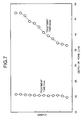
- the anodization treatment was carried out under conditions of different anodization treatment times ranging from 1 to 20 minutes, and the entire surface of the 6-inch wafer was observed thereafter with the field emission type scanning electron microscope.
- Fig. 7 shows the dispersion in the depths of pores of the wafer in the respective treatment times.
- the depths of the pores increase with increase in the treatment time. It was found that when the amount of dissolved hydrogen in the reaction solution 201 in the reaction vessel 300 was not more than 100 ppb, the porous layer having the diameter of pore of 10 nm and the aperture rate of 30% was formed in the thickness of 20 ⁇ m and with the in-plane uniformity of thickness being within the dispersion of ⁇ 3% in the treatment time of one minute.
- the present invention achieved efficient removal of gas molecules of by-product in the chemical reactions in a solution, which no conventional technologies have achieved.
- the present invention permits the chemical reactions in a solution to be carried out with high efficiency, high rate, and high uniformity.
- the present invention allows production of the semiconductor substrate that can be applied to formation of the SOI structure, and the invention also permits the semiconductor substrate in which a light-emitting element or a gas sensor can be made, to be produced from an inexpensive silicon substrate.
Landscapes
- Chemical & Material Sciences (AREA)
- Engineering & Computer Science (AREA)
- Chemical Kinetics & Catalysis (AREA)
- Electrochemistry (AREA)
- Materials Engineering (AREA)
- Metallurgy (AREA)
- Organic Chemistry (AREA)
- Weting (AREA)
- Separation Using Semi-Permeable Membranes (AREA)
Abstract
Description
Claims (47)
- A chemical reaction method, comprising performing a chemical reaction while always controlling the concentration of a gas of a reaction by-product dissolved in a reaction solution in a reaction vessel to be not more than the solubility thereof during the reaction.
- The chemical reaction method according to Claim 1, wherein the reaction solution is circulated outside the reaction vessel, and wherein deaeration of the reaction solution is carried out on the way of circulation.
- The chemical reaction method according to Claim 1, wherein the concentration of the gas is controlled to be not more than 1/10 of the solubility.
- The chemical reaction method according to Claim 1, wherein the concentration of the gas is controlled to be not more than 100 ppb.
- The chemical reaction method according to Claim 1, wherein the reaction by-product is hydrogen.
- The chemical reaction method according to Claim 1, wherein the chemical reaction is an electrochemical reaction.
- The chemical reaction method according to Claim 1, wherein the chemical reaction is an anodization reaction.
- The chemical reaction method according to Claim 7, wherein the anodization reaction is a reaction for forming a porous layer in a surface of a substrate.
- The chemical reaction method according to Claim 8, wherein the substrate is held in the reaction vessel, one surface of the substrate is kept in contact with the reaction solution, the other surface of the substrate is kept in contact with an electrically conductive solution, a negative voltage is applied to the reaction solution, and a positive voltage is applied to the conductive solution.
- The chemical reaction method according to Claim 1, wherein the reaction solution in the reaction vessel is isolated from the atmosphere.
- The chemical reaction method according to Claim 10, wherein the reaction solution is a liquid containing hydrofluoric acid.
- The chemical reaction method according to Claim 8, wherein a surfactant is added into the reaction solution.
- The chemical reaction method according to Claim 12, wherein the surfactant is selected from the group consisting of methanol, ethanol and isopropyl alcohol.
- The chemical reaction method according to Claim 8, wherein the diameters of the pores are not more than 20 nm.
- The chemical reaction method according to Claim 8, wherein the depths of the pores are not less than 20 µm.
- The chemical reaction method according to Claim 8, wherein the aspect ratios of the pores are not less than 1000.
- The chemical reaction method according to Claim 8, wherein the substrate is a silicon wafer.
- The chemical reaction method according to Claim 2, wherein the deaeration is carried out by using a deaerating module comprised of a gas-permeable membrane of hollow fibers and bringing the inside of the hollow fibers into a pressure reduced state with a pump.
- The chemical reaction method according to Claim 2, wherein the deaeration is carried out by using a deaerating module comprised of a gas-permeable membrane of hollow fibers and filling the inside of the hollow fibers with ultrapure water containing no gas at all.
- The chemical reaction method according to Claim 1, wherein fluctuation of the temperature of the reaction solution is controlled within ±0.5°C.
- A chemical reaction apparatus comprising:a reaction vessel having a holding means for holding a substrate, for housing a reaction solution and carrying out a chemical reaction with a substrate therein;a circulation line for circulating the reaction solution outside the reaction vessel;a deaerating device provided on the circulation line, for removing a gas from the reaction solution; anda transferring means for transferring the reaction solution in the circulation line.
- The chemical reaction apparatus according to Claim 21, wherein one surface of the substrate is kept in contact with the reaction solution and the other surface of the substrate is kept in contact with an electrically conductive solution, further comprising an electrode for applying a negative voltage to the reaction solution and an electrode for applying a positive voltage to the electrically conductive solution.
- The chemical reaction apparatus according to Claim 21, wherein the reaction vessel is of a hermetically closed type.
- The chemical reaction apparatus according to Claim 21, wherein the reaction solution is a liquid containing hydrofluoric acid.
- The chemical reaction apparatus according to Claim 21, wherein the deaerating device is constituted in such a manner that in a deaerating module comprised of a gas-permeable membrane of hollow fibers, the inside of the hollow fibers is brought into a pressure reduced stated by a pump.
- The chemical reaction apparatus according to Claim 21, wherein the deaerating device is constituted in such a manner that in a deaerating module comprised of a gas-permeable membrane of hollow fibers, the inside of the hollow fibers is filled with ultrapure water containing no gas at all.
- The chemical reaction apparatus according to Claim 21, wherein means for controlling fluctuation of the temperature of the reaction solution within ±0.5°C is provided on the circulation line.
- A treating method, comprising performing a chemical reaction to treat a body to be treated while always maintaining the concentration of a gas of a reaction by-product dissolved in a reaction solution in contact with the body to be treated in a reaction vessel to be not more than the solubility thereof during the reaction.
- The treating method according to Claim 28, wherein the reaction solution is circulated outside the reaction vessel, and wherein deaeration of the reaction solution is carried out on the way of circulation.
- The treating method according to Claim 28, wherein the concentration of the gas is controlled to be not more than 1/10 of the solubility.
- The treating method according to Claim 28, wherein the concentration of the gas is controlled to be not more than 100 ppb.
- The treating method according to Claim 28, wherein the reaction by-product generated is hydrogen.
- The treating method according to Claim 28, wherein the chemical reaction is an electrochemical reaction.
- The treating method according to Claim 28, wherein the chemical reaction is an anodization reaction.
- The treating method according to Claim 34, wherein the anodization reaction is a reaction for forming a porous layer in a surface of the body to be treated.
- The treating method according to Claim 35, wherein one surface of the body to be treated is kept in contact with the reaction solution, the other surface thereof is kept in contact with an electrically conductive solution, a negative voltage is applied to the reaction solution, and a positive voltage is applied to the conductive solution.
- The treating method according to Claim 28, wherein the reaction solution in the reaction vessel is isolated from the atmosphere.
- The treating method according to Claim 28, wherein the reaction solution is a liquid containing hydrofluoric acid.
- The treating method according to Claim 28, wherein a surfactant is added into the reaction solution.
- The treating method according to Claim 39, wherein the surfactant is selected from the group consisting of methanol, ethanol and isopropyl alcohol.
- The treating method according to Claim 35, wherein the diameters of the pores are not more than 20 nm.
- The treating method according to Claim 35, wherein the depths of the pores are not less than 20 µm.
- The treating method according to Claim 35, wherein the aspect ratios of the pores are not less than 1000.
- The treating method according to Claim 28, wherein the body to be treated is a silicon wafer.
- The treating method according to Claim 28, wherein the deaeration is carried out by using a deaerating module comprised of a gas-permeable membrane of hollow fibers and bringing the inside of the hollow fibers into a pressure reduced state with a pump.
- The treating method according to Claim 28, wherein the deaeration is carried out by using a deaerating module comprised of a gas-permeable membrane of hollow fibers and filling the inside of the hollow fibers with ultrapure water containing no gas at all.
- The treating method according to Claim 28, wherein fluctuation of the temperature of the reaction solution is controlled within ±0.5°C.
Applications Claiming Priority (3)
| Application Number | Priority Date | Filing Date | Title |
|---|---|---|---|
| JP12378397 | 1997-05-14 | ||
| JP123783/97 | 1997-05-14 | ||
| JP12378397A JP3985065B2 (en) | 1997-05-14 | 1997-05-14 | Porous silicon substrate forming method and porous silicon substrate forming apparatus |
Publications (3)
| Publication Number | Publication Date |
|---|---|
| EP0879902A2 true EP0879902A2 (en) | 1998-11-25 |
| EP0879902A3 EP0879902A3 (en) | 1999-12-29 |
| EP0879902B1 EP0879902B1 (en) | 2003-08-13 |
Family
ID=14869193
Family Applications (1)
| Application Number | Title | Priority Date | Filing Date |
|---|---|---|---|
| EP98303765A Expired - Lifetime EP0879902B1 (en) | 1997-05-14 | 1998-05-13 | Treating method and apparatus utilizing chemical reaction |
Country Status (6)
| Country | Link |
|---|---|
| US (1) | US6258244B1 (en) |
| EP (1) | EP0879902B1 (en) |
| JP (1) | JP3985065B2 (en) |
| KR (1) | KR100306839B1 (en) |
| DE (1) | DE69817077T2 (en) |
| TW (1) | TW463219B (en) |
Cited By (5)
| Publication number | Priority date | Publication date | Assignee | Title |
|---|---|---|---|---|
| EP1048757A4 (en) * | 1998-11-09 | 2006-06-14 | Ebara Corp | Plating method and apparatus |
| EP2387458A4 (en) * | 2009-01-15 | 2012-04-11 | Solexel Inc | SYSTEM AND METHOD FOR ELECTRO-ATTACK OF POROUS SILICON |
| CN103276436A (en) * | 2013-06-17 | 2013-09-04 | 天津大学 | Preparation method of novel ordered nano-porous silicon |
| US9076642B2 (en) | 2009-01-15 | 2015-07-07 | Solexel, Inc. | High-Throughput batch porous silicon manufacturing equipment design and processing methods |
| US9401276B2 (en) | 2010-02-12 | 2016-07-26 | Solexel, Inc. | Apparatus for forming porous silicon layers on at least two surfaces of a plurality of silicon templates |
Families Citing this family (21)
| Publication number | Priority date | Publication date | Assignee | Title |
|---|---|---|---|---|
| US7022211B2 (en) | 2000-01-31 | 2006-04-04 | Ebara Corporation | Semiconductor wafer holder and electroplating system for plating a semiconductor wafer |
| EP1229154A4 (en) * | 2000-03-17 | 2006-12-13 | Ebara Corp | Method and apparatus for electroplating |
| JP2002363792A (en) * | 2001-06-01 | 2002-12-18 | Tokyo Electron Ltd | Liquid processing system and liquid processing method |
| JP4821067B2 (en) * | 2001-08-01 | 2011-11-24 | ソニー株式会社 | Anodizing apparatus, method for forming porous layer using the same, and method for producing semiconductor thin film |
| JP2003129283A (en) * | 2001-10-18 | 2003-05-08 | Hitachi Ltd | Plating apparatus and method of manufacturing semiconductor device using the same |
| EP1620903B1 (en) | 2003-04-30 | 2017-08-16 | Cree, Inc. | High-power solid state light emitter package |
| US7005679B2 (en) | 2003-05-01 | 2006-02-28 | Cree, Inc. | Multiple component solid state white light |
| US6972438B2 (en) * | 2003-09-30 | 2005-12-06 | Cree, Inc. | Light emitting diode with porous SiC substrate and method for fabricating |
| EP1969633B1 (en) | 2005-12-22 | 2018-08-29 | Cree, Inc. | Lighting device |
| EP2011164B1 (en) | 2006-04-24 | 2018-08-29 | Cree, Inc. | Side-view surface mount white led |
| US7834367B2 (en) | 2007-01-19 | 2010-11-16 | Cree, Inc. | Low voltage diode with reduced parasitic resistance and method for fabricating |
| US9012937B2 (en) | 2007-10-10 | 2015-04-21 | Cree, Inc. | Multiple conversion material light emitting diode package and method of fabricating same |
| US9431589B2 (en) | 2007-12-14 | 2016-08-30 | Cree, Inc. | Textured encapsulant surface in LED packages |
| US8906218B2 (en) | 2010-05-05 | 2014-12-09 | Solexel, Inc. | Apparatus and methods for uniformly forming porous semiconductor on a substrate |
| EP2427914A4 (en) * | 2009-05-05 | 2013-06-05 | Solexel Inc | HIGH-LEVEL PRODUCTIVITY EQUIPMENT FOR THE MANUFACTURE OF POROUS SEMICONDUCTORS |
| US8992746B2 (en) | 2010-12-02 | 2015-03-31 | Dainippon Screen Mfg. Co., Ltd. | Anodizing apparatus |
| JP6037779B2 (en) * | 2012-11-01 | 2016-12-07 | 株式会社ダルトン | Anodizing apparatus, anodizing system and anodizing method |
| JP6045309B2 (en) * | 2012-11-09 | 2016-12-14 | 株式会社ダルトン | Anodizing apparatus, anodizing system and anodizing method |
| CN104241262B (en) | 2013-06-14 | 2020-11-06 | 惠州科锐半导体照明有限公司 | Light emitting device and display device |
| CN103395740A (en) * | 2013-08-02 | 2013-11-20 | 合肥工业大学 | Method for selectively preparing porous silicon based on silicon on insulator |
| US9799541B1 (en) * | 2014-12-18 | 2017-10-24 | Trutag Technologies, Inc. | Multiple wafer single bath etcher |
Family Cites Families (17)
| Publication number | Priority date | Publication date | Assignee | Title |
|---|---|---|---|---|
| FR2615036B1 (en) | 1987-05-05 | 1989-08-18 | France Etat | MACHINE FOR THE MANUFACTURE OF POROUS SILICON |
| JPH0831460B2 (en) * | 1987-11-13 | 1996-03-27 | 富士通株式会社 | Plating equipment |
| US4891103A (en) | 1988-08-23 | 1990-01-02 | Texas Instruments Incorporated | Anadization system with remote voltage sensing and active feedback control capabilities |
| US5443727A (en) * | 1990-10-30 | 1995-08-22 | Minnesota Mining And Manufacturing Company | Articles having a polymeric shell and method for preparing same |
| JP3347354B2 (en) | 1991-02-15 | 2002-11-20 | キヤノン株式会社 | Etching method and method of manufacturing semiconductor substrate |
| JP3112106B2 (en) | 1991-10-11 | 2000-11-27 | キヤノン株式会社 | Manufacturing method of semiconductor substrate |
| JP2994837B2 (en) | 1992-01-31 | 1999-12-27 | キヤノン株式会社 | Semiconductor substrate flattening method, semiconductor substrate manufacturing method, and semiconductor substrate |
| JP3171903B2 (en) | 1992-01-30 | 2001-06-04 | キヤノン株式会社 | Semiconductor substrate and manufacturing method thereof |
| JP3416163B2 (en) | 1992-01-31 | 2003-06-16 | キヤノン株式会社 | Semiconductor substrate and manufacturing method thereof |
| JP3250673B2 (en) | 1992-01-31 | 2002-01-28 | キヤノン株式会社 | Semiconductor element substrate and method of manufacturing the same |
| JP3261685B2 (en) | 1992-01-31 | 2002-03-04 | キヤノン株式会社 | Semiconductor element substrate and method of manufacturing the same |
| DE69312636T2 (en) * | 1992-11-09 | 1998-02-05 | Canon Kk | Anodizing apparatus with a carrier device for the substrate to be treated |
| US5338416A (en) * | 1993-02-05 | 1994-08-16 | Massachusetts Institute Of Technology | Electrochemical etching process |
| JP3262470B2 (en) | 1993-12-28 | 2002-03-04 | キヤノン株式会社 | Semiconductor substrate and manufacturing method thereof |
| JP3294934B2 (en) | 1994-03-11 | 2002-06-24 | キヤノン株式会社 | Method for manufacturing semiconductor substrate and semiconductor substrate |
| US5464509A (en) * | 1994-05-20 | 1995-11-07 | Massachusetts Institute Of Technology | P-N junction etch-stop technique for electrochemical etching of semiconductors |
| JP2979963B2 (en) | 1994-07-21 | 1999-11-22 | 日本電池株式会社 | Rechargeable battery |
-
1997
- 1997-05-14 JP JP12378397A patent/JP3985065B2/en not_active Expired - Fee Related
-
1998
- 1998-05-13 US US09/076,834 patent/US6258244B1/en not_active Expired - Lifetime
- 1998-05-13 EP EP98303765A patent/EP0879902B1/en not_active Expired - Lifetime
- 1998-05-13 DE DE69817077T patent/DE69817077T2/en not_active Expired - Lifetime
- 1998-05-14 TW TW087107467A patent/TW463219B/en active
- 1998-05-14 KR KR1019980017312A patent/KR100306839B1/en not_active Expired - Fee Related
Cited By (6)
| Publication number | Priority date | Publication date | Assignee | Title |
|---|---|---|---|---|
| EP1048757A4 (en) * | 1998-11-09 | 2006-06-14 | Ebara Corp | Plating method and apparatus |
| US7118664B2 (en) | 1998-11-09 | 2006-10-10 | Ebara Corporation | Plating method and apparatus |
| EP2387458A4 (en) * | 2009-01-15 | 2012-04-11 | Solexel Inc | SYSTEM AND METHOD FOR ELECTRO-ATTACK OF POROUS SILICON |
| US9076642B2 (en) | 2009-01-15 | 2015-07-07 | Solexel, Inc. | High-Throughput batch porous silicon manufacturing equipment design and processing methods |
| US9401276B2 (en) | 2010-02-12 | 2016-07-26 | Solexel, Inc. | Apparatus for forming porous silicon layers on at least two surfaces of a plurality of silicon templates |
| CN103276436A (en) * | 2013-06-17 | 2013-09-04 | 天津大学 | Preparation method of novel ordered nano-porous silicon |
Also Published As
| Publication number | Publication date |
|---|---|
| JP3985065B2 (en) | 2007-10-03 |
| KR100306839B1 (en) | 2001-10-19 |
| EP0879902B1 (en) | 2003-08-13 |
| DE69817077D1 (en) | 2003-09-18 |
| TW463219B (en) | 2001-11-11 |
| KR19980087032A (en) | 1998-12-05 |
| DE69817077T2 (en) | 2004-06-03 |
| JPH10312990A (en) | 1998-11-24 |
| EP0879902A3 (en) | 1999-12-29 |
| US6258244B1 (en) | 2001-07-10 |
Similar Documents
| Publication | Publication Date | Title |
|---|---|---|
| US6258244B1 (en) | Treating method and apparatus utilizing chemical reaction | |
| KR100287502B1 (en) | Semiconductor processing system and substrate processing system | |
| KR100385255B1 (en) | Method of cleaning porous body, and process for producing porous body, non-porous film or bonded substrate | |
| US5635053A (en) | Method and apparatus for cleaning electronic parts | |
| US6547938B1 (en) | Anodizing apparatus, utilizing a perforated negative electrode | |
| US20030008473A1 (en) | Anodizing method and apparatus and semiconductor substrate manufacturing method | |
| KR100504413B1 (en) | Apparatus and method for etching a dielectric layer over a semiconductor substrate | |
| JP3455035B2 (en) | Electrolytic ionic water generation device and semiconductor manufacturing device | |
| JP3313263B2 (en) | Electrolytic water generation method, its generation apparatus, and semiconductor manufacturing apparatus | |
| JPH1064870A (en) | Method for cleaning porous surface and method for cleaning semiconductor surface | |
| KR20140061287A (en) | Apparatus and methods for uniformly forming porous semiconductor on a substrate | |
| CN106796963A (en) | Method and apparatus for forming porous silicon layer | |
| JP3639102B2 (en) | Wet processing equipment | |
| JP3416190B2 (en) | Anodizing apparatus and method | |
| JP3437716B2 (en) | Semiconductor substrate cleaning method and cleaning apparatus used therefor | |
| US20040124088A1 (en) | Processing apparatus | |
| KR100202761B1 (en) | Cleaning method of semiconductor substrate and apparatus thereof | |
| JP2005244089A (en) | Anodizing apparatus, processing method, and method for manufacturing semiconductor substrate | |
| JPH05198557A (en) | Anodizing device | |
| JP2006066728A (en) | Substrate processing apparatus and method | |
| JP2004214237A (en) | Treatment apparatus | |
| JP2004211111A (en) | Processing equipment | |
| JP2000133632A (en) | Method for etching porous body and apparatus for etching porous body | |
| JP2004214238A (en) | Treatment apparatus | |
| JP2007194346A (en) | Semiconductor manufacturing method and manufacturing apparatus thereof |
Legal Events
| Date | Code | Title | Description |
|---|---|---|---|
| PUAI | Public reference made under article 153(3) epc to a published international application that has entered the european phase |
Free format text: ORIGINAL CODE: 0009012 |
|
| AK | Designated contracting states |
Kind code of ref document: A2 Designated state(s): DE ES FR GB NL |
|
| AX | Request for extension of the european patent |
Free format text: AL;LT;LV;MK;RO;SI |
|
| PUAL | Search report despatched |
Free format text: ORIGINAL CODE: 0009013 |
|
| AK | Designated contracting states |
Kind code of ref document: A3 Designated state(s): AT BE CH CY DE DK ES FI FR GB GR IE IT LI LU MC NL PT SE |
|
| AX | Request for extension of the european patent |
Free format text: AL;LT;LV;MK;RO;SI |
|
| 17P | Request for examination filed |
Effective date: 20000515 |
|
| AKX | Designation fees paid |
Free format text: DE ES FR GB NL |
|
| 17Q | First examination report despatched |
Effective date: 20020320 |
|
| GRAH | Despatch of communication of intention to grant a patent |
Free format text: ORIGINAL CODE: EPIDOS IGRA |
|
| GRAH | Despatch of communication of intention to grant a patent |
Free format text: ORIGINAL CODE: EPIDOS IGRA |
|
| GRAA | (expected) grant |
Free format text: ORIGINAL CODE: 0009210 |
|
| AK | Designated contracting states |
Designated state(s): DE ES FR GB NL |
|
| PG25 | Lapsed in a contracting state [announced via postgrant information from national office to epo] |
Ref country code: NL Free format text: LAPSE BECAUSE OF FAILURE TO SUBMIT A TRANSLATION OF THE DESCRIPTION OR TO PAY THE FEE WITHIN THE PRESCRIBED TIME-LIMIT Effective date: 20030813 |
|
| REG | Reference to a national code |
Ref country code: GB Ref legal event code: FG4D |
|
| REF | Corresponds to: |
Ref document number: 69817077 Country of ref document: DE Date of ref document: 20030918 Kind code of ref document: P |
|
| PG25 | Lapsed in a contracting state [announced via postgrant information from national office to epo] |
Ref country code: ES Free format text: LAPSE BECAUSE OF FAILURE TO SUBMIT A TRANSLATION OF THE DESCRIPTION OR TO PAY THE FEE WITHIN THE PRESCRIBED TIME-LIMIT Effective date: 20031124 |
|
| NLV1 | Nl: lapsed or annulled due to failure to fulfill the requirements of art. 29p and 29m of the patents act | ||
| ET | Fr: translation filed | ||
| PLBE | No opposition filed within time limit |
Free format text: ORIGINAL CODE: 0009261 |
|
| STAA | Information on the status of an ep patent application or granted ep patent |
Free format text: STATUS: NO OPPOSITION FILED WITHIN TIME LIMIT |
|
| 26N | No opposition filed |
Effective date: 20040514 |
|
| PGFP | Annual fee paid to national office [announced via postgrant information from national office to epo] |
Ref country code: GB Payment date: 20140507 Year of fee payment: 17 |
|
| PGFP | Annual fee paid to national office [announced via postgrant information from national office to epo] |
Ref country code: DE Payment date: 20140507 Year of fee payment: 17 Ref country code: FR Payment date: 20140509 Year of fee payment: 17 |
|
| REG | Reference to a national code |
Ref country code: DE Ref legal event code: R119 Ref document number: 69817077 Country of ref document: DE |
|
| GBPC | Gb: european patent ceased through non-payment of renewal fee |
Effective date: 20150513 |
|
| REG | Reference to a national code |
Ref country code: FR Ref legal event code: ST Effective date: 20160129 |
|
| PG25 | Lapsed in a contracting state [announced via postgrant information from national office to epo] |
Ref country code: GB Free format text: LAPSE BECAUSE OF NON-PAYMENT OF DUE FEES Effective date: 20150513 Ref country code: DE Free format text: LAPSE BECAUSE OF NON-PAYMENT OF DUE FEES Effective date: 20151201 |
|
| PG25 | Lapsed in a contracting state [announced via postgrant information from national office to epo] |
Ref country code: FR Free format text: LAPSE BECAUSE OF NON-PAYMENT OF DUE FEES Effective date: 20150601 |