EP0880077B1 - Procédé et appareil pour fabriquer un micro-dispositif - Google Patents
Procédé et appareil pour fabriquer un micro-dispositif Download PDFInfo
- Publication number
- EP0880077B1 EP0880077B1 EP98303499A EP98303499A EP0880077B1 EP 0880077 B1 EP0880077 B1 EP 0880077B1 EP 98303499 A EP98303499 A EP 98303499A EP 98303499 A EP98303499 A EP 98303499A EP 0880077 B1 EP0880077 B1 EP 0880077B1
- Authority
- EP
- European Patent Office
- Prior art keywords
- mask
- hinged
- layer
- mems device
- several layers
- Prior art date
- Legal status (The legal status is an assumption and is not a legal conclusion. Google has not performed a legal analysis and makes no representation as to the accuracy of the status listed.)
- Expired - Lifetime
Links
- 238000000034 method Methods 0.000 title claims description 17
- 239000000463 material Substances 0.000 claims description 8
- 238000000059 patterning Methods 0.000 claims description 8
- 230000003287 optical effect Effects 0.000 claims description 2
- 238000000206 photolithography Methods 0.000 claims 1
- 239000000758 substrate Substances 0.000 description 11
- 150000001875 compounds Chemical class 0.000 description 7
- 238000000151 deposition Methods 0.000 description 3
- 238000004519 manufacturing process Methods 0.000 description 3
- 238000012805 post-processing Methods 0.000 description 3
- 238000010586 diagram Methods 0.000 description 2
- 238000004518 low pressure chemical vapour deposition Methods 0.000 description 2
- 229910021420 polycrystalline silicon Inorganic materials 0.000 description 2
- 229920005591 polysilicon Polymers 0.000 description 2
- 229910052581 Si3N4 Inorganic materials 0.000 description 1
- VYPSYNLAJGMNEJ-UHFFFAOYSA-N Silicium dioxide Chemical compound O=[Si]=O VYPSYNLAJGMNEJ-UHFFFAOYSA-N 0.000 description 1
- 239000002253 acid Substances 0.000 description 1
- 230000015572 biosynthetic process Effects 0.000 description 1
- 238000005530 etching Methods 0.000 description 1
- 238000001459 lithography Methods 0.000 description 1
- 229920002120 photoresistant polymer Polymers 0.000 description 1
- 238000002360 preparation method Methods 0.000 description 1
- HQVNEWCFYHHQES-UHFFFAOYSA-N silicon nitride Chemical compound N12[Si]34N5[Si]62N3[Si]51N64 HQVNEWCFYHHQES-UHFFFAOYSA-N 0.000 description 1
- 229910052814 silicon oxide Inorganic materials 0.000 description 1
- 238000001039 wet etching Methods 0.000 description 1
Images





Classifications
-
- G—PHYSICS
- G03—PHOTOGRAPHY; CINEMATOGRAPHY; ANALOGOUS TECHNIQUES USING WAVES OTHER THAN OPTICAL WAVES; ELECTROGRAPHY; HOLOGRAPHY
- G03F—PHOTOMECHANICAL PRODUCTION OF TEXTURED OR PATTERNED SURFACES, e.g. FOR PRINTING, FOR PROCESSING OF SEMICONDUCTOR DEVICES; MATERIALS THEREFOR; ORIGINALS THEREFOR; APPARATUS SPECIALLY ADAPTED THEREFOR
- G03F9/00—Registration or positioning of originals, masks, frames, photographic sheets or textured or patterned surfaces, e.g. automatically
-
- C—CHEMISTRY; METALLURGY
- C23—COATING METALLIC MATERIAL; COATING MATERIAL WITH METALLIC MATERIAL; CHEMICAL SURFACE TREATMENT; DIFFUSION TREATMENT OF METALLIC MATERIAL; COATING BY VACUUM EVAPORATION, BY SPUTTERING, BY ION IMPLANTATION OR BY CHEMICAL VAPOUR DEPOSITION, IN GENERAL; INHIBITING CORROSION OF METALLIC MATERIAL OR INCRUSTATION IN GENERAL
- C23C—COATING METALLIC MATERIAL; COATING MATERIAL WITH METALLIC MATERIAL; SURFACE TREATMENT OF METALLIC MATERIAL BY DIFFUSION INTO THE SURFACE, BY CHEMICAL CONVERSION OR SUBSTITUTION; COATING BY VACUUM EVAPORATION, BY SPUTTERING, BY ION IMPLANTATION OR BY CHEMICAL VAPOUR DEPOSITION, IN GENERAL
- C23C14/00—Coating by vacuum evaporation, by sputtering or by ion implantation of the coating forming material
- C23C14/04—Coating on selected surface areas, e.g. using masks
- C23C14/042—Coating on selected surface areas, e.g. using masks using masks
Definitions
- the present invention relates generally to a method and apparatus for making micro mechanical or micro electro mechanical devices.
- Micro electro mechanical systems (MEMS) devices are typically fabricated by depositing a plurality of materials layers, some of which are then removed by selective etching during a release procedure.
- MEMS device manufacture often requires depositing additional patterned films or layers upon a portion of the MEMS device after the initially deposited layers have been released. Such post processing is occasioned due to the limitations imposed on film materials selection by the etchant, typically acid, used in the release.
- a hinged mask that is rotatable 180° about the hinge is used as a micro-sized shadow mask to deposit a patterned film of arbitrary composition on a released MEMS device.
- the hinged mask is formed coincidently with the pre-released MEMS device.
- Suitably placed openings or bores are formed in the mask.
- the openings define a pattern that is transferable in the form of a patterned layer that is deposited on the released MEMS device. Since the hinged plate is formed by the original lithography, i.e., simultaneously with the films forming the pre-released MEMS device, it can be aligned to the MEMS device with a high degree of accuracy.
- the hinged mask is rotated about the hinge and placed over the MEMS device.
- a patterned layer is directly deposited on the MEMS device.
- the mask is then rotated away from the MEMS device, allowing, as the application dictates, one or more additional masks to be sequentially rotated into position above the MEMS device and additional patterned layers to be deposited.
- FIG. 1 is a perspective view of an exemplary embodiment of a micro-hinge 2 suitable for use in conjunction with the present invention.
- the micro-hinge 2 includes a plate 4, a hinge pin 6 and a staple 8.
- the micro-hinge 2 is hinged to a substrate 14.
- the staple 8 is attached to the substrate 14 at contact points 10 and 12.
- the staple 8 and hinge pin 6 are suitably fabricated so that the plate 4 is substantially free to rotate up to and including 180° off the substrate 14.
- the micro-hinge 2 can be formed via a three-mask double-layer polysilicon process with oxide sacrificial layers using low-pressure chemical vapor deposition (LPCVD). See, Pister et al., "Microfabricated Hinges,” v. 33, Sensors and Actuators A, pp. 249-256, 1992.
- LPCVD low-pressure chemical vapor deposition
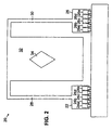
- FIG. 2 shows an exemplary embodiment of a hinged mask 20 according to the present invention.
- the exemplary hinged mask 20 includes two compound hinges 22, 26, a mask 32 and opening 34. Arms 28 and 30 connect respective compound hinges 22 and 26 to the mask 32.
- the compound hinges 22, 26 consist of respective pluralities of micro-hinges 24a-e and 26a-e.
- the structure of micro-hinges 24a-e and 26a-e are adapted from the micro-hinge 2 illustrated in FIG. 1.
- a plurality of such micro-hinges are used in preference to a single micro-hinge to improve robustness.
- Other configurations of compound hinges for such "heavy-duty"service based on the simple exemplary micro-hinge 2 shown in FIG. 2, may suitably be used.
- the compound hinges 22 and 26 may be directly attached to the mask 32 so that arms 28 and 30 are not required.
- the opening 34 is suitably configured for transferring a desired pattern to the surface of a released MEMS device. It will be appreciated that more than one opening 34 can be included in the mask as appropriate to pattern a layer into a particular configuration.
- the compound hinges 22, 26, arms 28, 30 and mask 32 can be formed of polysilicon, silicon nitride, silicon oxide and other materials typically used for MEMS device manufacture.
- the exemplary hinged mask 20 of FIG. 2 can be used in a method according to the present invention for fabricating a MEMS device.
- An exemplary method for such purpose is illustrated by flow-diagram in FIG. 3.
- one or more hinged masks are formed during photolithographic patterning of a MEMS device. Formation of the hinged masks during MEMS patterning advantageously provides for precision alignment of the hinged masks to the MEMS device.
- a hinged mask is rotated out-of-plane of the substrate or wafer through approximately 180° (nearly back in-the-plane) to lay on top of the released MEMS device, as noted in operation block 44.
- Electrostatic, magnetic or mechanical instrumentalities can be used to rotate the hinged mask into position.
- Optional locking members suitable for locking the hinged masks in position can be provided.
- such a locking member is configured as a flexible beam, attached to the substrate at one end. The locking member is positioned on the substrate so that a portion of the free end of the locking member can be positioned on top of a hinged mask that has been rotated in position.
- the flexion in the beam as a result of positioning it on top of the hinged mask provides a biasing force that substantially prevents the hinged mask from moving.
- a dry pattern transfer of the pattern defined by the mask is performed, as indicated in block 48. It will be readily apparent to those skilled in the art that the hinged mask is functioning as a shadow mask. Dry pattern transfer via shadow mask is old in the art. Since wet etching is avoided, a wide variety of materials may be deposited on the MEMS device.
- the hinged mask is rotated away from the MEMS device and preferably back to its original position in-the-plane of the substrate after pattern transfer. If additional hinged masks are present for pattern transfer, they are sequentially rotated into place for patterning.
- the present method advantageously provides the ability to place a virtually unlimited variety of structures capable of a wide range of functions on a released MEMS device.
- Several nonlimiting examples of such structures include, dielectric mirrors, dielectric filters, polarizers, devices having a nonlinear optical response such as frequency doublers, and the like.
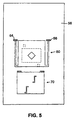
- FIGS. 4 - 8 show an exemplary arrangement comprising two hinged masks and a released MEMS device, and illustrate the use of such masks according to the aforedescribed for depositing additional structure onto the MEMS device.
- FIG. 4 shows a first hinged mask 60 with opening 62, a second hinged mask 70 with openings 72 and a released MEMS device 80.
- the first and second hinged masks 60, 70 are rotatably attached to a substrate 58 at respective compound hinges 64, 66 and 74, 76.
- the first hinged mask 60 is rotated out of the plane of the substrate 58 towards the MEMS device 80.
- FIG. 5 shows the first hinged mask 60 lying directly over the MEMS device.
- FIG. 6 shows the MEMS device 80 after dry pattern transfer of the patterned layer 82 and after the first hinged mask 60 has been rotated away from the MEMS device and back in to the plane of the substrate 58.
- FIG. 7 shows the second hinged mask 70 lying directly over the MEMS device.
- FIG. 8 shows the MEMS device 80 after the second dry pattern transfer by which patterned layer 84 is added to the MEMS device 80.
- the second hinged mask 70 is shown rotated away from the MEMS device and in the plane of the substrate 58 in FIG. 8.
Landscapes
- Chemical & Material Sciences (AREA)
- Mechanical Engineering (AREA)
- General Physics & Mathematics (AREA)
- Chemical Kinetics & Catalysis (AREA)
- Engineering & Computer Science (AREA)
- Materials Engineering (AREA)
- Physics & Mathematics (AREA)
- Metallurgy (AREA)
- Organic Chemistry (AREA)
- Micromachines (AREA)
- Mechanical Light Control Or Optical Switches (AREA)
- Preparing Plates And Mask In Photomechanical Process (AREA)
- Physical Vapour Deposition (AREA)
Claims (11)
- Article de système micro-électromécanique comprenant un masque articulé (20), comprenant :dans lequel une première couche ayant le motif prédéterminé est formée sur la surface lorsqu'un premier matériau est fourni de manière convenable au masque.une charnière (22, 26) connectée à un support ; etun masque (32) ayant une ouverture (34) définissant un motif prédéterminé pour le transfert sur une surface, le masque étant connecté en rotation à la charnière,
- Article selon la revendication 1, dans lequel la surface est un dispositif de système micro-électromécanique ayant subi l'étape de libération.
- Article selon la revendication 2, comprenant en outre le dispositif de système micro-électromécanique ayant subi l'étape de libération.
- Article selon la revendication 1, dans lequel en outre le masque (32) peut tourner sur 180° à l'intérieur de la charnière.
- Article selon la revendication 1, dans lequel en outre une seconde couche, et d'autres, d'un premier matériau, et d'autres, sont reproduites à la surface, lesdites couches, première, seconde et autres, formant collectivement des structures sélectionnées dans un groupe composé de miroirs diélectriques, de filtres diélectriques, de polariseurs et de dispositifs ayant une réponse optique non linéaire.
- Procédé de formation d'un micro-dispositif de systèmes électromécaniques, comprenant les étapes consistant à :former (40) sur un support un masque articulé et plusieurs couches du micro-dispositif de systèmes électromécaniques ;libérer le masque articulé et la pluralité de couches ;tourner (44) le masque articulé pour l'éloigner du support et le rapprocher de la pluralité de couches ; etgraver à sec (48) une première couche de matériau sur une couche supérieure de la pluralité de couches.
- Procédé selon la revendication 6, comprenant en outre l'étape consistant à :tourner le masque articulé pour l'éloigner de la pluralité de couches après la gravure sèche de la première couche.
- Procédé selon la revendication 6, dans lequel l'étape de rotation comprend en outre le fait de tourner le masque articulé d'environ 180°.
- Procédé selon la revendication 6, dans lequel l'étape de formation comprend en outre l'usage de la photolithographie pour former le masque articulé et la pluralité de couches.
- Procédé selon la revendication 9, dans lequel l'étape de libération comprend l'usage d'un agent de gravure.
- Procédé selon la revendication 6 dans lequel l'étape de gravure sèche comprend en outre la gravure sèche de la première couche, afin qu'elle ait un première indice de réfraction, et comprend en outre l'étape de gravure sèche d'une seconde couche de matériau sur la première couche, la seconde couche ayant un second indice de réfraction, le premier et le second indice de réfraction différant suffisamment l'un de l'autre pour que la première et la seconde couche puissent fonctionner comme un filtre destiné à être utilisé pour réfléchir une lumière ayant une longueur d'onde spécifique et laisser passer la lumière ayant d'autres longueurs d'onde.
Applications Claiming Priority (2)
| Application Number | Priority Date | Filing Date | Title |
|---|---|---|---|
| US856565 | 1997-05-15 | ||
| US08/856,565 US5912094A (en) | 1997-05-15 | 1997-05-15 | Method and apparatus for making a micro device |
Publications (3)
| Publication Number | Publication Date |
|---|---|
| EP0880077A2 EP0880077A2 (fr) | 1998-11-25 |
| EP0880077A3 EP0880077A3 (fr) | 2003-05-14 |
| EP0880077B1 true EP0880077B1 (fr) | 2005-01-05 |
Family
ID=25323963
Family Applications (1)
| Application Number | Title | Priority Date | Filing Date |
|---|---|---|---|
| EP98303499A Expired - Lifetime EP0880077B1 (fr) | 1997-05-15 | 1998-05-05 | Procédé et appareil pour fabriquer un micro-dispositif |
Country Status (4)
| Country | Link |
|---|---|
| US (1) | US5912094A (fr) |
| EP (1) | EP0880077B1 (fr) |
| JP (1) | JP3808205B2 (fr) |
| DE (1) | DE69828461T2 (fr) |
Families Citing this family (51)
| Publication number | Priority date | Publication date | Assignee | Title |
|---|---|---|---|---|
| US5994159A (en) * | 1997-12-22 | 1999-11-30 | Lucent Technologies, Inc. | Self-assemblying micro-mechanical device |
| US6872984B1 (en) | 1998-07-29 | 2005-03-29 | Silicon Light Machines Corporation | Method of sealing a hermetic lid to a semiconductor die at an angle |
| US6303986B1 (en) | 1998-07-29 | 2001-10-16 | Silicon Light Machines | Method of and apparatus for sealing an hermetic lid to a semiconductor die |
| US6753638B2 (en) * | 2000-02-03 | 2004-06-22 | Calient Networks, Inc. | Electrostatic actuator for micromechanical systems |
| US6956878B1 (en) | 2000-02-07 | 2005-10-18 | Silicon Light Machines Corporation | Method and apparatus for reducing laser speckle using polarization averaging |
| US20010050828A1 (en) | 2000-05-18 | 2001-12-13 | Davis Michael W. | Reverse flow disk drive and head suspension for same |
| US7259510B1 (en) | 2000-08-30 | 2007-08-21 | Agere Systems Inc. | On-chip vacuum tube device and process for making device |
| US6708491B1 (en) | 2000-09-12 | 2004-03-23 | 3M Innovative Properties Company | Direct acting vertical thermal actuator |
| US6531947B1 (en) | 2000-09-12 | 2003-03-11 | 3M Innovative Properties Company | Direct acting vertical thermal actuator with controlled bending |
| US6483419B1 (en) | 2000-09-12 | 2002-11-19 | 3M Innovative Properties Company | Combination horizontal and vertical thermal actuator |
| US6825967B1 (en) | 2000-09-29 | 2004-11-30 | Calient Networks, Inc. | Shaped electrodes for micro-electro-mechanical-system (MEMS) devices to improve actuator performance and methods for fabricating the same |
| US7177081B2 (en) | 2001-03-08 | 2007-02-13 | Silicon Light Machines Corporation | High contrast grating light valve type device |
| US6707591B2 (en) | 2001-04-10 | 2004-03-16 | Silicon Light Machines | Angled illumination for a single order light modulator based projection system |
| US6438954B1 (en) | 2001-04-27 | 2002-08-27 | 3M Innovative Properties Company | Multi-directional thermal actuator |
| US6543087B2 (en) | 2001-06-01 | 2003-04-08 | Aip Networks, Inc. | Micro-electromechanical hinged flap structure |
| US6865346B1 (en) | 2001-06-05 | 2005-03-08 | Silicon Light Machines Corporation | Fiber optic transceiver |
| US6747781B2 (en) | 2001-06-25 | 2004-06-08 | Silicon Light Machines, Inc. | Method, apparatus, and diffuser for reducing laser speckle |
| US6782205B2 (en) | 2001-06-25 | 2004-08-24 | Silicon Light Machines | Method and apparatus for dynamic equalization in wavelength division multiplexing |
| US6829092B2 (en) | 2001-08-15 | 2004-12-07 | Silicon Light Machines, Inc. | Blazed grating light valve |
| US6930364B2 (en) * | 2001-09-13 | 2005-08-16 | Silicon Light Machines Corporation | Microelectronic mechanical system and methods |
| US6989603B2 (en) * | 2001-10-02 | 2006-01-24 | Guobiao Zhang | nF-Opening Aiv Structures |
| US6956995B1 (en) | 2001-11-09 | 2005-10-18 | Silicon Light Machines Corporation | Optical communication arrangement |
| US6800238B1 (en) | 2002-01-15 | 2004-10-05 | Silicon Light Machines, Inc. | Method for domain patterning in low coercive field ferroelectrics |
| US6728023B1 (en) | 2002-05-28 | 2004-04-27 | Silicon Light Machines | Optical device arrays with optimized image resolution |
| US6767751B2 (en) * | 2002-05-28 | 2004-07-27 | Silicon Light Machines, Inc. | Integrated driver process flow |
| US7054515B1 (en) | 2002-05-30 | 2006-05-30 | Silicon Light Machines Corporation | Diffractive light modulator-based dynamic equalizer with integrated spectral monitor |
| US6822797B1 (en) | 2002-05-31 | 2004-11-23 | Silicon Light Machines, Inc. | Light modulator structure for producing high-contrast operation using zero-order light |
| US6829258B1 (en) | 2002-06-26 | 2004-12-07 | Silicon Light Machines, Inc. | Rapidly tunable external cavity laser |
| US6908201B2 (en) | 2002-06-28 | 2005-06-21 | Silicon Light Machines Corporation | Micro-support structures |
| US6813059B2 (en) | 2002-06-28 | 2004-11-02 | Silicon Light Machines, Inc. | Reduced formation of asperities in contact micro-structures |
| US6714337B1 (en) | 2002-06-28 | 2004-03-30 | Silicon Light Machines | Method and device for modulating a light beam and having an improved gamma response |
| US6801354B1 (en) | 2002-08-20 | 2004-10-05 | Silicon Light Machines, Inc. | 2-D diffraction grating for substantially eliminating polarization dependent losses |
| US7057795B2 (en) | 2002-08-20 | 2006-06-06 | Silicon Light Machines Corporation | Micro-structures with individually addressable ribbon pairs |
| US6712480B1 (en) | 2002-09-27 | 2004-03-30 | Silicon Light Machines | Controlled curvature of stressed micro-structures |
| US6928207B1 (en) | 2002-12-12 | 2005-08-09 | Silicon Light Machines Corporation | Apparatus for selectively blocking WDM channels |
| US6987600B1 (en) | 2002-12-17 | 2006-01-17 | Silicon Light Machines Corporation | Arbitrary phase profile for better equalization in dynamic gain equalizer |
| US7057819B1 (en) | 2002-12-17 | 2006-06-06 | Silicon Light Machines Corporation | High contrast tilting ribbon blazed grating |
| US6934070B1 (en) | 2002-12-18 | 2005-08-23 | Silicon Light Machines Corporation | Chirped optical MEM device |
| US6927891B1 (en) | 2002-12-23 | 2005-08-09 | Silicon Light Machines Corporation | Tilt-able grating plane for improved crosstalk in 1×N blaze switches |
| US7068372B1 (en) | 2003-01-28 | 2006-06-27 | Silicon Light Machines Corporation | MEMS interferometer-based reconfigurable optical add-and-drop multiplexor |
| US7286764B1 (en) | 2003-02-03 | 2007-10-23 | Silicon Light Machines Corporation | Reconfigurable modulator-based optical add-and-drop multiplexer |
| US6947613B1 (en) | 2003-02-11 | 2005-09-20 | Silicon Light Machines Corporation | Wavelength selective switch and equalizer |
| US6922272B1 (en) | 2003-02-14 | 2005-07-26 | Silicon Light Machines Corporation | Method and apparatus for leveling thermal stress variations in multi-layer MEMS devices |
| US6922273B1 (en) | 2003-02-28 | 2005-07-26 | Silicon Light Machines Corporation | PDL mitigation structure for diffractive MEMS and gratings |
| US7027202B1 (en) | 2003-02-28 | 2006-04-11 | Silicon Light Machines Corp | Silicon substrate as a light modulator sacrificial layer |
| US7391973B1 (en) | 2003-02-28 | 2008-06-24 | Silicon Light Machines Corporation | Two-stage gain equalizer |
| US6806997B1 (en) | 2003-02-28 | 2004-10-19 | Silicon Light Machines, Inc. | Patterned diffractive light modulator ribbon for PDL reduction |
| US6829077B1 (en) | 2003-02-28 | 2004-12-07 | Silicon Light Machines, Inc. | Diffractive light modulator with dynamically rotatable diffraction plane |
| US7042611B1 (en) | 2003-03-03 | 2006-05-09 | Silicon Light Machines Corporation | Pre-deflected bias ribbons |
| US8330128B2 (en) * | 2009-04-17 | 2012-12-11 | Varian Semiconductor Equipment Associates, Inc. | Implant mask with moveable hinged mask segments |
| US12103843B2 (en) | 2021-01-20 | 2024-10-01 | Calient.Ai Inc. | MEMS mirror arrays with reduced crosstalk |
Family Cites Families (3)
| Publication number | Priority date | Publication date | Assignee | Title |
|---|---|---|---|---|
| US4575229A (en) * | 1984-05-03 | 1986-03-11 | Koltron Corporation | Photoetch plate hinge |
| US4698284A (en) * | 1985-10-25 | 1987-10-06 | M&T Chemicals Inc. | Device for aligning a photomask onto a printed wiring board |
| US5726480A (en) * | 1995-01-27 | 1998-03-10 | The Regents Of The University Of California | Etchants for use in micromachining of CMOS Microaccelerometers and microelectromechanical devices and method of making the same |
-
1997
- 1997-05-15 US US08/856,565 patent/US5912094A/en not_active Expired - Lifetime
-
1998
- 1998-05-05 DE DE69828461T patent/DE69828461T2/de not_active Expired - Lifetime
- 1998-05-05 EP EP98303499A patent/EP0880077B1/fr not_active Expired - Lifetime
- 1998-05-15 JP JP13289398A patent/JP3808205B2/ja not_active Expired - Fee Related
Also Published As
| Publication number | Publication date |
|---|---|
| JP3808205B2 (ja) | 2006-08-09 |
| DE69828461D1 (de) | 2005-02-10 |
| US5912094A (en) | 1999-06-15 |
| EP0880077A2 (fr) | 1998-11-25 |
| JPH1138591A (ja) | 1999-02-12 |
| EP0880077A3 (fr) | 2003-05-14 |
| DE69828461T2 (de) | 2005-12-15 |
Similar Documents
| Publication | Publication Date | Title |
|---|---|---|
| EP0880077B1 (fr) | Procédé et appareil pour fabriquer un micro-dispositif | |
| EP1485758B1 (fr) | Procede pour fabriquer une structure destinee a un dispositif a systemes microelectromecaniques (mems) | |
| KR100968160B1 (ko) | 광학 소자 및 광학 소자의 제조방법 | |
| CN105353506B (zh) | 垂直梳齿驱动moems微镜及其制作方法 | |
| JP4056559B2 (ja) | マイクロ機械加工構造物の製法およびかかる方法を使用して製造されたマイクロ機械加工構造物 | |
| EP1510848B1 (fr) | Modulateur spatial de lumière utilisant un actuateur circuit intégré et sa méthode de fabrication | |
| CA2149932A1 (fr) | Faconnage d'espaceurs sacrificiels pour dispositifs micromecaniques | |
| WO2008122865A2 (fr) | Micro-miroir de microsystème électromécanique | |
| CA2137063A1 (fr) | Modulateur micromecanique | |
| WO2014010593A1 (fr) | Marque, son procédé de formation et appareil d'exposition | |
| US6790698B2 (en) | Process for integrating dielectric optical coatings into micro-electromechanical devices | |
| EP2562572A1 (fr) | Procédé pour la fabrication d'un opercule pelliculaire | |
| JP4794092B2 (ja) | 光学memsコンポーネントの製造方法 | |
| US6902871B2 (en) | Method for manufacturing polymer microstructures and polymer waveguides | |
| EP1093003B1 (fr) | Appareil optique micro-électromécanique | |
| US7785913B2 (en) | System and method for forming moveable features on a composite substrate | |
| EP1211726B1 (fr) | Ruban articulé en silicium monocristallin pour micro-miroir et MEMS sur matériau SOI | |
| US6297069B1 (en) | Method for supporting during fabrication mechanical members of semi-conductive dies, wafers, and devices and an associated intermediate device assembly | |
| AU765894B2 (en) | Methods of fabricating etched structures | |
| KR102343227B1 (ko) | 각감응성 분광 필터 및 바이모르프 회전 구동기를 포함하는 가변 분광 필터 모듈 | |
| Klemic et al. | Fabrication issues in micromachined tunable optical filters | |
| CN118083904A (zh) | 微机电器件的制作方法、及微机电器件 | |
| JP4016223B2 (ja) | 蒸着膜形成方法 | |
| Jeong et al. | Tunable optical bandpass filter with high-quality vertical mirrors microassembled on movable MEMS platforms | |
| Ostrow II et al. | Novel microelectromechanical systems image reversal fabrication process based on robust SU-8 masking layers |
Legal Events
| Date | Code | Title | Description |
|---|---|---|---|
| PUAI | Public reference made under article 153(3) epc to a published international application that has entered the european phase |
Free format text: ORIGINAL CODE: 0009012 |
|
| AK | Designated contracting states |
Kind code of ref document: A2 Designated state(s): AT BE CH CY DE DK ES FI FR GB GR IE IT LI LU MC NL PT SE |
|
| AX | Request for extension of the european patent |
Free format text: AL;LT;LV;MK;RO;SI |
|
| PUAL | Search report despatched |
Free format text: ORIGINAL CODE: 0009013 |
|
| RIC1 | Information provided on ipc code assigned before grant |
Ipc: 7G 03F 1/14 B Ipc: 7G 03F 9/00 A |
|
| AK | Designated contracting states |
Designated state(s): AT BE CH CY DE DK ES FI FR GB GR IE IT LI LU MC NL PT SE |
|
| AX | Request for extension of the european patent |
Extension state: AL LT LV MK RO SI |
|
| 17P | Request for examination filed |
Effective date: 20031114 |
|
| 17Q | First examination report despatched |
Effective date: 20031218 |
|
| AKX | Designation fees paid |
Designated state(s): DE FR GB |
|
| GRAP | Despatch of communication of intention to grant a patent |
Free format text: ORIGINAL CODE: EPIDOSNIGR1 |
|
| GRAS | Grant fee paid |
Free format text: ORIGINAL CODE: EPIDOSNIGR3 |
|
| GRAA | (expected) grant |
Free format text: ORIGINAL CODE: 0009210 |
|
| AK | Designated contracting states |
Kind code of ref document: B1 Designated state(s): DE FR GB |
|
| REG | Reference to a national code |
Ref country code: GB Ref legal event code: FG4D |
|
| REG | Reference to a national code |
Ref country code: IE Ref legal event code: FG4D |
|
| REF | Corresponds to: |
Ref document number: 69828461 Country of ref document: DE Date of ref document: 20050210 Kind code of ref document: P |
|
| ET | Fr: translation filed | ||
| PLBE | No opposition filed within time limit |
Free format text: ORIGINAL CODE: 0009261 |
|
| STAA | Information on the status of an ep patent application or granted ep patent |
Free format text: STATUS: NO OPPOSITION FILED WITHIN TIME LIMIT |
|
| 26N | No opposition filed |
Effective date: 20051006 |
|
| REG | Reference to a national code |
Ref country code: GB Ref legal event code: FG4D |
|
| REG | Reference to a national code |
Ref country code: FR Ref legal event code: PLFP Year of fee payment: 18 |
|
| PGFP | Annual fee paid to national office [announced via postgrant information from national office to epo] |
Ref country code: GB Payment date: 20150424 Year of fee payment: 18 |
|
| PGFP | Annual fee paid to national office [announced via postgrant information from national office to epo] |
Ref country code: FR Payment date: 20150422 Year of fee payment: 18 |
|
| GBPC | Gb: european patent ceased through non-payment of renewal fee |
Effective date: 20160505 |
|
| REG | Reference to a national code |
Ref country code: FR Ref legal event code: ST Effective date: 20170131 |
|
| PG25 | Lapsed in a contracting state [announced via postgrant information from national office to epo] |
Ref country code: FR Free format text: LAPSE BECAUSE OF NON-PAYMENT OF DUE FEES Effective date: 20160531 |
|
| PG25 | Lapsed in a contracting state [announced via postgrant information from national office to epo] |
Ref country code: GB Free format text: LAPSE BECAUSE OF NON-PAYMENT OF DUE FEES Effective date: 20160505 |
|
| PGFP | Annual fee paid to national office [announced via postgrant information from national office to epo] |
Ref country code: DE Payment date: 20170420 Year of fee payment: 20 |
|
| REG | Reference to a national code |
Ref country code: DE Ref legal event code: R071 Ref document number: 69828461 Country of ref document: DE |