EP0881579A1 - Compteurs de remplacement pour machine avec mémoire à accès non uniforme. - Google Patents
Compteurs de remplacement pour machine avec mémoire à accès non uniforme. Download PDFInfo
- Publication number
- EP0881579A1 EP0881579A1 EP98401148A EP98401148A EP0881579A1 EP 0881579 A1 EP0881579 A1 EP 0881579A1 EP 98401148 A EP98401148 A EP 98401148A EP 98401148 A EP98401148 A EP 98401148A EP 0881579 A1 EP0881579 A1 EP 0881579A1
- Authority
- EP
- European Patent Office
- Prior art keywords
- module
- block
- modules
- resident
- memory
- Prior art date
- Legal status (The legal status is an assumption and is not a legal conclusion. Google has not performed a legal analysis and makes no representation as to the accuracy of the status listed.)
- Granted
Links
Images

Classifications
-
- G—PHYSICS
- G06—COMPUTING OR CALCULATING; COUNTING
- G06F—ELECTRIC DIGITAL DATA PROCESSING
- G06F12/00—Accessing, addressing or allocating within memory systems or architectures
- G06F12/02—Addressing or allocation; Relocation
- G06F12/08—Addressing or allocation; Relocation in hierarchically structured memory systems, e.g. virtual memory systems
- G06F12/0802—Addressing of a memory level in which the access to the desired data or data block requires associative addressing means, e.g. caches
- G06F12/0806—Multiuser, multiprocessor or multiprocessing cache systems
- G06F12/0815—Cache consistency protocols
- G06F12/0817—Cache consistency protocols using directory methods
- G06F12/082—Associative directories
-
- G—PHYSICS
- G06—COMPUTING OR CALCULATING; COUNTING
- G06F—ELECTRIC DIGITAL DATA PROCESSING
- G06F12/00—Accessing, addressing or allocating within memory systems or architectures
- G06F12/02—Addressing or allocation; Relocation
- G06F12/08—Addressing or allocation; Relocation in hierarchically structured memory systems, e.g. virtual memory systems
- G06F12/0802—Addressing of a memory level in which the access to the desired data or data block requires associative addressing means, e.g. caches
- G06F12/0806—Multiuser, multiprocessor or multiprocessing cache systems
- G06F12/0813—Multiuser, multiprocessor or multiprocessing cache systems with a network or matrix configuration
-
- G—PHYSICS
- G06—COMPUTING OR CALCULATING; COUNTING
- G06F—ELECTRIC DIGITAL DATA PROCESSING
- G06F2212/00—Indexing scheme relating to accessing, addressing or allocation within memory systems or architectures
- G06F2212/25—Using a specific main memory architecture
- G06F2212/254—Distributed memory
- G06F2212/2542—Non-uniform memory access [NUMA] architecture
Definitions
- the invention relates to a method for producing a machine with non-access memory. uniform and coherent cache memory and a machine adapted to the implementation of such process, in the computer field.
- a known solution consists in regrouping in clusters several machines so as to make them communicate with each other through a network.
- Each machine has an optimal number, for example of four processors and its own operating system. It establishes a communication with another machine whenever it performs processing on data held up to date by this other machine.
- the time required for these communications and the need to work on coherent data poses latency problems for large applications such as for example distributed applications which require numerous communications. Latency is the time between the instant of transmission of a memory access request and the time at which the response to this request is received.
- NUMA type machines These are machines with Non Uniform Memory Access (English), as long as the memory access time varies depending on the location of the data accessed.
- a machine NUMA type consists of several modules, each module comprising a number optimal processors and a physical part of the total memory of the machine. Such a machine has non-uniform memory access because a module generally has easier access to a physical part of the memory which it does not share with another module than to a part that he shares.
- each module has a private system bus connecting its processors and its physical memory, an operating system common to all modules allows consider all the private system buses as a single system bus of the machine.
- Logical addressing assigns a place of residence to a memory location determined physics of a module. For a processor considered, a distinction is made between accesses to a part of local memory, physically located on the same module as the processor and access to a part of remote memory, physically located on one or more other modules than the one where the processor is located.
- a particular type of NUMA machine is the CCNUMA type, i.e. that of machines with cache coherence (Cache Coherency in English).
- a cache mechanism shared means that at a given time, a valid, i.e. up-to-date, copy of this block is not necessarily located in its physical memory location of residence. One or several updated copies of the block can thus migrate from one module to another according to requests applications and system calls.
- the physical memory, located in a module considered, is the one to which the module in question has the quickest access, because directly by means of its local system bus.
- the physical memory, distant in another module is that to which the module in question accesses the least quickly, because requiring one or more transactions between modules.
- the physical memory, local to the module considered includes a first part specially assigned to the resident data blocks in this module, and a second part specially assigned to copies of resident blocks in other modules. The second part of physical memory constitutes a distant memory cache in the other modules.
- a block resident in the first part of physical memory is not immediately available if its content does not constitute an updated copy, this is for example the case if one or several other modules share this block and if one of these other modules has a copy up to date, in terms of memory consistency.
- the module considered has a local memory table LMD (Local Memory Directory in English).
- LMD Local Memory Directory in English
- the LMD table is consisting of several lines, each of which is intended to reference a block resident in the module and shared with one or more other modules. The more rows the LMD table contains, more resident blocks can be shared by the other modules at a given time.
- the locality of the updated copies of its resident blocks is likely to be more dispersed and therefore longer access.
- it is preferable to set up the LMD table in a memory to quick access because it intervenes in the access to the first part of physical memory.
- quick access memories for example static memories, means that would be disproportionate to reference, in the LMD table, all of the resident blocks in the first part of physical memory.
- a non-resident block in the first part of physical memory is immediately available if an updated copy of this block is accessible in the second part of memory physical.
- the module considered has an RCT (Remote Cache) memory table Table in English).
- the RCT table consists of several rows, each of which is intended for correspond with a location of the second part of physical memory, each location being intended to contain a copy of block referenced by this line.
- the RCT table therefore contains as many lines as the second part of physical memory can contain of locations. We can imagine that the larger the size of the second part of memory physical, the more it can contain copies of resident blocks in other modules.
- the architecture of the machine is adapted by providing the first and or the second table of a number of rows such as the number of replacements or on average below the said threshold.
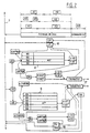
- Figure 1 shows a machine architecture with four modules.
- Figure 2 shows some details of the previously mentioned organ, located in a module considered local.
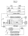
- FIG. 3 presents certain details of the previously mentioned member, located in a module considered distant.
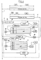
- Figure 4 shows other details of said member for implementing the invention.
- Figure 1 shows an example of machine architecture with non-uniform memory access consisting of four modules 10, 20, 40 and 60 interconnected by means of a ring 16.
- the description which follows with reference to figure 1 remains valid for any number of modules greater than or equal to two.
- the connection between the modules can be made using one or more switched rings or by any other type of connection such as interconnections in grids, hypercube or by auto switch (crossbar in English) for to name only a few of the best known.
- the interconnection of the modules allows make transactions between modules that use the memory consistency protocol.
- the module 10 includes four processors 1 to 4, a memory 5 and a connection member 6 to the other modules by the ring 16.
- the different elements 1 to 6 are interconnected by a system bus 7 in module 10.
- Module 20 includes four processors 21 to 24, one memory 25 and a member 26 for connection to the other modules by the ring 16.
- the different elements 21 to 26 are interconnected by a system bus 27 in the module 20.
- the module 40 comprises four processors 41 to 44, a memory 45 and a member 46 for connection to other modules by the ring 16.
- the various elements 41 to 46 are interconnected by a system bus 47 in module 40.
- Module 60 includes four processors 61 to 64, one memory 65 and a member 66 for connection to the other modules by the ring 16.
- the different elements 61 to 66 are connected together by a system bus 67 in the module 60.
- the member 6, respectively 26, 46, 66 is connected to the ring 16 by means of a link 17, respectively 37, 57, 77.
- Each processor 1 to 4, 21 to 24, 41 to 44, 61 to 64 respectively has a cache memory private, internal and or external, 11 to 14, 31 to 34, 51 to 54, 71 to 74.
- module 10 includes a remote access cache 15, named RC
- the module 20 includes a remote access cache 35, called RC
- the module 40 includes a cache 55 remote access, called RC
- the module 60 includes a cache memory 75 for access to distance, named RC. So that you can configure the size of cache 15, 35, 55 and or 75, it is advantageous to physically place it in a reserved area respectively from memory 5, 25, 45, 65, as shown in FIG. 1.
- Each processor 1 to 4, 21 to 24, 41 to 44 and 61 to 64 accesses blocks of contained data in memories 5 ', 25', 45 ', 65' using logical addresses from a single space addressing, without distinguishing whether the memories 5 ', 25', 45 ', 65' are local, belonging to the same module as the processor, or remote, belonging to a module other than the processor.
- module 10 it is organ 6 which distinguishes whether the logical address corresponds to a local physical block address residing in memory 5 ′, or if the logical address corresponds to a remote physical block address residing in one of the modules 20, 40, 60, for example by means of the most significant bits of the logical address which indicate the module where physically locates the addressed memory, the least significant bits then indicating the address physical inside the residency module.
- module 20 it is organ 26 which distinguishes if the logical address corresponds to a local physical block address residing in the 25 'memory, or if the logical address corresponds to a remote physical block address residing in one of the modules 40, 60, 10 for example by means of the most significant bits of the logical address which indicate the module where the addressed memory is physically located, the least significant bits then indicating the physical address inside the residence module, and so on for the other modules.
- the most significant bits previously mentioned constitute an A4 field of the logical address.
- the data blocks thus accessed constitute a set SM of memory shared by all the processors.
- processor 1 With reference to processor 1, remains valid for each of the others processors 2 to 4 with reference to module 10 as well as 21 to 24 with reference to module 20, 41 to 44 with reference to module 40 and 61 to 64 with reference to module 60.
- Processor 1 processes a word contained in a data block B1 of the set SM at using its private cache 11 according to a known cache mechanism, such as that with direct correspondence, with associative correspondence or associative by set of blocks, without it being necessary here to recall these different mechanisms.
- a cache essentially includes an access memory fast and a correspondence table not shown in the figures.
- a first field A1 called label
- a second field A2 called indexes
- a third field A3 called address of the word in the data block containing this word.
- the first and second fields constitute usually the logical address of block B1.
- Index A1 points to a line on a table of correspondence which basically contains two values.
- the first value is the label A1 'of a block B2 whose physical image is directly addressed in the access memory fast by this same index.
- the second value is a status code which indicates whether block B2 is owned exclusively by the processor, shared by another processor and in this case if its content is valid or if it has been modified by this other processor.
- block B2 If the label A1 of block B1 is equal to the label A1 'of block B2 and if the status code indicates exclusivity or valid content, block B2 is none other than block B1, content physically in the quick access memory and the processor can directly process the words contained in this block by physically addressing them in the quick access memory by means of the second and third fields of the logical address. If the status code indicates sharing, the cache mechanism sends a signal S1 on the bus 7 to indicate a modification to the address of block B1, so as to modify the status code of this block in the cache memories who share it.
- the processor cannot directly process words contained in this block by physically addressing them in the quick access memory to the by means of the second and third fields of the logical address.
- the cache mechanism sends a Q2 request to write block B2 to the shared memory to free a place in the cache at the physical address indicated by index A2 then sends a request Q1 to read block B1 in memory shared so as to load block B1 in the cache memory at the physical address indicated by index A2. Otherwise, the cache mechanism sends a Q1 request to read block B1. in the shared memory so as to load the block B1 in the cache memory at the address physical indicated by index A2.
- FIG. 2 presents a first level of details of the member 6, with the material elements and logic implemented when a block address consisting of fields A1 and A2, flows on bus 7 being linked to a signal S1, a request Q1 or Q2.
- Organ 6, named RCC includes a table 8, named LMD, a table 9, named RCT, a register 18 and a register 19.
- the block address is also divided into three fields A4 to A6 or two fields A7 and A8.
- the A4 field consists of the most significant bits than those of the A5 field and the field A6 is made up of the least significant bits than those of field A5.
- Field A8 is consists of the least significant bits and the field A7 consists of the most significant bits in quantity higher than that of the bits in the A4 field so as to cover the A4 field.
- the member 6 When the member 6 sees on the bus 7, the signal S1, the request Q1 or the request Q2, it processes the block concerned by a cache mechanism using its table 8 if the weight bits contained in the A4 field of the logical address indicate that the block concerned resides physically in memory 5 ′, local to module 10, and using its table 9 if the bits of high weight of the label indicate that the block concerned physically resides in one of the modules 20, 40 or 60 remote.
- Table 8 is indexed by m bits constituting a field A5 of the logical address succeeding the most significant bits of the label. The value of the number m directly determines the size of the table 8 whose number of rows is then equal to 2 m .
- Each line of table 8 contains the least significant bits constituting a field A6 of the logical address of a block shared with one or more remote modules and a status code S2.
- the status code S2 is for example a byte made up of presence bits and status bits.
- Each module 20, 40, 60, remote from module 10 in which the block referenced by fields A5 and A6 resides, is assigned a presence bit to indicate the presence or absence of sharing of this block with said remote module 20 , 40, 60.
- the line of table 8 indexed by the m bits of field A5, contains an address value A6 equal to that of the block processed and that at least one bit of the status code indicates a sharing, this means that a module other than module 10, for example module 20, has accessed it previously.
- the processing of the block then depends on its previous access by the module 20 remote and processing related to this block. If the S2 status code indicates that the block is currently in shared use, organ 6 determines whether it is necessary to make a transaction with the remote module 20.
- S2 status code indicates that the block has been modified by a remote module
- a Q1 request of reading requires a transaction with the remote module which holds a valid copy of the block to bring this valid copy back to the physical memory resident in module 10
- unit 6 then generates a local failure signal LM to indicate access to local memory missed (local miss in English) which are accompanied by at least one transaction with a module distant.
- the signal LM is written in the register 18, then the member 6 updates the code S2 to a status not changed at the end of the transaction.
- a Q1 read request does not require a transaction with any remote module because module 10 holds a valid copy of the block
- unit 6 then generates an LH signal of local success.
- a signal S1 of modification or a request Q2 to write the block requires a transaction with each remote module for which a bit of the S2 code indicates a presence, of so as to signal to him that the copy of the block he holds is not valid, unit 6 then generates a local failure signal LM.
- Table 9 is indexed by n least significant bits of the logical address which constitute a field A8. The value of the number n directly determines the size of the table 9 whose number of rows is then equal to 2 n .
- Each line of table 9 contains a status code S3 and field A7 of the logical address which references a block copy directly indexed in cache 15 by field A8. The size of cache 15 is therefore 2 n blocks.
- the status code S3 is for example made up of two bits to code three states Inv, Sha, Mod, which indicate the state of a block referenced in table 9 by the field A8.
- the state Inv indicates that the referenced block is invalid, that is to say that the referenced block has been modified by a remote module 20, 40 or 60.
- the Sha state indicates that the referenced block is shared by at least one module remote 20, 40, 60.
- the Mod state indicates that the referenced block has been modified by the local module 10 and that its copy in cache memory 15 is up to date.
- the block indexed by the n bits of field A8 contains a field value A7 'equal to that of the block processed, this means that the block resides in a module other than module 10, for example in module 20, has been copied in cache 15 common to processors 1 to 4.
- the size of the cache is dimensioned to contain 2 n blocks referenced in table 9.
- the size of table 9 being configurable by choice of the value of n, it is similarly, the size of cache memory 15.
- An interesting way of enabling this parametrability is to remove from memory 5 a reserved address area and to allocate it to cache memory 15. This means is then reported in each module. remote 20, 40, 60 to allocate a reserved addressing area in the memory 25, 45, 65 to a cache memory 35, 55, 75.
- the size of the cache memories 15, 35, 55, 75 being small compared to that of the memories 5, 25, 45, 65, this means only slightly decreases the size memory common to all modules.
- the member 6 then considers the status code S3 of the block referenced in table 9, that is to say of the block processed by the signal S1 or a request Q1, Q2. If the S3 status code indicates that the block is invalid, unit 6 generates the same transactions and the same signals as if the line indexed by the n bits of field A8 contains a field value A7 'different from that of processed block, as explained later in the description.
- the member 6 determines whether it is necessary to make a transaction with the remote module 20. For the signal S1, a transaction is necessary to write in the status code S2 of the module 20, in which the block is resident, that the block is modified, and in the module status code S3 40 or 60 which has a copy of the block in its cache 55, 75, that the block is invalid; member 6 then generates a remote failure signal RM to indicate a missed remote access (remote miss in English) for which at least one transaction with a remote module is triggered. Unit 6 declares in its status code S3 that the block is modified. For the Q2 write request to memory, remote to module 10, no transaction is necessary and the member 6 generates a remote HR success signal.
- the line indexed by the n bits contains an address value different from that of the block processed, this means that the block logically addressed in cache 15 by indexing the table 9, is different from the treated block. It is then necessary to replace the block referenced in the table 9 by the treated block.
- the member 6 then generates an RM signal.
- Organ 6 also generates in this case a signal S4 to indicate a replacement in the cache memory 15, of the block listed by the treated block.
- the signal S4 is sent on the bus 7 to invalidate, in the private caches 11 at 14, the block listed in cache 15 because table 9 can no longer ensure its consistency.
- Unit 6 also informs Unit 26, 46 or 66 of the residency module that it does not plus reference the block so that member 26, 46 or 66 lowers the presence bit corresponding to module 10 in the row of table 28, 48 or 68 where the block was referenced.
- the organ6 then performs an update of the table 9 by means of a transaction with the remote modules 20, 40 and 60 to bring the treated block back to an addressed physical location logically in cache 15 by indexing table 9.
- the transaction consists essentially to send a read request to the remote module 20, 40 or 60 block residence.
- the module block residence is module 20.
- Figure 3 shows a second level of detail of the member 6, 26, 46, 66, with the elements hardware and logic implemented when a block address consisting of fields A1 and A2, arrives in the residence module of this block, from other modules via the link 17, 37, 57, 77.
- the remarks made in the introductory preamble to Figure 2 remain valid for figure 3.
- the references put on figure 3 are those of the member 26 to facilitate the following description.
- the member 26 transmits a copy of the block to the member 6. This copy is obtained by reading in memory 25 or in one of the cache memories 31 to 34. If the status code indicates that the block is modified, the unit 26 sends a read request to that of the modules 40, 60 which has the most up-to-date version of the block. Organ 46, 66 which has the most up-to-date copy, transmits the copy of the block to organ 6 of module 10 and organ 26 of module 20. Organ 26 updates its local memory 25 ′, and its code S2 to shared status. Organ 6 lists the block in table 9 with a shared and unmodified status code and writes the block in cache 15. Then, organ 6 emits an acknowledgment to organ 26 which adds to its S2 status code shares it with module 10.
- the member 26 If the processed block is not listed in table 28, the member 26 generates a signal S5 for indicate that the block listed will be replaced by the treated block. If the S2 status code of the block listed indicates that it has been modified by a module 10, 40 or 60, the unit 26 emits a read request to that of modules 10, 40, 60 which has the most up-to-date version of the block.
- the member 6, 46, 66 whose code S3 of the block referenced indicates that its copy of the block is modified, transmits a copy of the block to unit 26 of module 20 to update its local memory 25 '.
- the signal S5 is sent to the organ or organs 6, 46, 66 which reference the block to a line of their table 9, 49, 69, so that everyone updates their S3 code to invalid status.
- the member 26 lists the block processed in its table 28 with a code of S2 status indicating that the block is shared with module 10, unmodified. Finally, organ 26 transmits the content of the processed block to organ 6 which lists the block in table 9 with a non invalidated, shared and unmodified status code and writes the block to cache 15. If the S2 status code of the block listed in table 28, does not indicate that it has been modified, signal S5 is sent to the organ or organs 6, 46, 66 which reference the block at a line of their table 9, 49, 69 so that everyone updates their S3 code to invalid status. Then, the member 26 lists the block processed in its table 28 with a status code S2 indicating that the block is shared with module 10, unmodified. Finally, the organ 26 transmits the content of the block processed towards organ 6 which lists the block in table 9 with a non-status code invalidated, shared and not modified and writes the block in cache 15.
- a line is available if no block is referenced there or if the code of S2 status of the block already referenced indicates no presence of sharing with a remote module, the reference of such a block then being said to be invalid.
- a line is available if less than four blocks are referenced there or if the reference of at least one block already referenced is invalid. Chances that the reference of an already referenced block will be invalid before a new one block to be referenced thus increased in comparison to a matching mechanism direct. If a replacement is necessary due to unavailability of the line, it may be done on the oldest block or on the block with the smallest number of presence bits raised in its S2 status code. This reduces the possibility that another module will ask again immediately reference a block that has just been replaced.
- Figure 4 shows additional details of the organ 6.
- the organs 26, 46, 66 are identical.
- the division of a block address circulating on the bus 7, is here represented only by the fields A7 and A8, the most significant bits of the field A7 comprising the field A4, and the splitting of a block address from link 17, is here only represented by fields A4 to A6, because we saw previously that fields A1 and A2 were more particularly useful for the level of private caches 11 to 14.
- a filter 85 directs a block address circulating on bus 7, to table 9 if field A4 concerns an address of block residing in a module 20, 40, 60, distant from module 10.
- An index register 94 points on an entry in table 9 addressed by field A8 of the block address.
- 82 needle filter a block address from link 17, to table 8 if field A4 concerns a block address residing in module 10.
- An index register 84 points to an entry in the table 8 addressed by field A5 of the block address.
- Filters 82 and 85 are separate or have all or part of their elements in common.
- a counter 83 is incremented.
- the counter 83 records the number of accesses to the table 8 by a remote module.
- the counter 83 can be read from the bus 7.
- the filter 82 directing the address of the block to table 8, we have seen about the description in FIG. 3 that the member 6 determined whether the block was already listed in table 8 in comparing field A6 of the incoming block with field A6 'of a block already listed in a row of table 8 If no row of table 8 pointed to by register 84 was available for contain a value A6 'equal to the value of field A6 of the address of the block presented, a signal S5 was generated in organ 6 to indicate the need for replacement, so that index the block requested from link 17 in place of a block previously listed. This replacement also generates one or more transactions with the other modules.
- a replacement counter 81 is incremented.
- the contents counter 81 is accessible on bus 7, for example in input-output type reading.
- the counter 93 records the number of accesses to the table 9 by the local module 10.
- the counter 93 is accessible in reading by the bus 7.
- each access to the table 9 by the module 10 generated an RH signal or an RM signal. If the number of RH signals and the number of RM signals are counted moreover, the number of accesses to table 9 can be calculated as being equal to the sum of the number of RH signals and number of RM signals.
- the filter 85 directs the address of the block to table 9, we have seen about the description of FIG. 2 that, if the value A7 ′ contained in the line of the table 8 pointed to by the register 84 was different from the value of field A7 of the address of the block presented, a signal S4 was generated in organ 6 to indicate the need for replacement, so as to list the block circulating on bus 7 in place of the block previously listed. This replacement also generates one or more transactions with the other modules 20, 40, 60, to store in memory 15, an updated copy of the newly listed block. Every signal generation S4, a replacement counter 91 is incremented. The content of counter 91 is accessible on bus 7, for example in input-output type reading.
- the content of counter 91 is correlated to the number of transactions necessary to make replacements in table 9, and only among these transactions.
- the content of counter 91 is independent of transactions which do not require no replacement. For example in Figure 2, if the status code S3 of the block contained in the line pointed by field A8 indicates an invalid state, at least one transaction is necessary with a remote module. However, if the value A7 'contained in this line is equal to the value of field A7, the addressed block is already listed and therefore does not require replacement of this line. Although generating an RM failure signal, this case does not influence the contents of counter 91.
- Each of the counters 81, 83, 91, 93 is provided to send an interruption on bus 7 overflow.
- a control register 86 and a status register 87 are provided to send an interruption on bus 7 overflow.
- the register 86 is accessible on the bus 7 for reading and writing.
- the register 87 is accessible on bus 7 for reading and systematically reset to zero by reading its content.
- Register 87 contains, for each counter 81, 83, 92, 93, a bit including a logic state determined signals an overflow of the counter to which this bit is assigned.
- Register 86 contains bits to control counters 81, 83 91, 93 by means of a combinational logic not shown so as not to overload the figure unnecessarily.
- a first bit is provided to unconditionally deactivate counters 81 and 83 so that a logical state of the bit means that the counter contents cannot be modified after all new access to table 8 and for the complementary logical state of the bit to cause the contents of counters can be modified following any new access to table 8.
- a second bit is provided for conditionally deactivating counters 81 and 83 so that a state bit logic means that the contents of counters cannot be modified by a new access to table 8, following an overflow signaled by a bit of register 87 and that the state additional logic of the bit means that the contents of counters 81 and 83 can be modified by a new access to table 8, independently of the content of register 87.
- a third bit is provided to deactivate the interruption in the event of an overflow mentioned previously, so that a logical state of the bit makes the interrupt active and the complementary logic state of the bit makes the interrupt inactive.
- a fourth bit is provided to reset the contents of counters 81, 83.
- a first, a second, a third and a fourth bit manage activation of counters 91 and 93.
- These bits can be the same as those managing the counters 81 and 83 or bits specific to counters 91 and 93.
- a fourth can be provided bit common to all counters or as many fourth bits as there are counters, each fourth bit then acting on the counter to which it is assigned.
- registers 86 and 87 allows the creation of different types of measurement process implemented by programs executed in processors 1 to 4. We can cite those triggered by an interrupt generated in register 87, or those triggered periodically by interacting with register 86.
- a measurement process reads simultaneously the content of the two counters 81, 83 and or of the two counters 91, 93 and processes the values obtained.
- the measurement process determines a replacement rate by accessing the remote modules 20, 40, 60 to table 8.
- the measurement process determines a replacement rate by access from the local module 10 to table 9.
- each replacement in table 8 or in table 9 was accompanied by one or more transactions between modules to update or invalidate copies of blocks held by modules other than the residence module. These transactions have latencies of which too much accumulation risks significantly slowing down the machine. he it is preferable to set a threshold for the number of replacements per access, the excess of which is deemed to adversely affect machine performance.
Landscapes
- Engineering & Computer Science (AREA)
- Theoretical Computer Science (AREA)
- Physics & Mathematics (AREA)
- General Engineering & Computer Science (AREA)
- General Physics & Mathematics (AREA)
- Memory System Of A Hierarchy Structure (AREA)
- Memory System (AREA)
- Multi Processors (AREA)
Abstract
Description
un module considéré comprenant une mémoire physique constituée d'au moins deux parties,
- une première partie pour contenir des blocs de données résidents dans le module considéré,
- une deuxième partie pour contenir des copies de bloc de données résidents dans d'autres modules,
- doter le module considéré de deux tables LMD et RCT contenant chacune un nombre de lignes prédéterminé, chaque ligne de la première table LMD étant destinée à répertorier une adresse de bloc résident dans la première partie de mémoire physique disponible pour être partagé avec un ou plusieurs autres modules et à répertorier une autre adresse de bloc résident dans la première partie de mémoire physique par remplacement suite à une demande d'accès par un autre module, chaque ligne de la deuxième table RCT étant destinée à référencer une adresse de bloc résident dans un autre module et dont une copie est accessible à un emplacement de la deuxième partie de mémoire physique correspondant à cette ligne et à référencer une autre adresse de bloc résident dans un autre module par remplacement suite à une demande d'accès par le module considéré,
- faire fonctionner la machine dans un mode d'exploitation donné, en comptant un nombre de remplacements dans la première table LMD et ou un nombre de remplacements dans la deuxième table RCT,
- adapter l'architecture de la machine de façon à ce que le nombre de remplacements dans la première ou dans la deuxième table soit en moyenne inférieur à un seuil pour ledit mode d'exploitation donné.
chaque module considéré comprenant une mémoire physique constituée d'au moins deux parties,
- une première partie pour contenir des blocs de données résidents dans le module considéré,
- une deuxième partie pour contenir des copies de bloc de données résidents dans d'autres modules,
- deux tables LMD et RCT contenant chacune un nombre de lignes prédéterminé, chaque ligne de la première table LMD étant destinée à répertorier une adresse de bloc résident dans la première partie de mémoire physique disponible pour être partagé avec un ou plusieurs autres modules et à répertorier une autre adresse de bloc résident dans la première partie de mémoire physique par remplacement suite à une demande d'accès par un autre module, chaque ligne de la deuxième table RCT étant destinée à référencer une adresse de bloc résident dans un autre module et dont une copie est accessible à un emplacement de la deuxième partie de mémoire physique correspondant à cette ligne et à référencer une autre adresse de bloc résident dans un autre module par remplacement suite à une demande d'accès par le module considéré,
- un compteur du nombre de remplacements dans la première table LMD et ou un compteur du nombre de remplacements dans la deuxième table RCT.
Claims (6)
- Procédé de production de machine constituée de plusieurs modules (10,20,40,60), un module (10) considéré comprenant une mémoire physique (5) constituée d'au moins deux parties,caractérisé en ce qu'il consiste à:une première partie (5') pour contenir des blocs de données résidents dans le module (10) considéré,une deuxième partie (15) pour contenir des copies de bloc de données résidents dans d'autres modules(20,40,60),doter le module (10) considéré de deux tables LMD et RCT contenant chacune un nombre de lignes prédéterminé, chaque ligne de la première table LMD (8) étant destinée à répertorier une adresse de bloc résident dans la première partie (5') de mémoire physique disponible pour être partagé avec un ou plusieurs autres modules (20,40,60) et à répertorier une autre adresse de bloc résident dans la première partie (5') de mémoire physique par remplacement suite à une demande d'un autre module (20,40,60), chaque ligne de la deuxième table RCT (9) étant destinée à référencer une adresse de bloc résident dans un autre module (20,40,60) et dont une copie est accessible à un emplacement de la deuxième partie (15) de mémoire physique correspondant à cette ligne et à référencer une autre adresse de bloc résident dans un autre module (20,40,60) par remplacement suite à une demande d'accès du module (10) considéré,faire fonctionner la machine dans un mode d'exploitation donné, en comptant un nombre de remplacements dans la première table LMD (8) et ou un nombre de remplacements dans la deuxième table RCT (9),adapter l'architecture de la machine de façon à ce que le nombre de remplacements dans la première ou dans la deuxième table soit en moyenne inférieur à un seuil pour ledit mode d'exploitation donné.
- Procédé selon la revendication 1, caractérisé en ce que l'architecture de la machine est adaptée en munissant la première (8) et ou la deuxième table (9) d'un nombre de lignes tel que le nombre de remplacements soit en moyenne inférieur au dit seuil.
- Procédé selon la revendication 1, caractérisé en ce que la moyenne du nombre de remplacements dans la première table LMD (8), respectivement dans la deuxième table RCT (9), est calculée en divisant le nombre de remplacement par un nombre total d'accès à la première table LMD (8), respectivement à la deuxième table RCT (9).
- Machine constituée de plusieurs modules (10,20,40,60), chaque module considéré (10) comprenant une mémoire physique (5) constituée d'au moins deux parties,caractérisé en ce que le module considéré comprend:une première partie (5') pour contenir des blocs de données résidents dans le module considéré,une deuxième partie (15) pour contenir des copies de bloc de données résidents dans d'autres modules,deux tables LMD et RCT contenant chacune un nombre de lignes prédéterminé, chaque ligne de la première table LMD (8) étant destinée à répertorier une adresse de bloc résident dans la première partie de mémoire physique (5') disponible pour être partagé avec un ou plusieurs autres modules (20,40,60) et à répertorier une autre adresse de bloc résident dans la première partie de mémoire physique par remplacement suite à une demande d'accès d'un autre module, chaque ligne de la deuxième table RCT (9) étant destinée à référencer une adresse de bloc résident dans un autre module (20,40,60) et dont une copie est accessible à un emplacement de la deuxième partie de mémoire physique (15) correspondant à cette ligne et à référencer une autre adresse de bloc résident dans un autre module par remplacement suite à une demande d'accès du module considéré,un compteur (81) du nombre de remplacements dans la première table LMD et ou un compteur (91) du nombre de remplacements dans la deuxième table RCT.
- Machine constituée de plusieurs modules (10,20,40,60), selon la revendication 4, caractérisée en ce que chaque module comprend respectivement un organe (6,26,46,66) pour communiquer avec les autres modules, et en ce que chaque organe comprend deux tables du type des dites tables (8,9) et deux compteurs du type des dits compteurs (81,91).
- Machine constituée de plusieurs modules (10,20,40,60), selon la revendication 5, caractérisée en ce qu'un organe (6) comprend un moyen de comptage (83) du nombre total d'accès à la première table LMD (8) et ou un moyen de comptage (93) du nombre total d'accès à la deuxième table RCT (9).
Applications Claiming Priority (2)
| Application Number | Priority Date | Filing Date | Title |
|---|---|---|---|
| FR9706388A FR2763714B1 (fr) | 1997-05-26 | 1997-05-26 | Compteurs de remplacement pour machine avec memoire a acces non uniforme |
| FR9706388 | 1997-05-26 |
Publications (2)
| Publication Number | Publication Date |
|---|---|
| EP0881579A1 true EP0881579A1 (fr) | 1998-12-02 |
| EP0881579B1 EP0881579B1 (fr) | 2002-07-31 |
Family
ID=9507221
Family Applications (1)
| Application Number | Title | Priority Date | Filing Date |
|---|---|---|---|
| EP98401148A Expired - Lifetime EP0881579B1 (fr) | 1997-05-26 | 1998-05-14 | Compteurs de remplacement pour machine avec mémoire à accès non uniforme. |
Country Status (5)
| Country | Link |
|---|---|
| US (1) | US6148378A (fr) |
| EP (1) | EP0881579B1 (fr) |
| JP (1) | JPH10334068A (fr) |
| DE (1) | DE69806855T2 (fr) |
| FR (1) | FR2763714B1 (fr) |
Cited By (3)
| Publication number | Priority date | Publication date | Assignee | Title |
|---|---|---|---|---|
| WO2001029674A1 (fr) * | 1999-10-15 | 2001-04-26 | Silicon Graphics, Inc. | Procede et systeme multiprocesseur d'acces a des donnees |
| EP1233342A1 (fr) * | 2001-02-15 | 2002-08-21 | Bull S.A. | Contrôleur de cohérence pour ensemble multiprocesseur, module et ensemble multiprocesseur à architecture multimodule intégrant un tel contrôleur |
| EP1027655B1 (fr) * | 1997-11-05 | 2004-03-10 | Unisys Corporation | Etat d'optimisation d'une memoire |
Families Citing this family (19)
| Publication number | Priority date | Publication date | Assignee | Title |
|---|---|---|---|---|
| US6785888B1 (en) * | 1997-08-29 | 2004-08-31 | International Business Machines Corporation | Memory allocator for a multiprocessor computer system |
| US6826651B2 (en) * | 1998-05-29 | 2004-11-30 | International Business Machines Corporation | State-based allocation and replacement for improved hit ratio in directory caches |
| US6237065B1 (en) * | 1999-05-14 | 2001-05-22 | Hewlett-Packard Company | Preemptive replacement strategy for a caching dynamic translator |
| US6754784B1 (en) * | 2000-02-01 | 2004-06-22 | Cirrus Logic, Inc. | Methods and circuits for securing encached information |
| US6763432B1 (en) * | 2000-06-09 | 2004-07-13 | International Business Machines Corporation | Cache memory system for selectively storing directory information for a higher level cache in portions of a lower level cache |
| US6760809B2 (en) * | 2001-06-21 | 2004-07-06 | International Business Machines Corporation | Non-uniform memory access (NUMA) data processing system having remote memory cache incorporated within system memory |
| US7103636B2 (en) * | 2002-05-28 | 2006-09-05 | Newisys, Inc. | Methods and apparatus for speculative probing of a remote cluster |
| US7181744B2 (en) * | 2002-10-24 | 2007-02-20 | International Business Machines Corporation | System and method for transferring data between virtual machines or other computer entities |
| US7296121B2 (en) * | 2002-11-04 | 2007-11-13 | Newisys, Inc. | Reducing probe traffic in multiprocessor systems |
| US7346744B1 (en) | 2002-11-04 | 2008-03-18 | Newisys, Inc. | Methods and apparatus for maintaining remote cluster state information |
| US7003633B2 (en) * | 2002-11-04 | 2006-02-21 | Newisys, Inc. | Methods and apparatus for managing probe requests |
| JP4012517B2 (ja) | 2003-04-29 | 2007-11-21 | インターナショナル・ビジネス・マシーンズ・コーポレーション | 仮想計算機環境におけるロックの管理 |
| US7251815B2 (en) * | 2003-04-29 | 2007-07-31 | International Business Machines Corporation | Multiple virtual machines sharing processor and work queue in memory having program/dispatch functions for assigning and accessing work items while the virtual machine was not idle |
| US7299468B2 (en) * | 2003-04-29 | 2007-11-20 | International Business Machines Corporation | Management of virtual machines to utilize shared resources |
| US7334089B2 (en) * | 2003-05-20 | 2008-02-19 | Newisys, Inc. | Methods and apparatus for providing cache state information |
| US7698397B2 (en) * | 2003-06-27 | 2010-04-13 | Microsoft Corporation | Method and framework for providing system performance information |
| US7337279B2 (en) * | 2003-06-27 | 2008-02-26 | Newisys, Inc. | Methods and apparatus for sending targeted probes |
| WO2014128967A1 (fr) * | 2013-02-25 | 2014-08-28 | 株式会社日立製作所 | Dispositif de commande de stockage et procédé de détection d'achèvement d'écriture de données |
| JP6881485B2 (ja) * | 2019-02-26 | 2021-06-02 | 日本電気株式会社 | メモリ配置装置、メモリ配置方法、及び、メモリ配置プログラム |
Citations (1)
| Publication number | Priority date | Publication date | Assignee | Title |
|---|---|---|---|---|
| JPH02181844A (ja) * | 1989-01-06 | 1990-07-16 | Matsushita Electric Ind Co Ltd | キャッシュメモリ管理方法 |
Family Cites Families (3)
| Publication number | Priority date | Publication date | Assignee | Title |
|---|---|---|---|---|
| US4068304A (en) * | 1973-01-02 | 1978-01-10 | International Business Machines Corporation | Storage hierarchy performance monitor |
| US5887146A (en) * | 1995-08-14 | 1999-03-23 | Data General Corporation | Symmetric multiprocessing computer with non-uniform memory access architecture |
| US6014690A (en) * | 1997-10-24 | 2000-01-11 | Digital Equipment Corporation | Employing multiple channels for deadlock avoidance in a cache coherency protocol |
-
1997
- 1997-05-26 FR FR9706388A patent/FR2763714B1/fr not_active Expired - Fee Related
-
1998
- 1998-05-14 EP EP98401148A patent/EP0881579B1/fr not_active Expired - Lifetime
- 1998-05-14 DE DE69806855T patent/DE69806855T2/de not_active Expired - Lifetime
- 1998-05-22 US US09/082,938 patent/US6148378A/en not_active Expired - Lifetime
- 1998-05-26 JP JP10144680A patent/JPH10334068A/ja active Pending
Patent Citations (1)
| Publication number | Priority date | Publication date | Assignee | Title |
|---|---|---|---|---|
| JPH02181844A (ja) * | 1989-01-06 | 1990-07-16 | Matsushita Electric Ind Co Ltd | キャッシュメモリ管理方法 |
Non-Patent Citations (4)
| Title |
|---|
| KUMAR M J ET AL: "HIERARCHICAL DIRECTORY-BASED SHARED MEMORY ARCHITECTURE", COMPUTER JOURNAL, vol. 38, no. 3, 1 January 1995 (1995-01-01), pages 207 - 216, XP000558437 * |
| LENOSKI D ET AL: "THE DASH PROTOTYPE: LOGIC OVERHEAD AND PERFORMANCE", IEEE TRANSACTIONS ON PARALLEL AND DISTRIBUTED SYSTEMS, vol. 4, no. 1, 1 January 1993 (1993-01-01), pages 41 - 61, XP000381324 * |
| PATENT ABSTRACTS OF JAPAN vol. 014, no. 462 (P - 1113) 5 October 1990 (1990-10-05) * |
| VERGHESE B ET AL: "OPERATING SYSTEM SUPPORT FOR IMPROVING DATA LOCALITY ON CC-NUMA COMPUTE SERVERS", ACM SIGPLAN NOTICES, vol. 31, no. 9, September 1996 (1996-09-01), pages 279 - 289, XP000639239 * |
Cited By (5)
| Publication number | Priority date | Publication date | Assignee | Title |
|---|---|---|---|---|
| EP1027655B1 (fr) * | 1997-11-05 | 2004-03-10 | Unisys Corporation | Etat d'optimisation d'une memoire |
| WO2001029674A1 (fr) * | 1999-10-15 | 2001-04-26 | Silicon Graphics, Inc. | Procede et systeme multiprocesseur d'acces a des donnees |
| US6651157B1 (en) | 1999-10-15 | 2003-11-18 | Silicon Graphics, Inc. | Multi-processor system and method of accessing data therein |
| EP1233342A1 (fr) * | 2001-02-15 | 2002-08-21 | Bull S.A. | Contrôleur de cohérence pour ensemble multiprocesseur, module et ensemble multiprocesseur à architecture multimodule intégrant un tel contrôleur |
| US7017011B2 (en) | 2001-02-15 | 2006-03-21 | Bull S.A. | Coherence controller for a multiprocessor system, module, and multiprocessor system with a multimodule architecture incorporating such a controller |
Also Published As
| Publication number | Publication date |
|---|---|
| FR2763714A1 (fr) | 1998-11-27 |
| JPH10334068A (ja) | 1998-12-18 |
| US6148378A (en) | 2000-11-14 |
| FR2763714B1 (fr) | 1999-07-02 |
| DE69806855D1 (de) | 2002-09-05 |
| DE69806855T2 (de) | 2003-02-06 |
| EP0881579B1 (fr) | 2002-07-31 |
Similar Documents
| Publication | Publication Date | Title |
|---|---|---|
| EP0881579B1 (fr) | Compteurs de remplacement pour machine avec mémoire à accès non uniforme. | |
| EP0881574B1 (fr) | Dispositif d'instrumentation pour machine avec mémoire à accès non uniforme. | |
| EP1233342B1 (fr) | Contrôleur de cohérence pour ensemble multiprocesseur, module et ensemble multiprocesseur à architecture multimodule intégrant un tel contrôleur | |
| EP0883064B1 (fr) | Détection de points chauds dans une machine avec mémoire à accès non uniforme. | |
| US10891228B2 (en) | Cache line states identifying memory cache | |
| US7318144B2 (en) | Apparatus and method for interconnecting a processor to co-processors using shared memory | |
| EP2864891B1 (fr) | Systeme et procede de traitement de donnees a gestion d'une coherence de caches dans un reseau de processeurs munis de memoires caches | |
| FR2834809A1 (fr) | Dispositif pour moteur de compression de memoire cache pour la compression de donnees sur des memoires cache integrees pour augmenter la taille de memoire cache effective | |
| CN104508637A (zh) | 用于对等缓存转发的方法 | |
| CN101189590A (zh) | 使用流寄存器过滤监听请求的方法和装置 | |
| CN105190574B (zh) | 在共享存储环境中提供本地高速缓存一致性 | |
| FR2927437A1 (fr) | Systeme informatique multiprocesseur | |
| WO2013156716A1 (fr) | Systeme et procede de gestion d'une coherence de caches dans un reseau de processeurs munis de memoires caches | |
| FR2737030A1 (fr) | Procede de transfert de messages dans un systeme informatique multinodal | |
| US12141066B2 (en) | Probe filter directory management | |
| EP0636988B1 (fr) | Procédé de gestion cohérente des échanges entre des niveaux d'une hiérarchie de mémoires à au moins trois niveaux | |
| CN104077238A (zh) | 运算处理设备、信息处理设备及控制信息处理设备的方法 | |
| FR2609195A1 (fr) | Procede de gestion d'antememoires associees a des processeurs dans une architecture multiprocesseur a bus unique et systeme de traitement de donnees fonctionnant suivant ce procede | |
| EP1049018A1 (fr) | Architecture d'interconnexion modulaire pour machine multiprocesseur extensible, mettant en oeuvre une hiérarchie de bus virtuelle à plusieurs niveaux et la même brique de base pour tous les niveaux | |
| US7149218B2 (en) | Cache line cut through of limited life data in a data processing system | |
| WO1995002865A1 (fr) | Procede de gestion de memoires d'un systeme informatique, systeme informatique et memoire mettant en ×uvre le procede | |
| US11947418B2 (en) | Remote access array | |
| US20240037038A1 (en) | Coherency Domain Cacheline State Tracking | |
| FR3022653A1 (fr) | Reduction des evictions dans les repertoires de gestion de memoire cache | |
| EP0822495A1 (fr) | Distribution de tickets dans un système informatique multinodal |
Legal Events
| Date | Code | Title | Description |
|---|---|---|---|
| PUAI | Public reference made under article 153(3) epc to a published international application that has entered the european phase |
Free format text: ORIGINAL CODE: 0009012 |
|
| AK | Designated contracting states |
Kind code of ref document: A1 Designated state(s): DE FR GB IT |
|
| AX | Request for extension of the european patent |
Free format text: AL;LT;LV;MK;RO;SI |
|
| 17P | Request for examination filed |
Effective date: 19990602 |
|
| AKX | Designation fees paid |
Free format text: DE FR GB IT |
|
| GRAG | Despatch of communication of intention to grant |
Free format text: ORIGINAL CODE: EPIDOS AGRA |
|
| 17Q | First examination report despatched |
Effective date: 20010607 |
|
| GRAG | Despatch of communication of intention to grant |
Free format text: ORIGINAL CODE: EPIDOS AGRA |
|
| GRAG | Despatch of communication of intention to grant |
Free format text: ORIGINAL CODE: EPIDOS AGRA |
|
| GRAH | Despatch of communication of intention to grant a patent |
Free format text: ORIGINAL CODE: EPIDOS IGRA |
|
| GRAH | Despatch of communication of intention to grant a patent |
Free format text: ORIGINAL CODE: EPIDOS IGRA |
|
| GRAA | (expected) grant |
Free format text: ORIGINAL CODE: 0009210 |
|
| AK | Designated contracting states |
Kind code of ref document: B1 Designated state(s): DE FR GB IT |
|
| REG | Reference to a national code |
Ref country code: GB Ref legal event code: FG4D Free format text: NOT ENGLISH |
|
| GBT | Gb: translation of ep patent filed (gb section 77(6)(a)/1977) |
Effective date: 20020731 |
|
| REF | Corresponds to: |
Ref document number: 69806855 Country of ref document: DE Date of ref document: 20020905 |
|
| PLBE | No opposition filed within time limit |
Free format text: ORIGINAL CODE: 0009261 |
|
| STAA | Information on the status of an ep patent application or granted ep patent |
Free format text: STATUS: NO OPPOSITION FILED WITHIN TIME LIMIT |
|
| 26N | No opposition filed |
Effective date: 20030506 |
|
| REG | Reference to a national code |
Ref country code: FR Ref legal event code: PLFP Year of fee payment: 18 |
|
| PGFP | Annual fee paid to national office [announced via postgrant information from national office to epo] |
Ref country code: DE Payment date: 20150623 Year of fee payment: 18 Ref country code: GB Payment date: 20150626 Year of fee payment: 18 |
|
| PGFP | Annual fee paid to national office [announced via postgrant information from national office to epo] |
Ref country code: FR Payment date: 20150625 Year of fee payment: 18 |
|
| PGFP | Annual fee paid to national office [announced via postgrant information from national office to epo] |
Ref country code: IT Payment date: 20150624 Year of fee payment: 18 |
|
| REG | Reference to a national code |
Ref country code: DE Ref legal event code: R119 Ref document number: 69806855 Country of ref document: DE |
|
| GBPC | Gb: european patent ceased through non-payment of renewal fee |
Effective date: 20160514 |
|
| PG25 | Lapsed in a contracting state [announced via postgrant information from national office to epo] |
Ref country code: IT Free format text: LAPSE BECAUSE OF NON-PAYMENT OF DUE FEES Effective date: 20160514 |
|
| REG | Reference to a national code |
Ref country code: FR Ref legal event code: ST Effective date: 20170131 |
|
| PG25 | Lapsed in a contracting state [announced via postgrant information from national office to epo] |
Ref country code: DE Free format text: LAPSE BECAUSE OF NON-PAYMENT OF DUE FEES Effective date: 20161201 Ref country code: FR Free format text: LAPSE BECAUSE OF NON-PAYMENT OF DUE FEES Effective date: 20160531 |
|
| PG25 | Lapsed in a contracting state [announced via postgrant information from national office to epo] |
Ref country code: GB Free format text: LAPSE BECAUSE OF NON-PAYMENT OF DUE FEES Effective date: 20160514 |