EP0881693A1 - Referenzspannung in einer integrierten Schaltung - Google Patents
Referenzspannung in einer integrierten Schaltung Download PDFInfo
- Publication number
- EP0881693A1 EP0881693A1 EP98410059A EP98410059A EP0881693A1 EP 0881693 A1 EP0881693 A1 EP 0881693A1 EP 98410059 A EP98410059 A EP 98410059A EP 98410059 A EP98410059 A EP 98410059A EP 0881693 A1 EP0881693 A1 EP 0881693A1
- Authority
- EP
- European Patent Office
- Prior art keywords
- voltage
- integrated circuit
- type
- region
- transistor
- Prior art date
- Legal status (The legal status is an assumption and is not a legal conclusion. Google has not performed a legal analysis and makes no representation as to the accuracy of the status listed.)
- Withdrawn
Links
- 238000001465 metallisation Methods 0.000 description 4
- 239000006185 dispersion Substances 0.000 description 3
- 239000000758 substrate Substances 0.000 description 3
- 238000009792 diffusion process Methods 0.000 description 2
- 238000002955 isolation Methods 0.000 description 2
- 230000001681 protective effect Effects 0.000 description 2
- XUIMIQQOPSSXEZ-UHFFFAOYSA-N Silicon Chemical compound [Si] XUIMIQQOPSSXEZ-UHFFFAOYSA-N 0.000 description 1
- 238000010586 diagram Methods 0.000 description 1
- 229910052710 silicon Inorganic materials 0.000 description 1
- 239000010703 silicon Substances 0.000 description 1
- 230000006641 stabilisation Effects 0.000 description 1
- 238000011105 stabilization Methods 0.000 description 1
Images

Classifications
-
- H—ELECTRICITY
- H10—SEMICONDUCTOR DEVICES; ELECTRIC SOLID-STATE DEVICES NOT OTHERWISE PROVIDED FOR
- H10D—INORGANIC ELECTRIC SEMICONDUCTOR DEVICES
- H10D8/00—Diodes
- H10D8/20—Breakdown diodes, e.g. avalanche diodes
- H10D8/25—Zener diodes
-
- G—PHYSICS
- G05—CONTROLLING; REGULATING
- G05F—SYSTEMS FOR REGULATING ELECTRIC OR MAGNETIC VARIABLES
- G05F3/00—Non-retroactive systems for regulating electric variables by using an uncontrolled element, or an uncontrolled combination of elements, such element or such combination having self-regulating properties
- G05F3/02—Regulating voltage or current
- G05F3/08—Regulating voltage or current wherein the variable is DC
- G05F3/10—Regulating voltage or current wherein the variable is DC using uncontrolled devices with non-linear characteristics
- G05F3/16—Regulating voltage or current wherein the variable is DC using uncontrolled devices with non-linear characteristics being semiconductor devices
Definitions
- the present invention relates to the field of circuits integrated and more particularly the training of a reference voltage in an integrated circuit.
- a voltage reference is a device that presents a substantially constant voltage across its terminals when it is traversed by a current within a certain value range.
- a characteristic sought for a reference of voltage is first of all that the voltage across it also remains constant as possible when the current flowing through the source of voltage varies within a relatively large range.
- a first classic type of voltage reference is a forbidden band type voltage reference (BAND GAP) which constitutes a particularly high tension reference precise and stable but which uses a large number of components and which therefore occupies a non-negligible integrated circuit surface.
- BAND GAP forbidden band type voltage reference
- Such voltage sources are not suitable in particular to constitute protective devices for limit the voltage between two terminals to a specific voltage of a device to be protected, for example between grid and source of a MOS transistor.
- Zener diode Zener Another known voltage reference is the diode Zener.
- This voltage reference has the advantage of being relatively simple to realize in an integrated circuit and occupy a small area.
- a Zener diode can simply be used as a voltage source or as a protective device at a given voltage.
- this device has the disadvantage of being unstable over time, that is to say that if a nominal current is circulated in a Zener diode for a long time, the voltage across its terminals drifts.
- the nominal voltage variation is commonly of the order of 0.06 volts per hour and can reach a value of the order of the volt after 1000 hours of use.
- an integrated circuit Zener diode has a constant voltage only on a low current range.
- an object of the present invention is to provide a voltage reference achievable in an integrated circuit and presenting the simplicity of a Zener diode and its low occupancy surface but whose tension is constant over a range larger current.
- Another object of the present invention is to provide a voltage reference which is stable over time.
- Another object of the present invention is to provide a voltage reference which can be carried out as simply in a bipolar integrated circuit than in an integrated circuit of MOS type.
- the present invention provides a voltage reference in an integrated circuit, consisting an NPN bipolar transistor whose base is not connected and whose transmitter corresponds to an anode and the collector to a cathode.
- the transistor is an NPN bipolar transistor of a circuit integrated bipolar type.
- the NPN bipolar transistor is formed in an N well of a MOS type integrated circuit, the transmitter corresponding to a drain-source region of an N-channel MOS transistor formed in a region corresponding to a drain-source region of a P-channel MOS transistor.
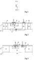
- the present invention provides for using a transistor in dipole bipolar NPN type connected between its collector and its transmitter, its base not being connected (being kept floating).
- the emitter terminal E corresponds to the anode terminal (+) and the collector terminal C corresponds to the cathode terminal (-) of the dipole. It will be shown below that such a device can be used in the same way as a Zener diode but present the advantage of better stability over time and more low voltage dispersion over a wide current range.
- FIG. 2 shows a first embodiment of the present invention.
- This figure represents a conventional NPN bipolar transistor formed in a bipolar integrated circuit.
- the bipolar transistor corresponds to a conventional technology in which a lightly doped N-type epitaxial layer 1 is formed on a P-type silicon substrate 2.
- a buried layer 3 is formed, before the growth of the layer epitaxial.
- the bipolar transistor comprises a P-type base region 5 formed in the epitaxial layer, an N-type emitter region 6 formed in the base region 5 and, an N + type region 7 serving as a collector contact.
- this region extends into a collecting well to come into contact with the buried layer 3.
- the component is surrounded by an isolation wall 8 of type P which crosses the epitaxial layer 1 .
- this device is used as voltage reference dipole, that is to say only provides for metallization of emitter E over the region of emitter 6 and metallization of collector C on the region of collector contact 7.
- FIG. 3 represents an embodiment of the present invention produced in an integrated circuit of the CMOS type, that is to say an integrated circuit in which provision is made to essentially form N-channel MOS transistors and MOS-channel transistors P.
- CMOS type complementary metal-oxide-semiconductor
- FIG. 3 a die in which an epitaxial layer 11 of type P is formed on a substrate 12 of type P + .
- N-channel MOS transistors are formed directly in the epitaxial layer 11 and P-channel MOS transistors are formed in N-type boxes formed in this epitaxial layer.
- Reference 13 indicates an example of such a box in which a component according to the present invention is made. This component comprises a P-type region 15 formed in the box 13.
- This P-type region corresponds for example to the implantation-diffusion of drains and sources of P-channel transistors.
- region 15 is formed an N-type region 16
- This region 16 corresponds for example to the implantation-diffusion of drains and sources of the N-channel MOS transistors.
- a collector contact resumption region 17 is formed at the same time as the region 16. A transistor is therefore obtained.
- NPN whose emitter corresponds to region 16, the base to region 15 and the collector to region 17. According to the invention, only one metallization of emitter E and one metallization of collector C. The resulting NPN transistor is formed will of course have a small gain since the region 15 is relatively heavily doped but is perfectly suitable for forming a voltage reference according to the invention.
- FIGS. 4 and 5 represent the characteristic of such a dipole in the particular case of FIG. 2.
- FIGS. 4 and 5 represent the same curve, the difference being that in Figure 4 the current is plotted in logarithmic coordinates and that in Figure 5 the current is plotted in linear coordinates.
- the voltage V T increases substantially regularly with the current until reaching a threshold value, equal to 4.74 volts in the example shown, as long as the current remains less than 1 microampere. Then, the voltage between terminals E and C remains substantially constant while the current increases from a value of the order of 1 ⁇ A to a value of the order of 10 mA. More particularly, a voltage of 4.80 volts for 11.6 mA was measured. Finally, for higher current values, the voltage varies as a function of the impedance of the circuit in which the component according to the invention is inserted.
- the invention works also when the epitaxial layer 11 is formed on a substrate type N. It also works whether or not a buried layer and, as previously indicated that we whether or not a collector well is provided.
- the advantage of forecasting collector well and the buried layer is that one increases the dynamic operating range.
- Figure 4 also shows for comparison the characteristic of an equivalent Zener diode consisting of a region of a first type of conductivity formed in the region of conductivity type opposite to the surface of an integrated circuit.
- the stabilization area of the diode Zener is less than three decades (from 1 ⁇ m to less than 1 mA) and that in this area the voltage varies by about 0.25 V.
- the voltage dispersion is therefore of the order of 5%, i.e. significantly larger than with the invention and on a smaller beach.
- Figure 6 represents the variation of voltage as a function of time.
- this variation is very small, for example on a duration of 5000 seconds, for a nominal voltage of the order of 5 volts, a variation in voltage was observed lower than the accuracy of the measuring device which was 5 mV while, with a Zener diode, the VZ characteristic presents a variation of substantially 50 mV after 5000 seconds of operation.
- the operation of the Zener diode is continued for for example a thousand hours, we observe a voltage variation of the order of a volt.
- the device according to the present invention achieves the objects sought to provide a source of tension stable over a wide current range and provide voltage stable over time.
- the temperature stability is at least equal to that of a Zener diode (of the order of + 1 mV / ° C).
- the present invention is particularly suitable for the creation of voltage references in circuits integrated very small dimensions, for example submicron.
Landscapes
- Physics & Mathematics (AREA)
- Engineering & Computer Science (AREA)
- Nonlinear Science (AREA)
- Electromagnetism (AREA)
- General Physics & Mathematics (AREA)
- Radar, Positioning & Navigation (AREA)
- Automation & Control Theory (AREA)
- Semiconductor Integrated Circuits (AREA)
- Metal-Oxide And Bipolar Metal-Oxide Semiconductor Integrated Circuits (AREA)
- Bipolar Integrated Circuits (AREA)
- Bipolar Transistors (AREA)
Applications Claiming Priority (2)
| Application Number | Priority Date | Filing Date | Title |
|---|---|---|---|
| FR9706907 | 1997-05-30 | ||
| FR9706907A FR2764138A1 (fr) | 1997-05-30 | 1997-05-30 | Reference de tension dans un circuit integre |
Publications (1)
| Publication Number | Publication Date |
|---|---|
| EP0881693A1 true EP0881693A1 (de) | 1998-12-02 |
Family
ID=9507599
Family Applications (1)
| Application Number | Title | Priority Date | Filing Date |
|---|---|---|---|
| EP98410059A Withdrawn EP0881693A1 (de) | 1997-05-30 | 1998-05-25 | Referenzspannung in einer integrierten Schaltung |
Country Status (3)
| Country | Link |
|---|---|
| EP (1) | EP0881693A1 (de) |
| JP (1) | JPH10335475A (de) |
| FR (1) | FR2764138A1 (de) |
Cited By (2)
| Publication number | Priority date | Publication date | Assignee | Title |
|---|---|---|---|---|
| FR2803143A1 (fr) * | 1999-12-28 | 2001-06-29 | St Microelectronics Sa | Dispositif ecreteur a resistance negative |
| EP1742272A1 (de) * | 2005-07-08 | 2007-01-10 | STMicroelectronics S.r.l. | Leistungsbauelement mit monolithischer Cascode-Struktur und integrierter Zener-Diode |
Citations (4)
| Publication number | Priority date | Publication date | Assignee | Title |
|---|---|---|---|---|
| US4170818A (en) * | 1975-06-16 | 1979-10-16 | Hewlett-Packard Company | Barrier height voltage reference |
| US4224631A (en) * | 1978-10-25 | 1980-09-23 | Raytheon Company | Semiconductor voltage reference device |
| US4870467A (en) * | 1985-08-06 | 1989-09-26 | Motorola, Inc. | Monolithic temperature compensated voltage-reference diode and method of its manufacture |
| US4886762A (en) * | 1985-08-06 | 1989-12-12 | Motorola Inc. | Monolithic temperature compensated voltage-reference diode and method for its manufacture |
-
1997
- 1997-05-30 FR FR9706907A patent/FR2764138A1/fr active Pending
-
1998
- 1998-05-21 JP JP10155420A patent/JPH10335475A/ja active Pending
- 1998-05-25 EP EP98410059A patent/EP0881693A1/de not_active Withdrawn
Patent Citations (4)
| Publication number | Priority date | Publication date | Assignee | Title |
|---|---|---|---|---|
| US4170818A (en) * | 1975-06-16 | 1979-10-16 | Hewlett-Packard Company | Barrier height voltage reference |
| US4224631A (en) * | 1978-10-25 | 1980-09-23 | Raytheon Company | Semiconductor voltage reference device |
| US4870467A (en) * | 1985-08-06 | 1989-09-26 | Motorola, Inc. | Monolithic temperature compensated voltage-reference diode and method of its manufacture |
| US4886762A (en) * | 1985-08-06 | 1989-12-12 | Motorola Inc. | Monolithic temperature compensated voltage-reference diode and method for its manufacture |
Cited By (4)
| Publication number | Priority date | Publication date | Assignee | Title |
|---|---|---|---|---|
| FR2803143A1 (fr) * | 1999-12-28 | 2001-06-29 | St Microelectronics Sa | Dispositif ecreteur a resistance negative |
| EP1132972A1 (de) * | 1999-12-28 | 2001-09-12 | STMicroelectronics S.A. | Begrenzungsanordnung mit negativem Widerstand |
| US6791808B2 (en) | 1999-12-28 | 2004-09-14 | Stmicroelectronics S.A. | Clipping device with a negative resistance |
| EP1742272A1 (de) * | 2005-07-08 | 2007-01-10 | STMicroelectronics S.r.l. | Leistungsbauelement mit monolithischer Cascode-Struktur und integrierter Zener-Diode |
Also Published As
| Publication number | Publication date |
|---|---|
| FR2764138A1 (fr) | 1998-12-04 |
| JPH10335475A (ja) | 1998-12-18 |
Similar Documents
| Publication | Publication Date | Title |
|---|---|---|
| EP0714139B1 (de) | Zweipoliges Bauteil zur Überkopfzündung mit kontrollierter Empfindlichkeit | |
| EP0357528B1 (de) | MOS-Transistor und Anwendung bei einer Freilaufdiode | |
| EP0040125B1 (de) | Schutzvorrichtung gegen Leckströme in integrierten Schaltungen | |
| FR2558010A1 (fr) | Procede pour la fabrication de transistors mos complementaires a basses tensions de seuil dans des circuits integres a haute densite et structure resultant de ce procede | |
| EP0432058B1 (de) | Dynamische Isolierschaltung für integrierte Schaltungen | |
| EP0543742A1 (de) | Monolithische Niederspannungsschutzdiode mit geringer Kapazität | |
| EP0614232B1 (de) | Referenzdiode in integriertem Bipolarschaltkreis | |
| FR3033938A1 (fr) | Diode zener a tension de claquage ajustable | |
| EP0543745B1 (de) | MOS-Transistor mit integrierter Zener-Schutzdiode | |
| EP0872891B1 (de) | Bauteil zum Schnittstellenschutz von Telefonleitungen | |
| EP0581625A1 (de) | Multifunktionale elektronische Vorrichtung, insbesondere Element mit dynamischem, negativem Widerstandsverhalten und Zugehöriges Herstellungsverfahren | |
| FR2507819A1 (fr) | Dispositif de protection contre les surcharges pour circuit integre et circuit integre de protection contre les surcharges | |
| FR2636481A1 (fr) | Diode active integrable | |
| EP0624943B1 (de) | Seriengeschaltetes Strombegrenzerbauelement | |
| FR2742933A1 (fr) | Composant statique et monolithique limiteur de courant et disjoncteur | |
| EP1748493A1 (de) | Speicherzelle mit einem Tranistor mit einem isolierten Körper und verbesserter Leseempfindlichkeit | |
| EP3276662A1 (de) | Struktur zum schutz eines integrierten schaltkreises gegen elektrostatische entladungen | |
| FR2764138A1 (fr) | Reference de tension dans un circuit integre | |
| CH651160A5 (fr) | Amplificateur differentiel a transistors bipolaires realises en technologie cmos. | |
| EP4297090A1 (de) | Mikroelektronische anordnung mit zwei feldeffekttransistoren | |
| FR2596202A1 (fr) | Structure de transistor npn equivalent a tension de claquage plus elevee que la tension de claquage intrinseque des transistors npn | |
| FR2708145A1 (fr) | Composant monolithique comprenant une diode de protection en parallèle avec une pluralité de paires de diodes en série. | |
| CA1245372A (fr) | Dispositif semiconducteur bipolaire et circuit mos incorporant un tel dispositif | |
| EP0562980A1 (de) | Selbsttätig geschützter Spannungsteiler | |
| EP2463632B1 (de) | Erfassungsvorrichtung, die einen robusten Testkreislauf umfasst |
Legal Events
| Date | Code | Title | Description |
|---|---|---|---|
| PUAI | Public reference made under article 153(3) epc to a published international application that has entered the european phase |
Free format text: ORIGINAL CODE: 0009012 |
|
| AK | Designated contracting states |
Kind code of ref document: A1 Designated state(s): AT BE CH CY DE DK ES FI FR GB GR IE IT LI LU MC NL PT SE |
|
| AX | Request for extension of the european patent |
Free format text: AL;LT;LV;MK;RO;SI |
|
| RAP3 | Party data changed (applicant data changed or rights of an application transferred) |
Owner name: STMICROELECTRONICS S.A. |
|
| AKX | Designation fees paid | ||
| STAA | Information on the status of an ep patent application or granted ep patent |
Free format text: STATUS: THE APPLICATION IS DEEMED TO BE WITHDRAWN |
|
| 18D | Application deemed to be withdrawn |
Effective date: 19990603 |