EP0881776A2 - Convertisseur analogique-numérique reconfigurable - Google Patents
Convertisseur analogique-numérique reconfigurable Download PDFInfo
- Publication number
- EP0881776A2 EP0881776A2 EP98303942A EP98303942A EP0881776A2 EP 0881776 A2 EP0881776 A2 EP 0881776A2 EP 98303942 A EP98303942 A EP 98303942A EP 98303942 A EP98303942 A EP 98303942A EP 0881776 A2 EP0881776 A2 EP 0881776A2
- Authority
- EP
- European Patent Office
- Prior art keywords
- converter
- bit
- digital signal
- output
- bit digital
- Prior art date
- Legal status (The legal status is an assumption and is not a legal conclusion. Google has not performed a legal analysis and makes no representation as to the accuracy of the status listed.)
- Withdrawn
Links
Images


Classifications
-
- H—ELECTRICITY
- H03—ELECTRONIC CIRCUITRY
- H03M—CODING; DECODING; CODE CONVERSION IN GENERAL
- H03M1/00—Analogue/digital conversion; Digital/analogue conversion
- H03M1/004—Reconfigurable analogue/digital or digital/analogue converters
- H03M1/007—Reconfigurable analogue/digital or digital/analogue converters among different resolutions
-
- H—ELECTRICITY
- H03—ELECTRONIC CIRCUITRY
- H03M—CODING; DECODING; CODE CONVERSION IN GENERAL
- H03M1/00—Analogue/digital conversion; Digital/analogue conversion
- H03M1/12—Analogue/digital converters
- H03M1/20—Increasing resolution using an n bit system to obtain n + m bits
- H03M1/202—Increasing resolution using an n bit system to obtain n + m bits by interpolation
- H03M1/206—Increasing resolution using an n bit system to obtain n + m bits by interpolation using a logic interpolation circuit
-
- H—ELECTRICITY
- H03—ELECTRONIC CIRCUITRY
- H03M—CODING; DECODING; CODE CONVERSION IN GENERAL
- H03M1/00—Analogue/digital conversion; Digital/analogue conversion
- H03M1/12—Analogue/digital converters
- H03M1/34—Analogue value compared with reference values
- H03M1/36—Analogue value compared with reference values simultaneously only, i.e. parallel type
- H03M1/361—Analogue value compared with reference values simultaneously only, i.e. parallel type having a separate comparator and reference value for each quantisation level, i.e. full flash converter type
- H03M1/362—Analogue value compared with reference values simultaneously only, i.e. parallel type having a separate comparator and reference value for each quantisation level, i.e. full flash converter type the reference values being generated by a resistive voltage divider
- H03M1/365—Analogue value compared with reference values simultaneously only, i.e. parallel type having a separate comparator and reference value for each quantisation level, i.e. full flash converter type the reference values being generated by a resistive voltage divider the voltage divider being a single resistor string
Definitions
- the present invention relates generally to an analog-to-digital (A/D)converter, and more particularly to an A/D converter that is selectively switchable (or "reconfigurable") between two resolution levels.
- a reconfigurable A/D converter of this type is particularly beneficial in a front-end signal-processing Integrated Circuit (IC), sometimes referred to as a Read Channel IC, that is used for reading data and servo signals from a computer hard-disk drive.
- IC Integrated Circuit
- A/D converters in general, operate according to a particular set of specifications. The most important of these are the resolution (number of bits) and the sampling frequency. For example, an 8 bit, 400 MHz A/D converter has a resolution of 8 bits and can produce 400 Million digital outputs in one second.
- Flash architecture is one well known method of implementing a high speed A/D converter. An example of flash architecture is disclosed in an article entitled "A 400 MHz input flash converter with error correction", IEEE Journal of Solid State Circuits , Vol. 25, No. 1, pp. 184-191, Feb. 1990 (C. Mangelsdorf). Flash architecture requires 2 N comparators for N bit resolution. Thus, a major drawback of flash architecture is that the size of the converter essentially doubles if the resolution is increased by one bit. As a consequence the power dissipation also roughly doubles, making it almost impractical to use this architecture for more than 10-bits of resolution.
- this architecture consumes less space than a standard flash A/D converter (a one-step A/D converter), it suffers from reduced speed since two passes, one after the other, are required to obtain the final conversion.
- Each of the two stages has the same resolution, and the final A/D output is derived by cascading the outputs of the two stages. For example, if the first stage has 4-bit resolution the second stage will also have 4-bit resolution, with the final word being given by concatenation of the two words in the same order.
- this could use this as a reconfigurable A/D converter by using only the first four bits in certain situations and all eight bits in other situations, but it would be very inefficient because the second pass would still need to be made, even though the information from the pass would be unused.
- this two-stage architecture can be pipelined so that the speed of conversion is the same as the conversion time of one stage, and the number of stages can be extended to be more than two.
- Such multi-step A/D converters are called pipelined multi-step A/D converters, an example of which is shown in an article entitled "A Pipelined 5 MHz Sample/9-bit Analog-to-Digital Converter", IEEE Journal of Solid State Circuits , Vol. SC-22, No. 6, pp. 954-961, Dec. 1987 (Stephen H. Levis and Paul R. Gray).
- the conversion rate is improved in these converters because of the pipelining, there is latency through the A/D converter that is equal to the sum of the delay through all of the stages.
- Magnetic mass storage devices such as disk drives, are used to store large amounts of data, especially in computer systems.
- Disk drives include a plurality of magnetized disks and a spindle motor to rotate the disks. Data is stored on concentric data tracks on the surfaces of the magnetized rotating disks.
- a sensor (usually referred to as a read/write head) positioned proximate the rotating disk and moveable in a radial direction is used to detect (i.e., read) information, in the form of analog signals, from the disks.
- a servo mechanism is used to determine and control the exact position of the read/write head with respect to the disk, so that data can be read from or written onto a specific sector and track on a specific disk.
- the first type is user data and this data is read during a user mode.
- the second type is servo data which is the data used by the servo mechanism to determine the position of the read/write head with respect to a specific sector on a specific track of the disk.
- the servo data is read in a servo mode.
- the electronics that are used for these two read modes vary widely from one manufacturer to another since there are no standards as to how these two processes should be implemented.
- an analog signal detected by the read head is first input into a very low-noise pre-amplifier which amplifies the signal.
- the amplified signal is then input into a read channel circuit.
- the read channel circuit is typically a single integrated circuit (IC) which directs the amplified signal to either the read path which processes the user data, or the servo path which processes servo data.
- the front end of the read channel consisting of a voltage gain amplifier (VGA) and a continuous-time filter (CTF), is common to both the servo and read signal processing.
- VGA voltage gain amplifier
- CTF continuous-time filter
- the processing circuitry for the user data is self-contained within the read channel IC (mostly analog). However, only part of the servo processing is done within the read channel IC. The majority of the servo processing, such as DSP operations and voice coil motor driving, is performed by separate circuits using one or more ICs. Essential to the servo processing is an A/D converter for digitizing the analog servo signals. In some disk-drive electronics, this A/D converter is part of the read channel IC, and in others it is embedded in a different chip.
- A/D converters are utilized in the user data circuit.
- the servo signal processing despite sharing most of the analog signal pre-processing with the user data path, continues to use a different A/D converter (either internal or external to the read channel IC) because in processing user data, high speed is more important than high resolution.
- high resolution is more important than high speed.
- the additional circuitry needed to process both types of data results in increased cost for such systems.
- the current invention pertains to merging these two A/D converters into a single reconfigurable A/D converter with minimal increase in size and cost.
- an A/D converter for sampling an input signal, the A/D converter having an output and further comprising reference means for generating a plurality of reference signals; comparing means for comparing the input signal with the reference signals and producing a set of digital signals corresponding to the difference between the input signal and the reference signals; multiplexer means for receiving the set of digital signals and outputting a first subset of the digital signals during a first predetermined time period and for outputting a second subset of the set of digital signals during a second predetermined time period; encoding means for encoding the.
- the first level of resolution (N) equals six (6) and the increase in resolution (R) equals one (1).
- fast mode is used to indicate the higher speed/low resolution (N-bit) operating mode and the term “slow mode” is used to indicate the lower speed/high resolution (N+R) operating mode.
- the present invention relates to an A/D converter that is capable of being shared both in the user mode and in the servo mode in connection with the control and processing circuitry of disk drives. This increases the amount of shared circuitry between the two processes and decreases the cost in implementing these two processes.
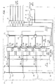
- a reconfigurable A/D converter in accordance with the present invention is generally indicated at 10.
- the reconfigurable A/D converter has two operating states. In first operating state the A/D converter generates an N-bit digital output signal in response to an analog input signal and in the second operating state the A/D converter 19 generates an (N + R) bit digital output signal in response to a second analog input signal (usually having a different data rate than the first analog signal).
- N indicates the lowest resolution or bit length of the A/D converter's digital output and is usually an integer.
- a set of reference voltages is generated by a reference circuit means.
- the reference circuit means is a resistor ladder 12 comprising a plurality of resistors 14a-14c (preferably a plurality of resistors having the same or substantially similar resistance values).
- the A/D converter includes 2 N comparators referred to generally by reference numeral 19, where N is the resolution as described above.
- Three comparators 19 (19a, 19b, and 19c) are shown in Fig. 1.
- a detailed view of one of the comparators 19 is shown in Fig. 1A.
- Each comparator 19 preferably has one voltage input V in , one reference input V ref , and two outputs Q and Q B .
- Each comparator 19 includes a differential amplifier 20 and a latch 22. The outputs of each differential amplifier 20 are input to their associated latch 22 as shown.
- the value of the reference voltage V ref being input to each comparator 19 will vary dependent upon the number of resistors 14 and the voltage V R applied to the top of the resistor ladder 12.
- the output of adjoining differential amplifiers 20 are also input to a second set of latches 13 (latches 13a, 13b and 13c are shown in Fig. 1), hereafter referred to as the interpolating latches.
- the interpolating latches 13 are similar to the latches 22 used in the comparator 19. There are generally 2 N interpolating latches 13.
- a mode control circuit 16 that is responsive to an external command bit/word, is part of the timing and control section of the A/D converter.
- the command bit/word may be generated by a logic circuit external to the A/D converter, e.g., a microprocessor.
- each differential amplifier 20 amplifies the voltage difference between its input voltage V in and its reference voltage V ref . If the input voltage V in is greater than the reference voltage V ref , then the output V OP of the differential amplifier 20 will be more positive than the output V ON of the same differential amplifier and vice versa.
- the difference between V OP and V ON of the differential amplifier, referred to as the differential output, is proportional to the difference between its two input signals V ref and V in (differential input), and the ratio of the output voltage difference to the input voltage difference is the voltage gain of the differential amplifier. Thus, the larger the input voltage difference, the larger the output voltage difference.
- each comparator 19 is having only two inputs (one input being V in and the other input being the reference voltage, V ref ), practical implementations may take on several forms.
- a fully differential comparator would have two complementary input voltages V inP and V inN , and two complementary reference voltages, V refP and V refN .
- a differencing circuit 77 precedes the comparator 19, and one input to 19 receives V inP - V refP and the other input receives V inN - V refN .
- Differencing circuit 77 may take on many forms. For example, it may be a simple charged capacitor, or a full differential amplifier.
- the differential comparator circuit shown in Fig. 2 achieves a superior performance when voltage comparisons have to be made in a noisy environment.
- Latch 22 preferably includes two signal inputs Vp and V N and two control inputs (a clock input and an ENABLE input).
- the two outputs V OP and V ON of the differential amplifier 20 are connected to the two signal inputs V P and V N , respectively, of the latch 22 (Fig. 1A).
- each latch senses the difference between its inputs (V P -V N ) when the clock is high, and when the clock input goes low, this difference is converted into a digital "1" or a digital "0" depending on whether the input difference was positive or negative, respectively.
- Each latch output holds that state of 1 or 0 until the clock goes high again, at which time the latch enters the sense mode and the sequence of events repeats itself. However, when the ENABLE signal is low, the latches are disabled and hold a steady 1 or 0 output and do not respond to their inputs.
- enable inputs to both sets of latches 13 and 22 are asserted; in the fast mode of operation, the enable inputs to the interpolating latches 13 may be deserted to save power.
- the encoder 24 encodes the data output from the latches 13 and 22 and generates a digital output corresponding to the highest comparator activated by V in .
- encoder 24 is a parallel encoder that has a 2 N bit input and an N bit output.
- Fig. 3 is a detailed view of a portion of Fig. 1 encompassing two adjacent comparators 19 together with their interpolating latches 13.
- the differential input to 20a is (V in - V ref2 ) and the differential input to 20b is (V in - V ref1 ), and since the input is closer to V ref2 than it is to V ref1 , the output V ON of 20a is smaller than the output V OP of 20b. Therefore the interpolating latch 13a will produce a digital "one".
- the interpolating latch 13a will output a digital "zero". If the input is exactly at the center between segment I and segment II, the V on of 20a and V op of 20b are identical and the latch receives a zero differential signal.
- the behavior of this combination of adjacent voltages and the interpolating latch forms a virtual comparator that has one input virtually tied to V in and the other input virtually tied to the midpoint between V ref2 and V ref1 .
- A is the gain of the amplifier.
- the input to the interpolating latch 13a resembles the input it would receive from a differential amplifier with the input connected to V in and the reference voltage connected to a value equal to 0.5*(V ref2 + V ref1 ).
- the value 0.5*(V ref2 + V ref1 ) is the average of the reference voltages (V ref2 + V ref1 ) and hence is the same as the voltage at the mid-point of the resistor contained between (V ref2 + V ref1 ).
- thermometer code that will have a break point (a switch-over from a sequence of zeroes to a series of ones) associated with the virtual comparators. If the input was in segment I, both the thermometer codes (due to the real comparators and the virtual comparators) would be identical since the interpolating latch outputs are identical to the real latch outputs. On the other hand, if the input was in segment II, the interpolating latch outputs would have the break point moved by one position as compared with the real latch outputs. This is shown pictorially in Fig. 3A.
- V ref2 - V ref1 the difference between V ref2 and V ref1 are adjacent resistor tap voltages.
- V ref2 - V ref1 is normally referred to as 1 LSB (least significant bit), although it is really an analog quantity.
- Saturation is defined as the state wherein the amplifier ceases to respond to its input. Saturation occurs because of the limited output voltage swing capability of the amplifier. Thus, it is necessary to strobe the interpolating latches 19 while the differential amplifier outputs are active and not saturated.
- the differential amplifier 20 preferably includes means for adjusting its gain. It should be understood that the bandwidth of the amplifier can also be adjusted either alone or in combination with the DC gain of the amplifier to prevent saturation.
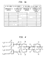
- differential amplifier 20 comprises a pair of capacitively-coupled differential amplifiers 21 and 23 as shown in Fig. 4; this is a conventional fully differential MOS version and has superior performance over the single-ended version shown in Fig. 1.
- a programmable resistor 24 is connected across the outputs of differential amplifier 21 and the inputs of differential amplifier 23 as shown in Fig. 4.
- the programmable resistor is implemented using a MOS operating in the triode region.
- the gain of the differential amplifier 20 is normally selected so that its output does not saturate in a given amount of time for a 0.5 LSB differential input.
- the "given amount of time" is determined by the speed of operation of the A/D converter.
- mode control circuit 16 turns off the resistor 74 to allow the highest possible gain.
- the resistor 74 is programmed to the value needed to present saturation.
- the operation of the reconfigurable A/D converter as shown in Fig. 1 will now be described.
- the fast mode when the control bits from mode control circuit 16 configure the A/D converter in its first operating mode, the interpolating latches 13 are disabled by setting the ENABLE signal input to these latches to low. However, the main latches 22 remain enabled. In addition, the proper clocking scheme is chosen for this mode of operation.
- the V in signal is input to comparators 19 and compared to the reference voltages, V ref .
- multiplexer (mux) 27 receives input from the comparator 19 every clock cycle.
- the thermometer code from mux 27 is encoded by encoder 24 and an N bit digital representation of V in is output.
- the control bits from mode control circuit 16 configure the A/D converter into its slow mode of operation, interpolating latches 13 are enabled, the gain of the differential amplifier is set, and the proper clocking scheme for this mode is chosen.
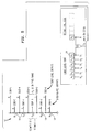
- the A/D converter uses two level encoding during the slow operating mode, 1.e., the mux 27 receives inputs from the comparator 19 and from latch 13, respectively, on alternate clock cycles. For example, during a first clock cycle, a first N-bit word is generated, and during a second clock cycle a second N-bit word is generated; the process is then repeated (see Fig. 5).
- the second N-bit word is either identical to the first N-bit word or is incremented by one, it is only necessary to look at the least significant bit (LSB) of the second N-bit word to determine the final N+1 bit output of the A/D converter. If the LSB bit of second N-bit word is the same as the first N-bit word, then the A/D converter 10 output will be the same as the first N bit word with a zero added to its LSB position to generate the N+1 bits; if they are different, then a 1 is added to the LSB position of the first N-bit word to obtain the N+1 bits.
- a symbolic representation of the two-level encoding is shown in Fig. 5.
- the first level encoding gives a six bit word that is equal to "000011” (output code equals 3) indicating that the input is in the example range.
- the second six bit word will be either "000011” indicating that the input is in SEGMENT I of the example (in which case the 7-bit word would be 0000110) or "000100” indicating that the input is in SEGMENT II of the example range (in which case the 7-bit word would be 0000111).
- the seventh bit is simply the EXCLUSIVE OR of the LSB bit of the two 6-bit words.
- the first level encoding corresponds to real comparator outputs and the second level encoding corresponds to the interpolating latches output
- additional hardware is required to implement the algorithm, since the results of the first level encoding would have to be stored separately.
- the sequence of encoding is reversed.
- the interpolating latch outputs are encoded and the resulting 6-bits are clocked into the output latches 25 (a series of flip-flop, for example) that are shown in Fig. 1.
- the LSB bit of the same 6-bit word is also held separately in a separate flip-flop 26.
- the comparator outputs 19 are encoded to form the second 6-bit word.
- bits also are latched into the output latches 25 of the encoder, thus over-writing the results of the first level encoding. These bits also represent the first six bits of the final 7-bit word.
- the seventh bit is generated by exclusive ORing the stored bit from first level encoding with the LSB bit of the second level encoding via XOR gate 28 and flip-flop 29, just as shown in Fig. 5, with the exception that the two passes are done in the reverse order.
- the reconfigurable A/D converter may be modified to provide more than two operating states (i.e., more than two level encoding).
- more than two operating states i.e., more than two level encoding.
- a three-state A/D converter that generates three N-bit words, one in each of its three states, is possible with the addition of a second set of differential amplifiers and interpolating latches.
- the reconfigurable A/D converter 10 in accordance with the present invention is ideally suited for use in a read channel circuit.
- the first operating mode of the A/D converter 10 is used during the user data mode and the second operating mode is used during the servo mode.
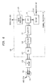
- FIG. 6 a schematic block diagram of a read channel device utilizing the reconfigurable flash A/D converter of the present convention is shown.
- the read channel device is indicated generally at 100.
- a first motor (not shown) spins the magnetic disks 114.
- a second motor (not shown) moves the read heads 116 in a radial direction with respect to the disks 114.
- the signal path used to demodulate the user data signal consists of a Low Noise Preamp (LNP) 109, a Variable Gain Amplifier (VGA) 102, a low-pass filter 104, an equalizer 111, a reconfigurable A/D converter 10, and a sequence detector 112.
- LNP Low Noise Preamp
- VGA Variable Gain Amplifier
- the signal path used to demodulate the servo data signal is the same as the path for the user data, up to the A/D converter 10. Instead of travelling through the sequence detector 112, however, the output of the A/D converter is sent to a digital servo demodulator 117 as shown.
- a command word indicates whether the signal to be detected by the read head is a user data signal or a servo signal (i.e., whether the read channel circuit is in the user data mode or the servo data mode).
- the channel processor circuit is constantly updating positioning information by switching between the servo mode and read data mode.
- the access and transfer rate is approximately 250 MHz in the user data mode and is approximately 80 MHz in the servo mode.
- the resolution of the A/D converter during the user data mode is six (6) bits while in the servo mode it is seven (7) bits.
- the reconfigurable A/D converter can be used during both modes of operation.
- the second level encoding within the A/D converter is similar to that of the read mode encoding. That is, after the servo data is read, the A/D converter 10 generates an N-bit word in a similar fashion as generated during the read mode. However, since the data transfer rate is slower during the servo mode, the A/D convertor 10 performs the second level encoding in the same time slot to generate the extra LSB forming an N+1 bit word.
- the servo mode can be described as an enhanced read mode. This means that all of the things that happen in the read mode also happen in the servo mode, and in addition, the interpolating latches 13 are powered up and the A/D clocking is internally modified to facilitate the operation of the interpolating latches 13 and the two level encoding.
- the interpolating latches 13 are enabled and the length of the thermometer code now will be 128, and these will be encoded by a single 64 input/6 output encoder as follows. First, the encoder encodes the 64 thermometer bits as it normally does in the user mode and the resulting 6 bits are then latched in a 6-bit register. Next, the two-input multiplexer 27 present at the input of the encoder 24 switches to connect the outputs of the interpolating latches 13 to the encoder 24 and a second 6-bit word is thus generated. The final 7-bit word is generated from these two 6-bit words as explained above.
- the encoder 24 In order to achieve this sequential two-pass encoding, the encoder 24 must be run at no higher than half the speed of the user mode. Since in the preferred embodiment, the A/D converter operates at 250 MHz in the user mode, the speed of the encoder presents no concern for the servo mode of operation up to 125 MHz. Since, typically, the servo mode speed is 80 MHz, the encoder 24 can make two passes in the same time slot that is allocated for encoding the thermometer code. This is, the same six-bit encoder is reused during a particular time slot.
- the use of the present invention simplifies the user and servo data processing and is less expensive to manufacture and to deploy than two separate A/D converters having different resolutions as is currently being used.
Landscapes
- Engineering & Computer Science (AREA)
- Theoretical Computer Science (AREA)
- Analogue/Digital Conversion (AREA)
- Read Only Memory (AREA)
Applications Claiming Priority (2)
| Application Number | Priority Date | Filing Date | Title |
|---|---|---|---|
| US08/866,094 US6175520B1 (en) | 1997-05-30 | 1997-05-30 | Nonvolatile memory array having local program load line repeaters |
| US866094 | 1997-05-30 |
Publications (2)
| Publication Number | Publication Date |
|---|---|
| EP0881776A2 true EP0881776A2 (fr) | 1998-12-02 |
| EP0881776A3 EP0881776A3 (fr) | 2002-08-07 |
Family
ID=25346902
Family Applications (1)
| Application Number | Title | Priority Date | Filing Date |
|---|---|---|---|
| EP98303942A Withdrawn EP0881776A3 (fr) | 1997-05-30 | 1998-05-19 | Convertisseur analogique-numérique reconfigurable |
Country Status (2)
| Country | Link |
|---|---|
| US (1) | US6175520B1 (fr) |
| EP (1) | EP0881776A3 (fr) |
Families Citing this family (1)
| Publication number | Priority date | Publication date | Assignee | Title |
|---|---|---|---|---|
| KR100595926B1 (ko) * | 1998-01-26 | 2006-07-05 | 웨인 웨스터만 | 수동 입력 통합 방법 및 장치 |
Family Cites Families (9)
| Publication number | Priority date | Publication date | Assignee | Title |
|---|---|---|---|---|
| US5206649A (en) * | 1987-07-20 | 1993-04-27 | Zdzislaw Gulczynski | Dual flash analog-to-digital converter |
| US4999812A (en) | 1988-11-23 | 1991-03-12 | National Semiconductor Corp. | Architecture for a flash erase EEPROM memory |
| US4928103A (en) * | 1989-09-18 | 1990-05-22 | Analog Devices, Inc. | Parallel analog-to-digital converter using 2.sup.(n-1) comparators |
| JP2595781B2 (ja) | 1990-07-13 | 1997-04-02 | 日本電気株式会社 | 半導体記憶装置 |
| US5598161A (en) * | 1992-12-18 | 1997-01-28 | Sony Corporation | Analog-to-digital converter having reduced circuit area |
| US5422842A (en) * | 1993-07-08 | 1995-06-06 | Sundisk Corporation | Method and circuit for simultaneously programming and verifying the programming of selected EEPROM cells |
| US5398203A (en) | 1993-09-01 | 1995-03-14 | Cypress Semiconductor Corporation | Memory programming load-line circuit with dual slope I-V curve |
| US5487033A (en) | 1994-06-28 | 1996-01-23 | Intel Corporation | Structure and method for low current programming of flash EEPROMS |
| US5469384A (en) * | 1994-09-27 | 1995-11-21 | Cypress Semiconductor Corp. | Decoding scheme for reliable multi bit hot electron programming |
-
1997
- 1997-05-30 US US08/866,094 patent/US6175520B1/en not_active Expired - Lifetime
-
1998
- 1998-05-19 EP EP98303942A patent/EP0881776A3/fr not_active Withdrawn
Also Published As
| Publication number | Publication date |
|---|---|
| EP0881776A3 (fr) | 2002-08-07 |
| US6175520B1 (en) | 2001-01-16 |
Similar Documents
| Publication | Publication Date | Title |
|---|---|---|
| US5877720A (en) | Reconfigurable analog-to-digital converter | |
| Flynn et al. | A 400-Msample/s, 6-b CMOS folding and interpolating ADC | |
| US7737875B2 (en) | Time interpolation flash ADC having automatic feedback calibration | |
| US9331706B1 (en) | High-speed analog-to-digital conversion system with flash assisted parallel SAR architecture | |
| US6459394B1 (en) | Multi-bank flash ADC array with uninterrupted operation during offset calibration and auto-zero | |
| US6445329B1 (en) | High speed analog to digital converter | |
| US5635934A (en) | Digital read channel utilizing analog-to-digital converter with offset reduction | |
| Sushihara et al. | A 7b 450MSample/s 50mW CMOS ADC in 0.3 mm/sup 2 | |
| US6329942B1 (en) | Parallel latch for high speed comparator using two modes of operation | |
| US7812745B2 (en) | Coding apparatus, decoding apparatus, amplitude adjustment apparatus, recorded information reader, signal processing apparatus and storage system | |
| US6078444A (en) | Read channel auxiliary high precision data conversion | |
| EP0881776A2 (fr) | Convertisseur analogique-numérique reconfigurable | |
| US6522489B1 (en) | Efficient analog-to-digital converter for digital systems | |
| CN101217281B (zh) | 一种超宽带系统的双采样两步式折叠内插模数转换器 | |
| USRE38719E1 (en) | Adjust bit determining circuit | |
| US6597302B2 (en) | System for increasing the bandwidth of sample-and-hold circuits in flash ADCs | |
| US6816096B2 (en) | Response-based analog-to-digital conversion apparatus and method | |
| JP4281909B2 (ja) | A/d変換回路とそれを用いたディスク再生システム | |
| JPH07336225A (ja) | Ad変換器 | |
| JP5090010B2 (ja) | 符号化装置 | |
| US6927713B2 (en) | Response-based analog-to-digital conversion apparatus and method | |
| JP2000235771A (ja) | ディジタルデータスライス回路 | |
| JP2666713B2 (ja) | 光ディスク装置 | |
| JPH06326609A (ja) | Adコンバータ及びディジタル信号再生処理装置 | |
| JP2626583B2 (ja) | アナログ/デジタル変換回路 |
Legal Events
| Date | Code | Title | Description |
|---|---|---|---|
| PUAI | Public reference made under article 153(3) epc to a published international application that has entered the european phase |
Free format text: ORIGINAL CODE: 0009012 |
|
| AK | Designated contracting states |
Kind code of ref document: A2 Designated state(s): AT BE CH CY DE DK ES FI FR GB GR IE IT LI LU MC NL PT SE |
|
| AX | Request for extension of the european patent |
Free format text: AL;LT;LV;MK;RO;SI |
|
| PUAL | Search report despatched |
Free format text: ORIGINAL CODE: 0009013 |
|
| AK | Designated contracting states |
Kind code of ref document: A3 Designated state(s): AT BE CH CY DE DK ES FI FR GB GR IE IT LI LU MC NL PT SE |
|
| AX | Request for extension of the european patent |
Free format text: AL;LT;LV;MK;RO;SI |
|
| AKX | Designation fees paid | ||
| STAA | Information on the status of an ep patent application or granted ep patent |
Free format text: STATUS: THE APPLICATION IS DEEMED TO BE WITHDRAWN |
|
| REG | Reference to a national code |
Ref country code: DE Ref legal event code: 8566 |
|
| 18D | Application deemed to be withdrawn |
Effective date: 20021202 |