EP0883185A1 - Selbstverstärkende DRAM-Zellenanordnung und Verfahren zu deren Herstellung - Google Patents
Selbstverstärkende DRAM-Zellenanordnung und Verfahren zu deren Herstellung Download PDFInfo
- Publication number
- EP0883185A1 EP0883185A1 EP98110034A EP98110034A EP0883185A1 EP 0883185 A1 EP0883185 A1 EP 0883185A1 EP 98110034 A EP98110034 A EP 98110034A EP 98110034 A EP98110034 A EP 98110034A EP 0883185 A1 EP0883185 A1 EP 0883185A1
- Authority
- EP
- European Patent Office
- Prior art keywords
- transistor
- source
- drain region
- trench
- flank
- Prior art date
- Legal status (The legal status is an assumption and is not a legal conclusion. Google has not performed a legal analysis and makes no representation as to the accuracy of the status listed.)
- Withdrawn
Links
- 238000000034 method Methods 0.000 title claims description 14
- 238000004519 manufacturing process Methods 0.000 title claims description 6
- 239000003990 capacitor Substances 0.000 claims description 42
- 229920002120 photoresistant polymer Polymers 0.000 claims description 29
- 239000000758 substrate Substances 0.000 claims description 22
- 239000002019 doping agent Substances 0.000 claims description 16
- 238000002513 implantation Methods 0.000 claims description 15
- 238000005530 etching Methods 0.000 claims description 13
- 125000006850 spacer group Chemical group 0.000 claims description 10
- 239000000463 material Substances 0.000 claims description 3
- 239000011810 insulating material Substances 0.000 claims 11
- 239000004020 conductor Substances 0.000 claims 5
- 238000002955 isolation Methods 0.000 claims 2
- 239000004065 semiconductor Substances 0.000 claims 2
- 210000000352 storage cell Anatomy 0.000 abstract 1
- 229910004298 SiO 2 Inorganic materials 0.000 description 29
- 229910021420 polycrystalline silicon Inorganic materials 0.000 description 14
- 229920005591 polysilicon Polymers 0.000 description 14
- BASFCYQUMIYNBI-UHFFFAOYSA-N platinum Chemical compound [Pt] BASFCYQUMIYNBI-UHFFFAOYSA-N 0.000 description 8
- 238000003860 storage Methods 0.000 description 7
- XUIMIQQOPSSXEZ-UHFFFAOYSA-N Silicon Chemical compound [Si] XUIMIQQOPSSXEZ-UHFFFAOYSA-N 0.000 description 6
- 238000000151 deposition Methods 0.000 description 6
- 229910052710 silicon Inorganic materials 0.000 description 6
- 239000010703 silicon Substances 0.000 description 6
- 229910052697 platinum Inorganic materials 0.000 description 4
- 239000003989 dielectric material Substances 0.000 description 3
- 229910052454 barium strontium titanate Inorganic materials 0.000 description 2
- 229910052751 metal Inorganic materials 0.000 description 2
- 239000002184 metal Substances 0.000 description 2
- 230000003647 oxidation Effects 0.000 description 2
- 238000007254 oxidation reaction Methods 0.000 description 2
- WFKWXMTUELFFGS-UHFFFAOYSA-N tungsten Chemical compound [W] WFKWXMTUELFFGS-UHFFFAOYSA-N 0.000 description 2
- 229910052721 tungsten Inorganic materials 0.000 description 2
- 239000010937 tungsten Substances 0.000 description 2
- 229910052782 aluminium Inorganic materials 0.000 description 1
- XAGFODPZIPBFFR-UHFFFAOYSA-N aluminium Chemical compound [Al] XAGFODPZIPBFFR-UHFFFAOYSA-N 0.000 description 1
- 238000003491 array Methods 0.000 description 1
- 230000008021 deposition Effects 0.000 description 1
- 238000005137 deposition process Methods 0.000 description 1
- 150000002739 metals Chemical class 0.000 description 1
- 238000012856 packing Methods 0.000 description 1
- 238000005498 polishing Methods 0.000 description 1
- 238000002360 preparation method Methods 0.000 description 1
- 229910021332 silicide Inorganic materials 0.000 description 1
Images



Classifications
-
- H—ELECTRICITY
- H10—SEMICONDUCTOR DEVICES; ELECTRIC SOLID-STATE DEVICES NOT OTHERWISE PROVIDED FOR
- H10B—ELECTRONIC MEMORY DEVICES
- H10B12/00—Dynamic random access memory [DRAM] devices
- H10B12/01—Manufacture or treatment
-
- H—ELECTRICITY
- H10—SEMICONDUCTOR DEVICES; ELECTRIC SOLID-STATE DEVICES NOT OTHERWISE PROVIDED FOR
- H10B—ELECTRONIC MEMORY DEVICES
- H10B12/00—Dynamic random access memory [DRAM] devices
-
- H—ELECTRICITY
- H10—SEMICONDUCTOR DEVICES; ELECTRIC SOLID-STATE DEVICES NOT OTHERWISE PROVIDED FOR
- H10B—ELECTRONIC MEMORY DEVICES
- H10B12/00—Dynamic random access memory [DRAM] devices
- H10B12/01—Manufacture or treatment
- H10B12/02—Manufacture or treatment for one transistor one-capacitor [1T-1C] memory cells
- H10B12/05—Making the transistor
- H10B12/053—Making the transistor the transistor being at least partially in a trench in the substrate
Definitions
- the invention relates to a DRAM cell arrangement, i.e. a Memory cell arrangement with dynamic random access, in which a memory cell comprises three transistors.
- DRAM cell arrays are currently used almost exclusively so-called one-transistor memory cells used.
- a single transistor memory cell includes a read transistor and one Storage capacitor.
- the information is in the storage capacitor stored in the form of an electrical charge that represents a logical quantity, 0 or 1. By control of the read transistor via a word line can this information can be read out via a bit line.
- the in Storage capacitor drives stored electrical charge the bit line.
- the storage capacitor despite the smaller area of the single transistor memory cell Minimum amount of electrical charge to be able to store to be able to drive the bit line.
- a second source / drain region of the first transistor is with a first source / drain region of the third transistor and a second source / drain region of the third transistor a reading bit line connected.
- a gate electrode of the third transistor via a readout Word line driven. The amount of electrical charge and with it the information, is about the reading bit line read out.
- the invention is based on the problem of a DRAM cell arrangement specify the gain cells as memory cells each with three transistors and particularly high Packing density can be produced.
- a manufacturing process is also intended can be specified for such a DRAM cell arrangement.
- a transistor of a memory cell as a vertical one Transistor formed. It is advantageous for all three transistors to design the memory cell as vertical transistors, because the area of the memory cell is particularly small becomes.
- the three transistors Flanks of a first trench and a second trench run essentially parallel to one another.
- the connection of the gate electrode of the first transistor, in which stores the information with the first source / drain region of the second transistor takes place via a conductive structure, for example, within the first Trench adjacent to a second flank on which none of the three transistors is formed.
- flanks of the first trenches and the second trenches between neighboring ones of a first conductivity type doped source / drain regions of various transistors no currents can flow through oblique implantation the flanks of the first trenches and the second trenches between generates highly doped channel stop regions for the transistors will.
- the channel stop areas are from a second to first conductivity type opposite conductivity type endowed.
- the information must be in regular New intervals on the gate electrodes of the first transistors to be written.
- a first substrate 1 made of silicon is p-doped in an approximately 2 ⁇ m thick layer S adjoining a surface O of the first substrate 1.
- the dopant concentration is approx. 10 17 cm -3 .
- the surface O comprises first areas B1 and second areas B2 (see FIGS. 1 and 2).
- the first areas B1 and the second areas B2 have the shape of approximately 0.5 ⁇ m wide strips and run parallel to one another.
- the first areas B1 and the second areas B2 are alternately arranged next to one another and adjoin one another.
- the first regions B1 comprise rectangular third regions B3 with a width of approximately 0.5 ⁇ m and a length of approximately 0.5 ⁇ m (see FIG. 1).
- the distance between the centers of adjacent third areas B3 of a first area B1 is approximately 2.25 ⁇ m .
- the smallest distance between adjacent third areas B3 of adjacent first areas B1 is approximately 1 ⁇ m .
- a first photoresist mask (not shown) which covers fourth regions B4 (see FIG. 1) which are approximately 1 ⁇ m long and approximately 0.5 ⁇ m wide and which are arranged within the second regions B2 between the third regions B3 .
- an n-doped approximately 150 nm deep region G is produced by implantation (see FIGS. 2a and 2b).
- the dopant concentration of the region G is approx. 5 * 10 20 cm -3 .
- a first insulating layer S1 made of SiO 2 is deposited on the surface O and structured with the aid of a second photoresist mask (not shown) by anisotropic etching (see FIGS. 2a and 2b).
- CHF 3 + O 2 is suitable as an etchant.
- Anisotropic etching of silicon selectively to SiO 2 produces first trenches G1 and second trenches G2 which run parallel to one another transversely to the first regions B1 and the second regions B2 (see FIGS. 2a and 2b).
- the structured first insulating layer S1 serves as a mask.
- HBrF is suitable as an etchant.
- the first trenches G1 and the second trenches G2 are approx.
- the shortest distance between the center line of a first trench G1 and the center of a third region B3 and the shortest distance between the center line of a second trench G2 and the center of a third region B3 are approximately 625 nm.
- Parts of the region remaining within the third regions B3 G are suitable as second source / drain regions 2S / D2 of second transistors and at the same time as second source / drain regions 3S / D2 of third transistors.
- Parts of the region G remaining within the first regions B1 between the third regions B3 are suitable as first source / drain regions 1S / D1 of first transistors.
- Parts of the region G remaining within the second regions B2 connect first source / drain regions 1S / D1 of first transistors adjacent along the second trenches G2.
- first channel stop areas C1 are produced by implantation (see FIG. 2a).
- the implantation takes place obliquely so that the first channel stop regions C1 adjoin second flanks 1F2 of the first trenches G1 and parts of first flanks 2F1 of the second trenches G2 located within the second regions B2.
- the width of the first channel stop regions C1 is approximately 100 nm.
- the dopant concentration of the first channel stop regions C1 is approximately 10 19 cm . 3rd
- p-doped second channel stop areas C2 are produced by implantation (see FIG. 2b).
- the implantation takes place obliquely, so that the second channel stop regions C2 adjoin first flanks 1F1 of the first trenches G1 and the second flanks 2F2 of the second trenches G2.
- the width of the second channel stop regions C2 is approximately 100 nm.
- the dopant concentration of the second channel stop regions C2 is approximately 10 9 cm -3 .
- first source / drain regions 2S / D1 of the second transistors adjacent to the bottoms of the first trenches G1 and first sources / adjacent to the bottoms of the second trenches G2 are implanted.
- Drain regions 3S / D1 of the third transistors, which are simultaneously second source / drain regions 1S / D2 of the first transistors, are produced (see FIG. 4).
- a subsequent RTP process activates the dopant of the first source / drain region 2S / D1 of the second transistor and of the first source / drain region 3S / D1 of the third transistor.
- the first source / drain region 2S / D1 of the second transistor and the first source / drain region 3S / D1 of the third transistor are n-doped and have a dopant concentration of approximately 5 * 10 20 cm -3 .
- a gate dielectric Gd is generated by thermal oxidation, that the first edges 1F1, the second edges 1F2 and a bottom of the first trench G1 and the first flanks 1F2, the second flanks 2F2 and a bottom of the second trench G2 covered (see Fig. 3).
- doped polysilicon with a thickness of approximately 150 nm is deposited and etched back, so that spacers are formed on the flanks of the first trench G1 and the second trench G2 (see FIGS. 3, 4).
- C 2 F 6 + O 2 is suitable as an etchant.
- Spacers on the first flanks 1F1 of the first trenches G1 act as writing word lines WS.
- Spacers on the first flanks 2F1 of the second trenches G2 act as read word lines WA.
- a sixth photoresist mask (not shown) which does not cover the second flanks 1F2 of the first trenches G1 and the second flanks 2F2 of the second trenches G2 in the second regions B2
- second parts of spacers are removed by etching polysilicon, so that Gate electrodes Ga1 are insulated from one another by first transistors adjacent along the second trenches G2 (see FIGS. 3 and 4).
- Spacers that adjoin the first channel stop regions C1 and the second channel stop regions C2 cannot, due to the high dopant concentration of the first channel stop regions C1 and the second channel stop regions C2, channel currents in the trigger first channel stop areas C1 and in the second channel stop areas C2. Channel areas of adjacent second transistors and channel areas of adjacent third transistors are thereby separated from one another.
- first trenches G1 and the second trenches G2 are filled with SiO 2 by depositing SiO 2 and then etching back isotropically (see FIG. 4).
- SiO 2 is deposited with a thickness of approx. 250 nm and then with the aid of a seventh photoresist mask (not shown) which does not cover the second flanks 1F2 of the first trenches G1 and the second flanks 2F2 of the second trenches G2 within the first regions B1. etched, which creates a second insulating structure I2 (see FIG. 4).
- an eighth photoresist mask (not shown), which does not cover the second flanks 1F2 of the first trenches G1 within the first areas B1, first polysilicon with, for example, C 2 F 6 + O 2 and then SiO 2 with, for example, CHF 3 + O 2 etched so that spacers on the second flanks 1F2 of the first trenches G1 are removed and a part of the bottom of the first trenches G1 is exposed.
- a third insulating structure I3 is then produced by depositing SiO 2 with a thickness of approximately 500 nm and etching using a tenth photoresist mask (not shown), which does not cover the third regions B3, until parts of the second source / drain Regions 3S / D2 of the third transistors are exposed (see FIG. 6). Then, for example, tungsten is deposited and etched back, whereby first contacts K1 of bit lines B to be generated are created.
- SF 6 for example, is suitable as an etchant.
- the bit lines B are strip-shaped and run parallel to one another transversely to the writing word lines WS and reading word lines WA.
- bit lines B e.g. aluminum deposited and then using an eleventh photoresist mask (not shown) covering the second areas B2 not covered, structured (see Fig. 6).
- a second substrate 1 ′ made of silicon is p-doped in an approximately 2 ⁇ m thick layer S ′ adjacent to a surface O ′ of the second substrate 1 ′.
- the dopant concentration is approximately 10 17 cm -3.
- the surface O 'of the second substrate 1' comprises first areas and second areas.
- the first areas comprise third areas and the second areas fourth areas.
- an n-doped region about 150 nm deep is generated by implantation.
- An approximately 150 nm thick first insulating layer S1 'made of SiO 2 is then deposited.
- a conductive layer SL 'made of polysilicon is deposited over this.
- An approximately 200 nm thick second insulating layer S2 'made of SiO 2 is deposited over this (see FIG. 7).
- gate electrodes Ga1 ' are isolated from one another by means of a sixth photoresist mask from first transistors which are adjacent along the second trenches G2'.
- the first trenches G1 'and the second trenches G2' are then filled with a first insulating structure I1 'made of SiO 2 .
- a twelfth photoresist mask (not shown), which covers the second flanks of the first trenches G1 'and the second flanks of the second trenches G2' in the first regions, polysilicon is selectively etched to SiO 2 (see FIG. 8).
- a second insulating structure I2 ' is then produced by depositing SiO 2 and using a thirteenth photoresist mask (not shown), which does not cover the second flanks of the first trenches G1' in the first regions, until a portion of the SiO 2 is etched conductive layer SL 'is exposed. Polysilicon is then etched and then SiO 2 again, so that parts of the bottoms of the first trenches G1 'are exposed. Subsequently, doped polysilicon with a thickness of approx.
- bit lines and first contacts generated by bit lines.
- a third substrate 1 ′′ made of silicon is p-doped in an approximately 2 ⁇ m thick layer S ′′ adjoining a surface O ′′ of the third substrate 1 ′′.
- the dopant concentration is approx. 10 17 cm -3 .
- the surface O ′′ comprises first areas and second areas.
- the first regions comprise third regions and the second regions fourth regions. Without a mask, an n-doped region about 150 nm deep is produced by implantation.
- a first insulating layer S1 ′′ made of SiO 2 , a conductive layer SL ′′ made of polysilicon, a second insulating layer made of SiO 2 , first trenches G1 ′′ and second trenches G2 ′′ are subsequently produced (see FIG. Figure 10).
- SiO 2 is then deposited and etched back, as a result of which the first trenches and the second trenches are filled with SiO 2 (see FIG. 10).
- a thirteenth photoresist mask With the help of a thirteenth photoresist mask, the fourth regions not covered, first SiO 2, then polysilicon and then etched SiO 2, so that parts of the surface are exposed.
- the thirteenth photoresist mask is removed.
- Wells are then created by selectively etching silicon to SiO 2 to a depth of approximately 300 nm. Remaining parts of the region G ′′ are suitable as second source / drain regions of second transistors, second source / drain regions of third transistors and as first source / drain regions of first transistors.
- SiO 2 is then etched so that the flanks and the bottoms of the first trenches G1 ′′ and the second trenches G2 ′′ are exposed.
- the second flanks of the first in the second areas Trenches and the second flanks of the second trenches and the third areas and parts of the fourth areas not covered polysilicon is etched, causing gate electrodes of first transistors adjacent along the second trenches and second source-drain regions each from along the second trenches adjacent second transistors from each other be isolated.
- bit lines are analogous to the second embodiment conductive structures, bit lines and first contacts of bit lines generated.
- capacitors can be used to be built in. This is done in a fourth embodiment explained. Analogous to the first embodiment first trenches G1 *, second trenches G2 *, first Source / drain regions 1S / D1 * of first transistors, second Source / drain regions 3S / D2 * of third transistors, second Source / drain regions 2S / D2 * of second transistors, first Channel stop areas C1 *, second channel stop areas, first Source / drain regions 2S / D1 * of the second transistors, first Source / drain regions 3S / D1 * of the third transistors, second Source / drain regions 1S / D2 * of the first transistors, a gate dielectric Gd *, gate electrodes Ga1 * of the first transistors, Gate electrodes Ga2 * of the second transistors, gate electrodes Ga3 * of the third transistors, writing word lines, read word lines, a first insulating structure I1 *, a second insulating structure I2 * and conductive
- Second insulating layer S2 * is then produced by depositing SiO 2 .
- SiO 2 is etched until the parts of the horizontal ones Elements Lh * of the conductive structures L * above the first source / drain regions 1S / D1 * of the first transistors are exposed.
- second contacts K2 * of first capacitor plates P1 * to be produced are produced, for example by depositing and etching back tungsten.
- platinum with a thickness of approx. 200 nm is deposited.
- a sixteenth photoresist mask (not shown) the parts of the second insulating layer S2 * within the first regions above the second source / drain regions 2S / D2 * of the second transistors and the second source / drain regions 3S / D2 * of the third transistor is not covered, platinum is etched with, for example, Cl 2 + O 2 , whereby the first capacitor plates P1 * are produced.
- barium strontium titanate is deposited with a thickness of approx. 20 nm and platinum is deposited over it with a thickness of approx. 200 nm.
- a seventeenth photoresist mask (not shown) which does not cover the strip-shaped regions which run parallel to the first trenches and are arranged between the first contacts K1 * and which comprise the first capacitor plates P1 *, platinum and barium strontium titanate with, for example, Cl 2 are simultaneously covered + O 2 etched, creating second capacitor plates P2 * and capacitor dielectrics Kd *.
- third insulating structure I3 * first contacts K1 * of bit lines B * and bit lines B * are generated.
- the dimensions of the layers, areas, areas and trenches described can be adapted to the respective requirements.
- Structures and layers made of SiO 2 can be produced in particular by thermal oxidation or by a deposition process.
- Polysilicon can be doped both during and after the deposition.
- metal silicides and / or metals can also be used, for example.
- Particularly suitable materials for the capacitor dielectrics are dielectrics with high dielectric constants, such as, for example, perovskites.
- chemical-mechanical polishing can also be used to produce the first insulating structure and then slightly overetched. The same applies to the creation of the conductive structure.
Landscapes
- Engineering & Computer Science (AREA)
- Manufacturing & Machinery (AREA)
- Semiconductor Memories (AREA)
Abstract
Description
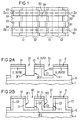
- Figur 1
- zeigt eine Oberfläche eines ersten Substrats, die in erste Bereiche, die dritte Bereiche umfassen, und zweite Bereiche, die vierte Bereiche umfassen, unterteilt ist. Es wurden erste Gräben und zweite Gräben erzeugt.
- Figur 2a
- zeigt einen ersten Querschnitt entlang der Mittellinie eines ersten Bereichs durch das in einer Schicht dotierte erste Substrat, nachdem eine erste isolierende Schicht, erste Gräben, zweite Gräben, erste Source/Drain-Gebiete von ersten Transistoren, zweite Source/Drain-Gebiete von zweiten Transistoren, zweite Source/Drain-Gebiete von dritten Transistoren, erste Channel-Stop-Gebiete und zweite Channel-Stop-Gebiete erzeugt wurden.
- Figur 2b
- zeigt das Substrat aus Figur 2a in einem zum ersten Querschnitt parallelen zweiten Querschnitt entlang der Mittellinie eines der zweiten Bereiche.
- Figur 3
- zeigt den Querschnitt aus Figur 2b, nachdem erste Source/Drain-Gebiete der zweiten Transistoren, erste Source/Drain-Gebiete der dritten Transistoren, zweite Source/Drain-Gebiete der ersten Transistoren, ein Gatedielektrikum, Gateelektroden der ersten Transistoren, Gateelektroden der zweiten Transistoren und Gateelektroden der dritten Transistoren erzeugt wurden.
- Figur 4
- zeigt den Querschnitt aus Figur 2a, nachdem erste Source/Drain-Gebiete der zweiten Transistoren, erste Source/Drain-Gebiete der dritten Transistoren, zweite Source/Drain-Gebiete der ersten Transistoren, ein Gatedielektrikum, erste Gateelektroden, Gateelektroden der zweiten Transistoren, Gateelektroden der dritten Transistoren, eine erste isolierende Struktur und eine zweite isolierende Struktur erzeugt wurden.
- Figur 5
- zeigt den Querschnitt aus Figur 4, nachdem leitende Strukturen, die jeweils eine Gateelektrode eines ersten Transistors mit einem ersten Source/Drain-Gebiet eines zweiten Transistors verbindet, erzeugt wurden.
- Figur 6
- zeigt den Querschnitt aus Figur 5, nachdem Bitleitungen und Kontakte der Bitleitungen erzeugt wurden.
- Figur 7
- zeigt einen zum Querschnitt in Figur 2a analogen Querschnitt durch ein in einer Schicht dotiertes zweites Substrat, nachdem ein erstes Gebiet implantiert wurde und eine erste isolierende Schicht, eine leitende Schicht und eine zweite isolierende Schicht abgeschieden wurden.
- Figur 8
- zeigt den Querschnitt aus Figur 7, nachdem erste Gräben, zweite Gräben, erste Source/Drain-Gebiete der ersten Transistoren, zweite Source/Drain-Gebiete der zweiten Transistoren, zweite Source/Drain-Gebiete der dritten Transistoren, Channel-Stop-Gebiete, erste Source/Drain-Gebiete der zweiten Transistoren, erste Source/Drain-Gebiete der dritten Transistoren, zweite Source/Drain-Gebiete der ersten Transistoren, ein Gatedielektrikum, Gateelektroden der ersten Transistoren, Gateelektroden der zweiten Transistoren, Gateelektroden der dritten Transistoren und eine erste isolierende Struktur erzeugt wurden.
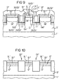
- Figur 9
- zeigt den Querschnitt aus Figur 8, nachdem eine zweite isolierende Struktur und eine leitende Struktur erzeugt wurden.
- Figur 10
- zeigt einen zum Querschnitt aus Figur 2b analogen Querschnitt durch ein drittes Substrat, nachdem eine erste isolierende Schicht, eine leitende Schicht und mit SiO 2 gefüllte erste Gräben und zweite Gräben erzeugt wurden.
- Figur 11
- zeigt den Querschnitt aus Figur 11, nachdem Vertiefungen erzeugt wurden.
- Figur 12
- zeigt einen zum Querschnitt aus Figur 6 analogen Querschnitt durch ein viertes Substrat nach Fertigstellung der DRAM-Zellenanordnung, deren Speicherzellen jeweils drei vertikale Transistoren und einen Kondensator umfassen.
Claims (20)
- DRAM-Zellenanordnung,mit Speicherzellen, die jeweils einen ersten Transistor, einen zweiten Transistor und einen dritten Transistor umfassen,bei der eine Gateelektrode (Ga1) des ersten Transistors mit einem ersten Source/Drain-Gebiet (2S/D1) des zweiten Transistors verbunden ist,bei der ein zweites Source/Drain-Gebiet (2S/D2) des zweiten Transistors mit einer schreibenden Bitleitung (B) verbunden ist,bei der eine Gateelektrode (Ga2) des zweiten Transistors mit einer schreibenden Wortleitung (WS) verbunden ist,bei der eine Gateelektrode (Ga3) des dritten Transistors mit einer auslesenden Wortleitung (WA) verbunden ist,bei der ein zweites Source/Drain-Gebiet (1S/D2) des ersten Transistors mit einem ersten Source/Drain-Gebiet (3S/D1) des dritten Transistors verbunden ist,bei der ein zweites Source/Drain-Gebiet (3S/D2) des dritten Transistors mit einer auslesenden Bitleitung (B) verbunden ist, dadurch gekennzeichnet, daßder erste Transistor, der zweite Transistor und der dritte Transistor vertikale MOS-Transistoren sind.
- DRAM-Zellenanordnung nach Anspruch 1,bei der eine erste Flanke eines in einem Substrat (1) aus Halbleitermaterial befindlichen ersten Grabens (G1) mit einem Gatedielektrikum (Gd) versehen ist,bei der eine erste Flanke eines zweiten Grabens (Ga2) mit dem Gatedielektrikum (Gd) versehen ist,bei der der erste Graben (G1) und der zweite Graben (G2) im wesentlichen parallel verlaufen,bei der die schreibende Wortleitung (WS) entlang des ersten Grabens (G1) verläuft,bei der die auslesende Wortleitung (WA) entlang des zweiten Grabens (G2) verläuft,bei der die Gateelektrode (Ga2) des zweiten Transistors innerhalb des ersten Grabens (G1) an die erste Flanke (1F1) des ersten Grabens (G1) angrenzt,bei der die Gateelektrode (Ga3) des dritten Transistors innerhalb des zweiten Grabens (G2) an eine erste Flanke (2F1) des zweiten Grabens (Ga2) angrenzt.
- DRAM-Zellenanordnung nach Anspruch 2,bei der das erste Source/Drain-Gebiet (2S/D1) des zweiten Transistors an einen Boden des ersten Grabens (G1) angrenzt,bei der das erste Source/Drain-Gebiet (3S/D1) des dritten Transistors an einen Boden des zweiten Grabens (G2) angrenzt,bei der das zweite Source/Drain-Gebiet (2S/D2) des zweiten Transistors seitlich an die erste Flanke (1F1) des ersten Grabens (G1) angrenzt,bei der das zweite Source/Drain-Gebiet (3S/D2) des dritten Transistors seitlich an die erste Flanke (2F1) des zweiten Grabens (G2) angrenzt,bei der die schreibende Bitleitung (B) und die auslesende Bitleitung (B) quer zu der schreibenden Wortleitung (WS) und der auslesenden Wortleitung (WA) verlaufen,bei der die schreibende Bitleitung (B) oberhalb zweiter erster Source/Drain-Gebiete (2S/D1) und die auslesende Bitleitung (B) oberhalb erster Source/Drain-Gebiete (3S/D1) von dritten Transistoren angeordnet sind.
- DRAM-Zellenanordnung nach Anspruch 3,bei der die Gateelektrode (Ga1) des ersten Transistors an eine zweite Flanke (2F2) des zweiten Grabens (G2) angrenzt und innerhalb des zweiten Grabens (G2) angeordnet ist,bei der die zweite Flanke (2F2) des zweiten Grabens (G2) mit dem Gatedielektrikum (Gd) versehen ist,bei der das erste Source/Drain-Gebiet (3S/D1) des dritten Transistors mit dem zweiten Source/Drain-Gebiet (1S/D2) des ersten Transistors zusammenfällt,bei der ein erstes Source/Drain-Gebiet (1S/D1) des ersten Transistors seitlich an die zweite Flanke (2F2) des zweiten Grabens (G2) angrenzt,bei der die Gateelektrode (Ga1) des ersten Transistors mit dem ersten Source/Drain-Gebiet (2S/D1) des zweiten Transistors über eine leitende Struktur (L) verbunden ist,bei der die leitende Struktur (L) ein horizontales Element (Lh) und ein vertikales Element (Lv) umfaßt,bei der das horizontale Element (Lh) über einem ersten Teil einer ersten isolierenden Schicht (S1), der über dem ersten Source/Drain-Gebiet (1S/D1) des ersten Transistors angeordnet ist, angeordnet ist,bei der das vertikale Element (Lv) an eine zweite Flanke (1F2) des ersten Grabens (G1) angrenzt und innerhalb des ersten Grabens (G1) angeordnet ist,bei der die auslesende Bitleitung (B) mit der schreibenden Bitleitung (B) zusammenfällt.
- DRAM-Zellenanordnung nach Anspruch 4,bei der das erste Source/Drain-Gebiet (1S/D1) des ersten Transistors seitlich an die zweite Flanke (1F2) des ersten Grabens (G1) angrenzt,bei der das erste Source/Drain-Gebiet (1S/D1) des ersten Transistors, das zweite Source/Drain-Gebiet (1S/D2) des ersten Transistors, das erste Source/Drain-Gebiet (2S/D1) des zweiten Transistors, das zweite Source/Drain-Gebiet (2S/D2) des zweiten Transistors, das erste Source/Drain-Gebiet (3S/D1) des dritten Transistors und das zweite Source/Drain-Gebiet (3S/D2) des dritten Transistors von einem ersten Leitfähigkeitstyp dotiert sind,bei der das Substrat (1) in einer an eine Oberfläche (O) des Substrats (1) angrenzenden Schicht (S) von einem zweiten, zum ersten Leitfähigkeitstyp entgegengesetzten Leitfähigkeitstyp dotiert ist,bei der die Schicht (S) eine erste Dotierstoffkonzentration aufweist,bei der ein erstes Channel-Stop-Gebiet (C1) an die zweite Flanke des ersten Grabens (G1) angrenzt und im Substrat (1) angeordnet ist,bei der die zweite Flanke des ersten Grabens (G1) mit dem Gatedielektrikum (Gd) versehen ist,bei der das erste Channel-Stop-Gebiet (C1) vom zweiten Leitfähigkeitstyp dotiert ist und eine zweite Dotierstoffkonzentration aufweist, die höher als die erste Dotierstoffkonzentration ist.
- DRAM-Zellenanordnung nach einem der Ansprüche 1 bis 5, bei der benachbarte zweite Source/Drain-Gebiete (2S/D2) von zweiten Transistoren und benachbarte zweite Source/Drain-Gebiete (3S/D2) von dritten Transistoren jeweils durch eine mit isolierendem Material gefüllte Vertiefung voneinander isoliert sind.
- DRAM-Zellenanordnung nach einem der Ansprüche 1 bis 6,bei der Speicherzellen jeweils einen Kondensator umfassen,bei der der Kondensator eine erste Kondensatorplatte (P1*), eine zweite Kondensatorplatte (P1*) und ein zwischen der ersten Kondensatorplatte und der zweiten Kondensatorplatte (P2*) angeordnetes Kondensatordielektrikum (Kd*) umfaßt,bei der die erste Kondensatorplatte (P1*) mit dem ersten Source/Drain-Gebiet (1 S/D1*) des ersten Transistors verbunden ist.
- DRAM-Zellenanordnung nach Anspruch 7,bei der die erste Kondensatorplatte (P1*) über einen zweiten Kontakt (K2*) mit dem ersten Source/Drain-Gebiet (1S/D1*) des ersten Transistors verbunden und oberhalb des ersten Source/Drain-Gebiets (1S/D1*) des ersten Transistors angeordnet ist,bei der die zweite Kondensatorplatte (P2*) oberhalb der ersten Kondensatorplatte (P1*) und unterhalb der Bitleitung (B*) angeordnet ist,bei der zweite Kondensatorplatten (P2*) von entlang des ersten Grabens (G1*) benachbarten Kondensatoren verbunden sind.
- Verfahren zur Herstellung einer DRAM-Zellenanordnung,bei dem Speicherzellen, die jeweils einen ersten Transistor, einen zweiten Transistor und einen dritten Transistor umfassen, erzeugt werden,bei dem schreibende Wortleitungen (WS) und auslesende Wortleitungen (WA) und quer zu den schreibenden Wortleitungen (WS) und den auslesenden Wortleitungen (WA) schreibende Bitleitungen (B) und auslesende Bitleitungen (B) erzeugt werden,bei dem Gateelektroden, erste Source/Drain-Gebiete und zweite Source/Drain-Gebiete erzeugt werden,bei dem eine Gateelektrode (Ga1) des ersten Transistors mit einem ersten Source/Drain-Gebiet (2S/D1) des zweiten Transistors verbunden wird,bei dem ein zweites Source/Drain-Gebiet (2S/D2) des zweiten Transistors mit einer schreibenden Bitleitung (B) verbunden wird,bei dem eine Gateelektrode (Ga2) des zweiten Transistors mit einer schreibenden Wortleitung (WS) verbunden wird,bei dem eine Gateelektrode (Ga3) des dritten Transistors mit einer auslesenden Wortleitung (WA) verbunden wird,bei dem ein zweites Source/Drain-Gebiet (1S/D2) des ersten Transistors mit einem ersten Source/Drain-Gebiet (3S/D1) des dritten Transistors verbunden wird,bei dem ein zweites Source/Drain-Gebiet (3S/D2) des dritten Transistors mit einer auslesenden Bitleitung (B) verbunden wird,bei dem der erste Transistor, der zweite Transistor und der dritte Transistor als vertikale Transistoren gebildet werden.
- Verfahren nach Anspruch 9,bei dem in einem Substrat (1) erste Gräben (G1) und zweite Gräben (G2) erzeugt werden, die im wesentlichen parallel zueinander verlaufen,bei der erste Flanken (1F1) der ersten Gräben (G1) und erste Flanken (2F1) der zweiten Gräben (G2) mit einem Gatedielektrikum (Gd) versehen werden,bei dem die Gateelektrode (Ga2) des zweiten Transistors innerhalb eines ersten Grabens (G1) als Spacer an eine erste Flanke (1F1) des ersten Grabens (G1) angrenzend gebildet wird,bei dem die schreibende Wortleitung (WS) entlang des ersten Grabens (G1) verläuft,bei dem die Gateelektrode (Ga3) des dritten Transistors innerhalb eines zweiten Grabens (G2) als Spacer an die erste Flanke (2F1) des zweiten Grabens (G2) angrenzend gebildet wird,bei dem die auslesende Wortleitung (WA) entlang des zweiten Grabens (G1) verläuft.
- Verfahren nach Anspruch 10,bei dem das erste Source/Drain-Gebiet (2S/D1) des zweiten Transistors so erzeugt wird, daß es an einen Boden des ersten Grabens (G1) angrenzt,bei dem das erste Source/Drain-Gebiet (3S/D1) des dritten Transistors so erzeugt wird, daß es an einen Boden des zweiten Grabens (G2) angrenzt,bei dem das zweite Source/Drain-Gebiet (2S/D2) des zweiten Transistors so erzeugt wird, daß es seitlich an die erste Flanke (1F1) des ersten Grabens (G1) angrenzt,bei der das zweite Source/Drain-Gebiet (3S/D2) des dritten Transistors so erzeugt wird, daß es seitlich an die erste Flanke (2F1) des zweiten Grabens (G2) angrenzt,bei dem die schreibende Bitleitung (B) und die auslesende Bitleitung (B) so erzeugt werden, daß sie quer zu der schreibenden Wortleitung (WS) und der auslesenden Wortleitung (WA) verlaufen,bei dem die schreibende Bitleitung (B) oberhalb erster Source/Drain-Gebiete (2S/D1) von zweiten Transistoren und die auslesende Bitleitung (B) oberhalb erster Source/Drain-Gebiete (3S/D1) von dritten Transistoren gebildet werden.
- Verfahren nach Anspruch 11,bei dem die zweite Flanke (2F2) des zweiten Grabens (G2) mit dem Gatedielektrikum (Gd) versehen wird,bei dem die Gateelektrode (Ga1) des ersten Transistors innerhalb des zweiten Grabens (G2) an eine zweite Flanke (2F2) des zweiten Grabens (G2) angrenzend gebildet wird,bei dem das zweite Source/Drain-Gebiet (2S/D2) des zweiten Transistors so erzeugt wird, daß es an den Boden des ersten Grabens (G1) angrenzt,bei dem ein erstes Source/Drain-Gebiet (1S/D1) des ersten Transistors so erzeugt wird, daß es seitlich an die zweite Flanke (2F2) des zweiten Grabens (G2) angrenzt,bei dem über dem ersten Source/Drain-Gebiet (1S/D1) des ersten Transistors ein horizontales Element (Lh) einer leitenden Strukur (L) erzeugt wird, und zwar so, daß es mit der Gateelektrode (Ga1) des ersten Transistors verbunden wird,bei dem an eine zweite Flanke (1F2) des ersten Grabens (G1) angrenzend ein Gatedielektrikum (Gd) erzeugt wird,bei dem an die zweite Flanke (1F2) des ersten Grabens (G1) angrenzend innerhalb des ersten Grabens (G1) ein vertikales Element (Lv) der leitenden Struktur (L) erzeugt wird, und zwar so, daß es mit dem ersten Source/Drain-Gebiet (2S/D1) des zweiten Transistors und dem horizontalen Element (Lh) der leitenden Struktur (L) verbunden wird,bei dem Bitleitungen (B) erzeugt werden, die jeweils sowohl als die auslesende Bitleitung (B) als auch als die schreibende Bitleitung (B) dienen.
- Verfahren nach Anspruch 12,bei dem das Substrat (1), das Halbleitermaterial enthält, in einer an eine Oberfläche (O) des Substrats (1) angrenzenden Schicht (S) von einem zweiten Leitfähigkeitstyp mit einer ersten Dotierstoffkonzentration dotiert wird,bei dem das erste Source/Drain-Gebiet (1S/D1) des ersten Transistors so gebildet wird, daß es seitlich an die zweite Flanke (1F2) des ersten Grabens (G1) angrenzt,bei dem ein zweites Source/Drain-Gebiet (3S/D2) des dritten Transistors einer ersten Speicherzelle und ein zweites Source/Drain-Gebiet (2S/D2) des zweiten Transistors einer benachbarten zweiten Speicherzelle so gebildet werden, daß sie aneinander angrenzen oder zusammenfallen,bei dem in dem Substrat (1) das erste Source/Drain-Gebiet (1S/D1) des ersten Transistors, das zweite Source/Drain-Gebiet (1S/D2) des ersten Transistors, das erste Source/Drain-Gebiet (2S/D1) des zweiten Transistors, das zweite Source/Drain-Gebiet (2S/D2) des zweiten Transistors, das erste Source/Drain-Gebiet (3S/D1) des dritten Transistors und das zweite Source/Drain-Gebiet (3S/D2) des dritten Transistors durch Implantation erzeugt werden, und zwar so, daß sie von einem ersten, zum zweiten Leitfähigkeitstyp entgegengesetzten Leitfahigkeitstyp dotiert werden,bei dem außerhalb des ersten Grabens (G1) an die zweite Flanke des ersten Grabens (G1) angrenzend durch Implantation ein vom zweiten Leitfähigkeitstyp dotiertes erstes Channel-Stop-Gebiet (C1) erzeugt wird, so, daß es eine zweite Dotierstoffkonzentration aufweist, die höher als die erste Dotierstoffkonzentration ist,bei dem die Bitleitung (B) oberhalb des ersten Source/Drain-Gebiets (1S/D1) des ersten Transistors, des zweiten Source/Drain-Gebiets (1S/D2) des ersten Transistors, des ersten Source/Drain-Gebiets (2S/D1) des zweiten Transistors, des zweiten Source/Drain-Gebiets (2S/D2) des zweiten Transistors, des ersten Source/Drain-Gebiets (3S/D1) des dritten Transistors und das zweiten Source/Drain-Gebiets des dritten Transistors (3S/D2) verläuft.
- Verfahren nach Anspruch 13bei dem in der Schicht (S) des Substrats (1) ein vom ersten Leitfähigkeitstyp dotiertes Gebiet (G) erzeugt wird,bei dem auf der Oberfläche (O) isolierendes Material aufgebracht und geätzt wird, so, daß eine strukturierte erste isolierende Schicht (S1) entsteht,bei dem aus dem Gebiet (G) durch die Erzeugung der ersten Gräben (G1) und der zweiten Gräben (G2) das erste Source/Drain-Gebiet (1S/D1) des ersten Transistors, das zweite Source/Drain-Gebiet (2S/D2) des zweiten Transistors und das zweite Source/Drain-Gebiet (3S/D2) des dritten Transistors entstehen,bei dem nach der Erzeugung des ersten Grabens (G1) und des zweiten Grabens (G2) das erste Channel-Stop-Gebiet (C1) durch schräge Implantation erzeugt wird,bei dem nach der Erzeugung des ersten Channel-Stop-Gebiets (C1) bei der Implantation des ersten Source/Drain-Gebietes (3S/D1) des dritten Transistors, des zweiten Source/Drain-Gebietes (1S/D2) des ersten Transistors und des ersten Source/Drain-Gebietes (2S/D1) des zweiten Transistors eine streifenförmige fünfte Photolackmaske verwendet wird, die zwischen benachbarten Bitleitungen (B) liegende zweite Bereiche (B2) vor Implantation schützt,bei dem zur Erzeugung der Gateelektrode (Ga1) des ersten Transistors, der Gateelektrode (Ga2) des zweiten Transistors und der Gateelektrode (Ga3) des dritten Transistors nach der Erzeugung des Gatedielektrikums (Gd), leitendes Material abgeschieden und rückgeätzt wird, so daß die Gateelektrode (Ga1) des ersten Transistors, die Gateelektrode (Ga2) des zweiten Transistors und die Gateelektrode (Ga3) des dritten Transistors in Form von Spacern entstehen,bei dem mit Hilfe einer sechsten Photolackmaske entlang der zweiten Gräben (G2) benachbarte erste Gateelektroden (Ga1) durch Ätzen des leitenden Materials voneinander isoliert werden,bei dem der erste Graben (G1) und der zweite Graben (G2) anschließend mit isolierendem Material aufgefüllt werden,bei dem nach der Erzeugung der leitenden Struktur (L) eine dritte isolierende Struktur (I3) aus isolierendem Material erzeugt wird, indem mit Hilfe einer zehnten Photolackmaske isolierendes Material geätzt wird, so, daß das zweite Source/Drain-Gebiet (3S/D2) des dritten Transistors und das zweite Source/Drain-Gebiet (2S/D2) des zweiten Transistors teilweise freigelegt werden,bei dem anschließend leitendes Material aufgebracht wird und mit Hilfe einer elften Photolackmaske so strukturiert wird, daß die Bitleitungen (B) und Kontakte (K) der Bitleitungen (B) entstehen.
- Verfahren nach Anspruch 14,bei dem nach der Erzeugung der ersten isolierenden Struktur (I1) eine zweite isolierende Struktur (I2) erzeugt wird, indem isolierendes Material aufgebracht und mit Hilfe einer siebten Photolackmaske, die die zweiten Flanken der ersten Gräben (G1) und die zweiten Flanken (2F2) der zweiten Gräben (G2) nicht bedeckt, geätzt wird, so, daß die erste Gateelektrode (Ga1) teilweise freigelegt wird,bei dem mit Hilfe einer achten Photolackmaske, die die zweiten Flanken (1F2) der ersten Gräben (G1) nicht bedeckt, das erste Source/Drain-Gebiet (2S/D1) des zweiten Transistors teilweise freigelegt wird, und anschließend zur Erzeugung der leitenden Struktur (L) leitendes Material abgeschieden und strukturiert wird.
- Verfahren nach Anspruch 14bei dem vor dem Ätzen des auf der Oberfläche (O') aufgebrachten isolierenden Materials über das isolierende Material eine leitende Schicht (S1') aufgebracht wird,bei dem nach dem Auffüllen des ersten Grabens (G1') und des zweiten Grabens (G2') mit isolierendem Material mit Hilfe einer zwölften Photolackmaske, die die zweiten Flanken der ersten Gräben (G1') und die zweiten Flanken (2F2*) der zweiten Gräben (G2') bedeckt, die leitende Schicht (S1') teilweise entfernt wird,bei dem anschließend isolierendes Material aufgebracht und mit Hilfe einer dreizehnten Photolackmaske, die die zweiten Flanken (1F2') der ersten Gräben (G1) nicht bedeckt, strukturiert wird,bei dem anschließend das erste Source/Drain-Gebiet (2S/D1') des zweiten Transistors durch Ätzen freigelegt wird,bei dem anschließend zur Erzeugung der leitenden Struktur (L') leitendes Material abgeschieden und strukturiert wird.
- Verfahren nach Anspruch 15 oder 16, bei dem zur Isolation benachbarter zweiter Source/Drain-Gebiete (2S/D2) der zweiten Transistoren das Gebiet (G) mit Hilfe einer ersten Photolackmaske, die zwischen den zweiten Source/Drain-Gebieten (2S/D2) der zweiten Transistoren liegende vierte Bereiche (B4) bedeckt, durch Implantation erzeugt wird.
- Verfahren nach Anspruch 15 oder 16,bei dem das Gebiet (G'') ohne Maske durch Implantation erzeugt wird,bei dem zur Isolation benachbarter zweiter Source/Drain-Gebiete zweiter Transistoren Vertiefungen (V) erzeugt und mit isolierendem Material gefüllt werden.
- Verfahren nach einem der Ansprüche 9 bis 18 ,bei dem für die Speicherzellen jeweils ein Kondensator mit einer ersten Kondensatorplatte (P1*), einem Kondensatordielektrikum (Kd*) und einer zweiten Kondensatorplatte (P2*) erzeugt wird,bei dem die erste Kondensatorplatte (P1*) mit dem ersten Source/Drain-Gebiet (1S/D1*) des ersten Transistors verbunden wird.
- Verfahren nach Anspruch 19,bei dem die erste Kondensatorplatte (P1*) oberhalb des ersten Source/Drain-Gebiets (1S/D1*) des ersten Transistors erzeugt wird,bei dem ein zweiter Kontakt (K2*) erzeugt wird, der die erste Kondensatorplatte (P1*) mit dem ersten Source/Drain-Gebiet (1S/D1*) des ersten Transistors verbindet,bei dem das Kondensatordielektrikum (Kd*) oberhalb der ersten Kondensatorplatte (P1*), die zweite Kondensatorplatte (P2*) oberhalb des Kondensatordielektrikums (Kd*) und die Bitleitung (B*) oberhalb der zweiten Kondensatorplatte (P2*) erzeugt werden,bei dem zweite Kondensatorplatten (P2*) von entlang des ersten Grabens (G1*) benachbarten Kondensatoren verbunden werden.
Applications Claiming Priority (2)
| Application Number | Priority Date | Filing Date | Title |
|---|---|---|---|
| DE19723936A DE19723936A1 (de) | 1997-06-06 | 1997-06-06 | DRAM-Zellenanordnung und Verfahren zu deren Herstellung |
| DE19723936 | 1997-06-06 |
Publications (1)
| Publication Number | Publication Date |
|---|---|
| EP0883185A1 true EP0883185A1 (de) | 1998-12-09 |
Family
ID=7831705
Family Applications (1)
| Application Number | Title | Priority Date | Filing Date |
|---|---|---|---|
| EP98110034A Withdrawn EP0883185A1 (de) | 1997-06-06 | 1998-06-02 | Selbstverstärkende DRAM-Zellenanordnung und Verfahren zu deren Herstellung |
Country Status (7)
| Country | Link |
|---|---|
| US (1) | US6087692A (de) |
| EP (1) | EP0883185A1 (de) |
| JP (1) | JPH1187532A (de) |
| KR (1) | KR100528352B1 (de) |
| CN (1) | CN1218325C (de) |
| DE (1) | DE19723936A1 (de) |
| TW (1) | TW419820B (de) |
Families Citing this family (12)
| Publication number | Priority date | Publication date | Assignee | Title |
|---|---|---|---|---|
| DE19929211B4 (de) * | 1999-06-25 | 2005-10-06 | Infineon Technologies Ag | Verfahren zur Herstellung eines MOS-Transistors sowie einer DRAM-Zellenanordung |
| DE19961779A1 (de) * | 1999-12-21 | 2001-07-05 | Infineon Technologies Ag | Integrierte dynamische Speicherzelle mit geringer Ausbreitungsfläche und Verfahren zu deren Herstellung |
| US6642552B2 (en) * | 2001-02-02 | 2003-11-04 | Grail Semiconductor | Inductive storage capacitor |
| JP2004241397A (ja) * | 2003-01-23 | 2004-08-26 | Dainippon Printing Co Ltd | 薄膜トランジスタおよびその製造方法 |
| CN1326233C (zh) * | 2003-08-22 | 2007-07-11 | 南亚科技股份有限公司 | 多位元垂直存储单元及其制造方法 |
| DE10344604B4 (de) * | 2003-09-25 | 2011-08-11 | Infineon Technologies AG, 81669 | Speichereinheit mit Sammelelektroden |
| KR101036927B1 (ko) * | 2008-12-31 | 2011-05-25 | 주식회사 하이닉스반도체 | 수직게이트를 구비한 반도체장치 및 그 제조 방법 |
| US9324780B2 (en) * | 2013-11-01 | 2016-04-26 | Taiwan Semiconductor Manufacturing Co., Ltd. | Metal-insulator-metal (MIM) capacitor structure including redistribution layer |
| US10236214B2 (en) * | 2016-06-29 | 2019-03-19 | International Business Machines Corporation | Vertical transistor with variable gate length |
| US10672888B2 (en) | 2017-08-21 | 2020-06-02 | International Business Machines Corporation | Vertical transistors having improved gate length control |
| CN111640461B (zh) * | 2020-05-22 | 2021-12-03 | 福建省晋华集成电路有限公司 | Dram的操作方法 |
| CN116347889B (zh) * | 2023-03-14 | 2024-01-12 | 北京超弦存储器研究院 | 存储单元、存储器、存储器的制备方法及电子设备 |
Citations (3)
| Publication number | Priority date | Publication date | Assignee | Title |
|---|---|---|---|---|
| US4763181A (en) * | 1986-12-08 | 1988-08-09 | Motorola, Inc. | High density non-charge-sensing DRAM cell |
| US4989055A (en) * | 1989-06-15 | 1991-01-29 | Texas Instruments Incorporated | Dynamic random access memory cell |
| DE4417150A1 (de) * | 1994-05-17 | 1995-11-23 | Siemens Ag | Verfahren zur Herstellung einer Anordnung mit selbstverstärkenden dynamischen MOS-Transistorspeicherzellen |
Family Cites Families (5)
| Publication number | Priority date | Publication date | Assignee | Title |
|---|---|---|---|---|
| TW199237B (de) * | 1990-07-03 | 1993-02-01 | Siemens Ag | |
| TW223172B (en) * | 1992-12-22 | 1994-05-01 | Siemens Ag | Siganl sensing circuits for memory system using dynamic gain memory cells |
| DE19519160C1 (de) * | 1995-05-24 | 1996-09-12 | Siemens Ag | DRAM-Zellenanordnung und Verfahren zu deren Herstellung |
| ATE212149T1 (de) * | 1995-09-26 | 2002-02-15 | Infineon Technologies Ag | Selbstverstärkende dram-speicherzellenanordnung |
| EP0917203A3 (de) * | 1997-11-14 | 2003-02-05 | Infineon Technologies AG | Gain Cell DRAM Struktur und Verfahren zu deren Herstellung |
-
1997
- 1997-06-06 DE DE19723936A patent/DE19723936A1/de not_active Withdrawn
-
1998
- 1998-05-19 TW TW087107706A patent/TW419820B/zh not_active IP Right Cessation
- 1998-06-01 KR KR1019980020188A patent/KR100528352B1/ko not_active Expired - Fee Related
- 1998-06-02 EP EP98110034A patent/EP0883185A1/de not_active Withdrawn
- 1998-06-03 JP JP10169175A patent/JPH1187532A/ja not_active Abandoned
- 1998-06-05 CN CN98109712XA patent/CN1218325C/zh not_active Expired - Fee Related
- 1998-06-08 US US09/093,572 patent/US6087692A/en not_active Expired - Lifetime
Patent Citations (3)
| Publication number | Priority date | Publication date | Assignee | Title |
|---|---|---|---|---|
| US4763181A (en) * | 1986-12-08 | 1988-08-09 | Motorola, Inc. | High density non-charge-sensing DRAM cell |
| US4989055A (en) * | 1989-06-15 | 1991-01-29 | Texas Instruments Incorporated | Dynamic random access memory cell |
| DE4417150A1 (de) * | 1994-05-17 | 1995-11-23 | Siemens Ag | Verfahren zur Herstellung einer Anordnung mit selbstverstärkenden dynamischen MOS-Transistorspeicherzellen |
Also Published As
| Publication number | Publication date |
|---|---|
| DE19723936A1 (de) | 1998-12-10 |
| JPH1187532A (ja) | 1999-03-30 |
| TW419820B (en) | 2001-01-21 |
| KR19990006543A (ko) | 1999-01-25 |
| KR100528352B1 (ko) | 2006-04-21 |
| US6087692A (en) | 2000-07-11 |
| CN1218325C (zh) | 2005-09-07 |
| CN1210339A (zh) | 1999-03-10 |
Similar Documents
| Publication | Publication Date | Title |
|---|---|---|
| DE19727466C2 (de) | DRAM-Zellenanordnung und Verfahren zu deren Herstellung | |
| DE3788499T2 (de) | Halbleiter-Grabenkondensator-Struktur. | |
| DE3525418C2 (de) | ||
| EP0744772B1 (de) | DRAM-Speicherzelle mit vertikalem Transistor und Verfahren zur Herstellung derselben | |
| DE4201004C2 (de) | Verfahren zur Bildung eines Kondensators | |
| DE3844120C2 (de) | Halbleitereinrichtung mit grabenförmiger Struktur | |
| DE19928781C1 (de) | DRAM-Zellenanordnung und Verfahren zu deren Herstellung | |
| DE19718721C2 (de) | DRAM-Zellenanordnung und Verfahren zu deren Herstellung | |
| DE3414057A1 (de) | Halbleiter-speichervorrichtung und verfahren zu deren herstellung | |
| EP0744771A1 (de) | DRAM-Speicherzelle mit vertikalem Transistor | |
| DE10028424A1 (de) | DRAM-Speicherzelle für DRAM-Speichervorrichtung und deren Herstellungsverfahren | |
| DE3787687T2 (de) | Halbleiterspeicher. | |
| DE2705503C3 (de) | Halbleiterspeicheranordnung | |
| EP0948816B1 (de) | Selbstjustierte nichtflüchtige speicherzelle | |
| DE19620625C1 (de) | DRAM-Zellenanordnung und Verfahren zu deren Herstellung | |
| EP0945901A1 (de) | DRAM-Zellenanordnung mit vertikalen Transistoren und Verfahren zu deren Herstellung | |
| EP0883185A1 (de) | Selbstverstärkende DRAM-Zellenanordnung und Verfahren zu deren Herstellung | |
| EP1145319B1 (de) | Integrierte schaltungsanordnung und verfahren zu deren herstellung | |
| DE19954867C1 (de) | DRAM-Zellenanordnung und Verfahren zu deren Herstellung | |
| DE19525070A1 (de) | Elektrisch schreib- und löschbare Festwertspeicherzellenanordnung und Verfahren zu deren Herstellung | |
| EP0917203A2 (de) | Gain Cell DRAM Struktur und Verfahren zu deren Herstellung | |
| DE4210855A1 (de) | Speicherelement fuer einen dram und herstellungsverfahren fuer einen dram | |
| DE10022696A1 (de) | Herstellungsverfahren einer Halbleitereinrichtung und Halbleitereinrichtung | |
| DE4034995A1 (de) | Hochintegriertes halbleiterspeicherbauelement und verfahren zu seiner herstellung | |
| WO2001001481A1 (de) | Mos-transistor sowie dram-zellenanordnung und verfahren zu deren herstellung |
Legal Events
| Date | Code | Title | Description |
|---|---|---|---|
| PUAI | Public reference made under article 153(3) epc to a published international application that has entered the european phase |
Free format text: ORIGINAL CODE: 0009012 |
|
| AK | Designated contracting states |
Kind code of ref document: A1 Designated state(s): DE FR GB IE IT |
|
| AX | Request for extension of the european patent |
Free format text: AL;LT;LV;MK;RO;SI |
|
| 17P | Request for examination filed |
Effective date: 19990105 |
|
| 17Q | First examination report despatched |
Effective date: 19990401 |
|
| AKX | Designation fees paid |
Free format text: DE FR GB IE IT |
|
| GRAG | Despatch of communication of intention to grant |
Free format text: ORIGINAL CODE: EPIDOS AGRA |
|
| RAP1 | Party data changed (applicant data changed or rights of an application transferred) |
Owner name: INFINEON TECHNOLOGIES AG |
|
| GRAG | Despatch of communication of intention to grant |
Free format text: ORIGINAL CODE: EPIDOS AGRA |
|
| GRAH | Despatch of communication of intention to grant a patent |
Free format text: ORIGINAL CODE: EPIDOS IGRA |
|
| STAA | Information on the status of an ep patent application or granted ep patent |
Free format text: STATUS: THE APPLICATION IS DEEMED TO BE WITHDRAWN |
|
| 18D | Application deemed to be withdrawn |
Effective date: 20020315 |