EP0883254A2 - Récepteur pour réception de signaux optiques - Google Patents
Récepteur pour réception de signaux optiques Download PDFInfo
- Publication number
- EP0883254A2 EP0883254A2 EP98440116A EP98440116A EP0883254A2 EP 0883254 A2 EP0883254 A2 EP 0883254A2 EP 98440116 A EP98440116 A EP 98440116A EP 98440116 A EP98440116 A EP 98440116A EP 0883254 A2 EP0883254 A2 EP 0883254A2
- Authority
- EP
- European Patent Office
- Prior art keywords
- signal
- optical
- signals
- receiver
- emp1
- Prior art date
- Legal status (The legal status is an assumption and is not a legal conclusion. Google has not performed a legal analysis and makes no representation as to the accuracy of the status listed.)
- Granted
Links
- 230000003287 optical effect Effects 0.000 title claims abstract description 154
- 230000005540 biological transmission Effects 0.000 claims abstract description 37
- 102100033183 Epithelial membrane protein 1 Human genes 0.000 claims abstract description 32
- 101000850989 Homo sapiens Epithelial membrane protein 1 Proteins 0.000 claims abstract description 32
- 101150011387 DEK1 gene Proteins 0.000 claims abstract description 15
- 101100331195 Oryza sativa subsp. japonica ADL1 gene Proteins 0.000 claims abstract description 15
- 238000012545 processing Methods 0.000 claims abstract description 15
- 238000012360 testing method Methods 0.000 claims description 27
- 230000008878 coupling Effects 0.000 claims description 6
- 238000010168 coupling process Methods 0.000 claims description 6
- 238000005859 coupling reaction Methods 0.000 claims description 6
- 230000006978 adaptation Effects 0.000 claims description 4
- 230000000737 periodic effect Effects 0.000 claims description 4
- 230000008901 benefit Effects 0.000 abstract description 5
- 101000836337 Homo sapiens Probable helicase senataxin Proteins 0.000 description 11
- 102100027178 Probable helicase senataxin Human genes 0.000 description 11
- 238000011156 evaluation Methods 0.000 description 10
- 238000001228 spectrum Methods 0.000 description 6
- 239000003795 chemical substances by application Substances 0.000 description 5
- 239000000203 mixture Substances 0.000 description 5
- 238000000034 method Methods 0.000 description 4
- 101000615747 Homo sapiens tRNA-splicing endonuclease subunit Sen2 Proteins 0.000 description 3
- 238000001514 detection method Methods 0.000 description 3
- 102100021774 tRNA-splicing endonuclease subunit Sen2 Human genes 0.000 description 3
- 230000003321 amplification Effects 0.000 description 2
- 239000003990 capacitor Substances 0.000 description 2
- 230000000694 effects Effects 0.000 description 2
- 230000001771 impaired effect Effects 0.000 description 2
- 238000003199 nucleic acid amplification method Methods 0.000 description 2
- 230000001629 suppression Effects 0.000 description 2
- 230000002238 attenuated effect Effects 0.000 description 1
- 230000033228 biological regulation Effects 0.000 description 1
- 230000008859 change Effects 0.000 description 1
- 230000006735 deficit Effects 0.000 description 1
- 230000001419 dependent effect Effects 0.000 description 1
- 239000000835 fiber Substances 0.000 description 1
- 238000001914 filtration Methods 0.000 description 1
- 238000005259 measurement Methods 0.000 description 1
- 230000010363 phase shift Effects 0.000 description 1
- 230000009467 reduction Effects 0.000 description 1
- 230000001105 regulatory effect Effects 0.000 description 1
- 238000000926 separation method Methods 0.000 description 1
- 230000007480 spreading Effects 0.000 description 1
Images


Classifications
-
- H—ELECTRICITY
- H04—ELECTRIC COMMUNICATION TECHNIQUE
- H04B—TRANSMISSION
- H04B10/00—Transmission systems employing electromagnetic waves other than radio-waves, e.g. infrared, visible or ultraviolet light, or employing corpuscular radiation, e.g. quantum communication
- H04B10/60—Receivers
- H04B10/66—Non-coherent receivers, e.g. using direct detection
- H04B10/69—Electrical arrangements in the receiver
-
- H—ELECTRICITY
- H04—ELECTRIC COMMUNICATION TECHNIQUE
- H04B—TRANSMISSION
- H04B10/00—Transmission systems employing electromagnetic waves other than radio-waves, e.g. infrared, visible or ultraviolet light, or employing corpuscular radiation, e.g. quantum communication
- H04B10/60—Receivers
- H04B10/66—Non-coherent receivers, e.g. using direct detection
- H04B10/67—Optical arrangements in the receiver
-
- H—ELECTRICITY
- H04—ELECTRIC COMMUNICATION TECHNIQUE
- H04B—TRANSMISSION
- H04B10/00—Transmission systems employing electromagnetic waves other than radio-waves, e.g. infrared, visible or ultraviolet light, or employing corpuscular radiation, e.g. quantum communication
- H04B10/60—Receivers
- H04B10/66—Non-coherent receivers, e.g. using direct detection
- H04B10/67—Optical arrangements in the receiver
- H04B10/671—Optical arrangements in the receiver for controlling the input optical signal
Definitions
- the invention relates to a receiver for receiving optical signals from an optical transmission network for transmission encoded, multiplexed optical signals.
- the recipient includes in particular a means for detecting the optical to be received Signals and a processing means to compensate for the in the detected optical signals interference by combination of the detected optical signals with compensation signals.
- Such a receiver is known for example from Proceedings of the Thirteenth Annual Conference on European Fiber Optic Communications and Networks, Brighton, England, 1995, pages 178 to 181. It is a Described receiver for a CDMA system, which is used to detect the receiving optical signals contains a periodic filter that the detects detected optical signals to a photodiode, where they be implemented optically / electrically.
- an optical coupler provided that part of the optical transmitted over the CDMA network Decouples signals and forwards them to another photodiode.
- the decoupled signals serve as compensation signals, which after the optical / electrical implementation first attenuated and then the negative input of a differential amplifier can be supplied. At the positive input of the differential amplifier are the electrical implemented detected signals.
- the compensation of Interference in the detected signals is compared by the detected signals achieved with the compensation signals.
- Disadvantageous affects that when comparing the compensation signals as well part of the optical signals to be received is included, which at Comparison is subtracted from the detected signal, reducing the degree of Compensation deteriorates.
- the compensation procedure is only for a CDMA system suitable in which a variety of optical transmitters and recipients are included because the impairment of the Compensation by subtracting part of the signal to be received then less impact.
- the compensation procedure is therefore all the more the less effective the smaller the finesse of the periodic filter is; the finesse is explained in more detail in the article and in particular is inversely proportional to Bandwidth.
- An object of the invention is therefore to provide a receiver which has an improved compensation method and already for systems two transmitters is suitable.
- this task is performed by a receiver according to the Claim 1 solved.
- the recipient is thereby characterized in that it has an agent capable of transmit optical signals to be received and not to be received reflecting optical signals and that there is another means to at least from a part of the reflected optical signals Derive compensation signals and then the To supply processing agents.
- the receiver according to the invention has the advantage that in particular the signal to be received is not or only minimally Compensation signal is included and therefore when combined with the detected signal the degree of compensation not or only insignificantly impaired.
- Test signal is additionally introduced in a signal branch, so as to to achieve even more targeted compensation.
- FIG. 1 shows a schematic Representation of an optical transmission system SYS according to the invention.
- the optical transmission system SYS contains at least two transmitters SEN1, ..., SENn, at least one receiver EMP1, ..., EMPn and one optical transmission network NET, through which the optical signals of the transmitter SEN1, ..., SENn are transmitted to the receivers EMP1, ..., EMPn; n is a natural number greater than one.
- the optical transmission network NET is e.g. a multipoint-to-multipoint network of optical Transmission lines and optical splitters and possibly optical Amplifiers and is used to transmit coded multiplexed optical Signals.
- Each transmitter SEN1, ..., SENn contains an encoder KOD1, in which the signals to be transmitted into the optical before they are emitted Transmission network NET are encoded.
- the coding is optical Ways, e.g. by frequency coding using an optical filter.
- Everyone Receiver EMP1, ..., EMPn which emits from the transmitter SEN1 wants to receive optical signals, must contain a decoder DEK1, which is tuned to the encoder KOD1 of the transmitter SEN1.
- a decoder DEK1 which is tuned to the encoder KOD1 of the transmitter SEN1.
- the simplest case are the frequency ranges for optical signals permeable, and the frequency ranges that are blocked for optical signals with the encoder KOD1 and with the decoder DEK1, which e.g. also a includes optical filter, same.
- the receiver EMP1 contains a means DEK1 for the detection of the receiving optical signals.
- the means is a decoder DEK1, which is tuned to the encoder of the transmitter whose optical signals he wants to receive or is entitled to receive.
- means DEK1 is a periodic optical filter and especially a Fabry-Perot filter is suitable. With a Fabry-Perot filter optical signals to be received are transmitted and not to receiving optical signals reflected.
- the receiver EMP1 also contains a processing means O / E1, O / E2, 5 to compensate for the optical signals detected in the existing disturbances by combining the detected optical Signals with compensation signals.
- a processing means O / E1, O / E2, 5 to compensate for the optical signals detected in the existing disturbances by combining the detected optical Signals with compensation signals.
- the simultaneous activity several transmitters SEN1, ..., SENn in the optical transmission network NET to crosstalk the optical signals of the transmitters SEN2 to SENn in the channel to be received in the receiver EMP1, which is transmitted by the transmitter SEN1 is being used.
- By combining the detected Optical signals with compensation signals can cause interference be minimized.
- the receiver EMP1 therefore contains a further means K1, at least the compensation signals from part of the reflected optical signals derived and then the processing agent O / E1, O / E2, 5 feed.
- the preferred embodiment for the further agent is K1 an optical coupling device is provided and in particular a so-called asymmetrical coupler, which consists of an optical transmission line e.g. Decouples 10% or 20% of the optical power.
- optical transmission line to which the optical transmission network NET transmitted optical signals the means DEK1 feed.
- the electrical to be transmitted by the SEN1 transmitter Signals are thus converted electrically / optically, optically frequency-coded, transmitted to the receiver EMP1 via the optical transmission network NET and finally get to that via the optical transmission line Fabry-Perot filter DEK1, which contains the optical signals to be received optically frequency decoded, transmitted and via another optical Transmission line to the processing means O / E1, O / E2, 5 forwards as well as the optical signals not to be received in the optical Transmission line from which there are the optical signals of the transmitter SEN1 received, reflected.
- the further means K1 is looped into this optical transmission line.
- the further means K1 includes an optical coupling device which reflected optical signals against the direction of propagation of the over the optical transmission network NET transmitted optical signals decouples at least partially from the optical transmission line.
- the decoupled optical signals represent the compensation signals, via a further optical transmission line to the processing means O / E1, O / E2, 5 are forwarded.
- These compensation signals do not contain the optical signals of the transmitter SEN1 or only in minimal proportions, since this is transmitted by the Fabry-Perot filter DEK1 were.
- the compensation signals then contain only or in essential only optical signals from transmitter SEN2 to SENn that are active are, i.e. send out optical signals.
- the coupling-out factor of the optical coupling device K1 is preferred is set such that the optical power of the decoupled reflected signals the mean of the optical power of the transmitted signals corresponds. This ensures that the Processing means O / E1, O / E2, 5 optical signals with a defined Ratio of the optical powers of the optical signals supplied be so that a combination of the signals is simplified.
- optical Isolator ISO is provided, which is in the optical Transmission line is looped in that it is only for the optical signals from the optical transmission network NET is permeable and not decouples 80% of the reflected signals.
- you can 100% of the reflected optical signals are coupled out and over one attenuator, not shown, between optical Coupling device K1 and the processing means O / E1, O / E2, 5 the necessary level adjustment can be inserted.
- the Level adjustment can also be done by an electrical attenuator in the Processing agents O / E1, O / E2, 5 take place.
- the processing means O / E1, O / E2, 5 includes a first one Optical / electrical converter O / E1 to implement the transmitted optical signals into first electrical signals, a second Optical / electrical converter O / E2 to implement the optical Compensation signals into second electrical signals and one Differential amplifier 5 to the first and second electrical signals to compare with each other.
- the optical / electrical converters O / E1 and O / E2 can, for example be realized by a photodiode.
- the differential amplifier 5 is for example an operational amplifier 5 with a positive and a negative input.
- the transmitted signals which are converted into first electrical signals the positive input of the operational amplifier 5 fed.
- the proportion of reflected signals that are coupled out is determined according to optical / electrical implementation and possibly an optical or electrical Attenuation to adjust the level of the negative input of the Operational amplifier 5 supplied.
- the signal adaptation takes place in such a way that the signal levels of the first and second electrical signals to the Inputs of the operational amplifier 5 have the same values on average. In this way, part of the reflected signals from the detected signals subtracted, thereby compensating for the Interference in the detected signals occurs.
- the SEN1 for transmission supplied electrical signals correspond.
- the receiver according to the invention for spectrally coded optical signals has the advantage that the different propagation factors in the signal arms of the Receiver, namely amplitude reduction and delay time of the Signals that can be balanced. For this, the light becomes one LED as a test signal fed into the two signal branches. over Control options in a signal branch are advantageously the different propagation factors of the signal arms adapted and so an optimal suppression of the interference signals at the output of the Differential amplifier reached.
- the recipient contains one Runtime adjustment and an amplitude adjustment, which over a Control loop effect the coordination of the two signal branches.
- the test signal is modulated with a frequency f 0 , which is in the range of the useful signal and thus allows an optimal measurement of the differences in the two signal branches.
- the test signal can also be modulated with a characteristic pattern.
- the runtime adjustment and the Amplitude adjustment can be implemented both as electronic components and can also be built optically. It is also an advantage if in one of the two signal branches permanently adjustable compensation means, i.e. a fixed phase shift and a fixed amplitude gain are present, while the other signal branch adjustable adjustment of the spreading factors.
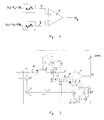
- FIG. 2 shows schematically the input and output of the differential amplifier and FIG. 3 shows the structure of a receiver for optical, spectrally coded Signals.
- FIG. 2 shows the two input signal branches of the differential amplifier 5.
- the upper signal branch A contains signal components which consist of the signal U 0 that is actually to be detected and an interference signal component U S and the test signal U e . These signal components undergo a phase delay ⁇ 1 in signal branch A with a change in amplitude of amplitude A 1 .
- the second signal branch B contains signal components from the interference signal U S , test signal U e and a somewhat different signal component ⁇ U 0 of the signal to be detected.
- the two signal branches are at the differently polarized inputs of the differential amplifier 5.
- the output signal is U a .
- the differences in the propagation factors A 1 and A 2 as well as ⁇ 1 and ⁇ 2 are to be measured and compensated for using appropriate control loops.
- the signal obtained from the above mixture of signal components is the output signal:
- U S denotes the interference signals to be suppressed, U 0 and ⁇ U 0 the signal to be received. If you only consider the additional test signal, the result is its amplitude
- test signal can be eliminated by suitable compensation of the amplitude difference and phase difference. If U e is corrected, the interference signals U S are also corrected, but not U 0 and ⁇ U 0 .
- FIG. 3 shows the above arrangement in a receiver EMP1, which is used for the detection of spectrally coded signals.
- the signal received by the EMP1 receiver consists of a large number of different spectra that are transmitted by different transmitters onto the transmission link. These spectrally coded individual channels are separated in the EMP1 receiver.
- the incoming signal passes through a coupler 11, which is connected to a light-emitting diode 6 and its control 7, realized with an HF current source.
- the signal passes through an optical isolator 12 and a further coupler 10, which divides the incoming signal.
- the incoming signal passes through an optical filter 2, a photodiode 4 and an amplifier 13 and is connected to the positive input of the differential amplifier 5.
- Signal branch A contains no other components.
- the divided signal component also passes through a photodiode 4, an amplifier 13, and in the signal branch B a transit time adjustment 8 and an amplitude adjustment 9, and is applied to the negative input of the differential amplifier.
- the output of the differential amplifier 5 delivers the output signal U a .
- the output of the differential amplifier 5 is connected to the input of an evaluation circuit 15, in which the output signal is broken down into an in-phase component I and a quadrature component Q.
- the I signal passes through a low-pass filter 6 and an integrator 16 of the amplitude adjustment 9.
- the signal of the amplitude adjustment 9 drives an adjustable amplifier 10.
- the Q signal passes through a low-pass filter 11, an integrator 12 and serves as a control signal for the phase setting 14.
- a setting component 3 for the rough phase position is connected to the evaluation circuit 15 and is used for the rough determination of the phase position.
- the evaluation circuit 15 can be implemented as a quadrature demodulator or as an IQ demodulator. It only requires a rough pre-setting of the phase position in order to be able to distinguish between the 1 and Q components, since the signal to be compensated does not have a fixed phase position.
- the fine tuning 17 of the optical filter 2 is also shown.
- the incoming optical spectrally coded signal first passes through the coupler 11, in which the test signal U e is injected.
- This test signal is generated by a light-emitting diode 6, which is operated at a frequency f 0 by the controller 7 (HF current source).
- the optical signal which is now expanded by the test signal U e , passes through the optical isolator 12, which prevents back-reflected signal components from being scattered back into the transmission network.
- the signals are separated into two signal branches. In an ideal case, the optical filter 2 should only let the desired signal U 0 into the signal branch A and suppress all interference.
- the detected test signal of the light-emitting diode 6 is measured after the differential amplifier via an evaluation circuit 15.
- the signal is set via the rough setting of the phase by the setting unit 3, the fine adjustment of the phase is carried out via the low-pass filter 14 and the integrator 12.
- the phase in the signal branch B is influenced by the phase setting 14.
- the signal is then amplified in the signal branch B, the degree of amplification being obtained from the I signal, which passes through the low-pass filter 9 and the integrator 16.
- the intervention on the transit times and signal levels can be done as in Embodiment electrical but also, as not explained in more detail, done optically. It is also possible in the upper arm of the recipient Fixed compensation elements for runtime and amplitude to provide.
- the modulation of the LED 6 can be sinusoidal, however, any other type of modulation, such as one Data modulation, permissible as long as the test signal from the signal mixture can be filtered out.
- the fine adjustment 17 of the optical filter 2 enables adjustment to different spectra of the spectrally coded signal. Thereby Separation of the channels is easily possible.
- the receiver contains a runtime adjustment and a Amplitude adjustment, the tuning of the control loop cause both signal branches.
- An amplifier (15) is also used, which is fed with the difference signal of the two signal branches. The This does not result in amplification through additional offsets or interference signals impaired. The regulation therefore allows optimal use of the Input dynamics of the amplifier.
- FIG. 4 Another embodiment of the invention is shown in FIG. 4 and explained in more detail in the following description.
- FIG 4 shows an arrangement in a receiver (EMP1) for Detection of spectrally coded signals is used.
- the signal from the Received (EMP1) consists of a variety of different spectra from different transmitters on the Transmission path are sent. This spectrally encoded individual Channels are separated in the receiver (EMP1).
- the incoming signal passes through a coupler 11, which with a LED 6 and its control 7, realized with an RF current source, connected is.
- the signal passes through an optical isolator 12 and one further coupler 10, which separates the incoming signal into two dividing signal branches A and B.
- the signal of signal branch A passes through an optical filter 2 and is replaced by a photodiode 10 changed.
- the now electrical signal is subject to one adjustable capacitance 130 and an adjustable resistor 120 and is via a resistor R and a summation point 160 with the input of amplifier 150 connected.
- the divided signal component likewise passes through a photodiode 110 and is connected to the summation point 100 and the amplifier 150 via a variable capacitance 130 ′ and an adjustable resistor 120 ′, analogously to the signal branch A.
- the phase and the amplitude of the two signal branches are regulated via a signal tap on the output side 30 of the amplifier 150.
- the resulting signal is taken off here.
- the output of the amplifier 150 is connected to the input of an evaluation circuit 140, in which the output signal is broken down into an in-phase component I and a quadrature component Q.
- the I signal controls the amplitude adjustment.
- the Q signal serves as a control signal for the phase adjustment.
- a setting component 3 for the rough phase position is connected to the evaluation circuit 140 and serves to roughly determine the phase position.
- the evaluation circuit 140 can be implemented as a quadrature demodulator or as an IQ demodulator. It only requires a rough pre-setting of the phase position in order to be able to distinguish between the 1 and Q components, since the signal to be compensated initially has no fixed phase position.
- the evaluation circuit 140 is connected on the output side to the variable components of the two signal branches.
- the photodiodes 100 and 110 are loaded with controllable complex impedances.
- Such a complex impedance is realized, for example, by a parallel connection of resistors and capacitors.
- the resistors can be realized by FETs, the capacitors by varactor diodes, so that an electrical adjustment of the resistance and capacitance values is possible.
- the rough setting is made in the upper branch.
- the lower branch B is connected to the evaluation unit 140, which enables fine tuning.
- the incoming optical spectrally coded signal first passes through the coupler 11, in which the test signal U e is injected.
- This test signal is generated by a light-emitting diode 6, which is operated at a frequency f 0 by the controller 7 (HF current source).
- the optical signal which is now expanded by the test signal U e , passes through the optical isolator 12, which prevents back-reflected signal components from being scattered back into the transmission network.
- the signals are separated into two signal branches. In an ideal case, the optical filter 2 should only let the desired signal U 0 into the signal branch A and suppress all interference.
- the test signal U e is divided into both signal branches. Both signal mixtures in both signal branches are converted into electrical signals by photodiodes 100, 110 and then amplified via an amplifier unit 150.
- the electrical signal in the lower signal branch B is loaded with a controllable, complex impedance and is present at the input of the amplifier 150.
- the transit time and the amplitude of the signal on the lower receiver arm can each be set via a control loop.
- the detected test signal of the light-emitting diode 6 is measured after the differential amplifier via an evaluation circuit 14.
- the signal is set via the rough setting of the phase by the setting unit 3, the fine adjustment of the phase is carried out via the IQ demodulator 140.
- the intervention on the transit times and signal levels can be done as in Embodiment electrical but also, as not explained in more detail, done optically. It is also possible in the upper arm of the recipient Fixed compensation elements for runtime and amplitude to provide.
- the modulation of the LED 6 can be sinusoidal, however, any other type of modulation, such as one Data modulation, permissible as long as the test signal from the signal mixture can be filtered out.
Landscapes
- Physics & Mathematics (AREA)
- Electromagnetism (AREA)
- Engineering & Computer Science (AREA)
- Computer Networks & Wireless Communication (AREA)
- Signal Processing (AREA)
- Optical Communication System (AREA)
Applications Claiming Priority (6)
| Application Number | Priority Date | Filing Date | Title |
|---|---|---|---|
| DE19723103 | 1997-06-03 | ||
| DE1997123103 DE19723103A1 (de) | 1997-06-03 | 1997-06-03 | Empfänger zum Empfang von optischen Signalen |
| DE19748756 | 1997-11-05 | ||
| DE1997148756 DE19748756A1 (de) | 1997-11-05 | 1997-11-05 | Empfänger für spektral kodierte optische Signale |
| DE1998109366 DE19809366A1 (de) | 1998-03-05 | 1998-03-05 | Empfänger für spektral kodierte optische Signale |
| DE19809366 | 1998-03-05 |
Publications (3)
| Publication Number | Publication Date |
|---|---|
| EP0883254A2 true EP0883254A2 (fr) | 1998-12-09 |
| EP0883254A3 EP0883254A3 (fr) | 2003-08-20 |
| EP0883254B1 EP0883254B1 (fr) | 2005-05-25 |
Family
ID=27217433
Family Applications (1)
| Application Number | Title | Priority Date | Filing Date |
|---|---|---|---|
| EP98440116A Expired - Lifetime EP0883254B1 (fr) | 1997-06-03 | 1998-06-02 | Récepteur pour réception de signaux optiques |
Country Status (5)
| Country | Link |
|---|---|
| US (1) | US6775484B1 (fr) |
| EP (1) | EP0883254B1 (fr) |
| JP (1) | JPH1174836A (fr) |
| CA (1) | CA2236862A1 (fr) |
| DE (1) | DE59812811D1 (fr) |
Cited By (2)
| Publication number | Priority date | Publication date | Assignee | Title |
|---|---|---|---|---|
| WO2005104406A1 (fr) * | 2004-04-22 | 2005-11-03 | Azea Networks Limited | Systeme de signalisation par boucle de renvoi pulsee a perte elevee |
| EP2543149A4 (fr) * | 2010-03-02 | 2014-05-28 | Onechip Photonics Inc | Affaiblissement diaphonique dans des émetteurs-récepteurs optiques |
Families Citing this family (4)
| Publication number | Priority date | Publication date | Assignee | Title |
|---|---|---|---|---|
| US7477852B2 (en) * | 2005-01-31 | 2009-01-13 | Alcatel-Lucent Usa Inc. | Optical receiver apparatus and method |
| JP5666617B2 (ja) * | 2010-03-17 | 2015-02-12 | ライトラボ・イメージング・インコーポレーテッド | 干渉センシングおよび画像取得システムのための強度雑音を低減する方法および装置 |
| US9337937B2 (en) | 2014-03-10 | 2016-05-10 | Cisco Technology, Inc. | Common mode rejection ratio control for coherent optical receivers |
| US10484089B1 (en) * | 2018-04-27 | 2019-11-19 | Hewlett Packard Enterprise Development Lp | Driver assisted by charge sharing |
Family Cites Families (20)
| Publication number | Priority date | Publication date | Assignee | Title |
|---|---|---|---|---|
| CH559990A5 (fr) | 1973-06-12 | 1975-03-14 | Patelhold Patentverwertung | |
| CH564889A5 (fr) | 1973-11-28 | 1975-07-31 | Patelhold Patentverwertung | |
| DE3011501C2 (de) | 1980-03-25 | 1994-01-20 | Siemens Ag | Optisches Kantenfilter |
| GB2121636B (en) | 1982-05-20 | 1986-03-05 | Standard Telephones Cables Ltd | Coherent optical receiver |
| DE3227682A1 (de) | 1982-07-24 | 1984-02-02 | Siemens Ag | Integrierte fotodioden als wellenlaengenselektive demultiplexeinrichtung |
| DE3840855C2 (de) | 1988-12-03 | 1996-07-18 | Telefunken Microelectron | Phasenvergleicher |
| US5115332A (en) | 1989-07-20 | 1992-05-19 | Fujitsu Limited | Receiver for coherent optical communication |
| US5081644A (en) | 1989-09-05 | 1992-01-14 | Clarion Co., Ltd. | Spread spectrum receiving device |
| JP2734778B2 (ja) * | 1991-01-16 | 1998-04-02 | 日本電気株式会社 | 光増幅装置 |
| DE4222208A1 (de) | 1992-07-07 | 1994-01-13 | Sel Alcatel Ag | Optisches Nachrichtenübertragungssystem mit optischem Filter zum Schutz vor Riesenimpulsen |
| US5483368A (en) * | 1992-11-18 | 1996-01-09 | Kabushiki Kaisha Toshiba | Optical communication system suitable for selective reception of multiple services |
| GB2274952B (en) * | 1993-01-23 | 1996-12-04 | Northern Telecom Ltd | Optical soliton pulse transmission system |
| FR2708753B1 (fr) * | 1993-07-30 | 1995-09-01 | Cit Alcatel | Dispositif d'accord de filtre optique accordable utilisable notamment en réception dans un système de transmission optique. |
| DE4403985A1 (de) | 1994-02-07 | 1995-08-10 | Nokia Deutschland Gmbh | Schaltungsanordnung für einen Lichtsignalempfänger |
| JP3303515B2 (ja) * | 1994-03-18 | 2002-07-22 | キヤノン株式会社 | 光通信方式及びそれを用いた光通信システム |
| IT1277397B1 (it) * | 1995-07-31 | 1997-11-10 | Pirelli Cavi S P A Ora Pirelli | Sistema e metodo di telecomunicazione a multiplazione di lunghezza d'onda con separazione controllata dei canali in uscita |
| JP3272934B2 (ja) | 1996-02-07 | 2002-04-08 | 安藤電気株式会社 | 波長多重光増幅器の評価測定装置および方法 |
| DE19605567A1 (de) | 1996-02-15 | 1997-08-21 | Sel Alcatel Ag | Optisches frequenzkodiertes CDMA-Übertragungssystem und optischer Empfänger dafür |
| DE19612604A1 (de) | 1996-03-29 | 1997-10-02 | Sel Alcatel Ag | Optischer Empfänger mit einer Entzerrerschaltung für durch PMD verursachte Störungen und System mit einem solchen optischen Empfänger |
| JPH1051388A (ja) * | 1996-08-01 | 1998-02-20 | Nec Corp | 光増幅装置 |
-
1998
- 1998-05-28 US US09/086,026 patent/US6775484B1/en not_active Expired - Fee Related
- 1998-06-02 CA CA002236862A patent/CA2236862A1/fr not_active Abandoned
- 1998-06-02 DE DE59812811T patent/DE59812811D1/de not_active Expired - Fee Related
- 1998-06-02 EP EP98440116A patent/EP0883254B1/fr not_active Expired - Lifetime
- 1998-06-03 JP JP10154968A patent/JPH1174836A/ja active Pending
Cited By (3)
| Publication number | Priority date | Publication date | Assignee | Title |
|---|---|---|---|---|
| WO2005104406A1 (fr) * | 2004-04-22 | 2005-11-03 | Azea Networks Limited | Systeme de signalisation par boucle de renvoi pulsee a perte elevee |
| US7684711B2 (en) | 2004-04-22 | 2010-03-23 | Xtera Communications, Inc. | Pulsed high loss loop back signalling scheme |
| EP2543149A4 (fr) * | 2010-03-02 | 2014-05-28 | Onechip Photonics Inc | Affaiblissement diaphonique dans des émetteurs-récepteurs optiques |
Also Published As
| Publication number | Publication date |
|---|---|
| CA2236862A1 (fr) | 1998-12-03 |
| DE59812811D1 (de) | 2005-06-30 |
| EP0883254A3 (fr) | 2003-08-20 |
| JPH1174836A (ja) | 1999-03-16 |
| EP0883254B1 (fr) | 2005-05-25 |
| US6775484B1 (en) | 2004-08-10 |
Similar Documents
| Publication | Publication Date | Title |
|---|---|---|
| DE60034618T2 (de) | Optischer Verstärker zur Verschiebung der Ramanverstärkung angeordnet | |
| DE3232430C2 (de) | Optisches Nachrichtenübertragungssystem | |
| DE60027123T2 (de) | Schaltung zur Komprimierung des dynamischen Bereich eines Signals | |
| DE3782556T2 (de) | Lichtuebertragungssystem. | |
| DE60119573T2 (de) | Vorrichtung und verfahren zur unterdrückung des relativen intensitätsrauschens und verbesserung des sendersignals in einem optischen übertragungssystem | |
| DE68922412T2 (de) | Optischer Sender, optischer Empfänger und optische Übertragungsvorrichtung sowie Regelungsverfahren für optischen Empfänger. | |
| DE69124301T2 (de) | Demodulator und Polarisationsdiversitätempfänger für kohärente optische Übertragung mit dem Demodulator | |
| DE69128537T2 (de) | Optisches Übertragungssystem | |
| DE69624680T2 (de) | AM/FM Umsetzer und Lichtwellensignalübertragungssystem | |
| DE19722370A1 (de) | Empfänger für ein optisches Nachrichtenübertragungssystem und Verfahren zu dessen Betrieb | |
| EP1026849A2 (fr) | Système de transmission optique ainsi qu'émetteur et récepteur | |
| DE3853969T2 (de) | Optisches Gerät zum Ziehen einer Zwischenfrequenz in einen bestimmten Frequenzbereich. | |
| DE60126542T2 (de) | Optisches Übertragungssystem und optischer Empfänger | |
| EP0883254A2 (fr) | Récepteur pour réception de signaux optiques | |
| DE69902759T2 (de) | Optische verbindungen | |
| DE3106450A1 (de) | Laser-digitalsender | |
| DE69832560T2 (de) | FM-Modulator | |
| EP0417148A1 (fr) | Element de reception radio fm. | |
| DE10216281B4 (de) | Anordnung und Verfahren für eine Dispersionsdetektion | |
| EP0417149A1 (fr) | Element de reception radio fm. | |
| WO1989012353A1 (fr) | Element de reception fm | |
| EP0418270A1 (fr) | Element de reception radio fm. | |
| EP0280075B1 (fr) | Récepteur optique à diversité de polarisation | |
| DE60028517T2 (de) | Verfahren zur Initialisierung eines optischen Senders | |
| EP0298484B1 (fr) | Récepteur optique synchrone pour signaux FSK |
Legal Events
| Date | Code | Title | Description |
|---|---|---|---|
| PUAI | Public reference made under article 153(3) epc to a published international application that has entered the european phase |
Free format text: ORIGINAL CODE: 0009012 |
|
| AK | Designated contracting states |
Kind code of ref document: A2 Designated state(s): AT BE CH CY DE DK ES FI FR GB GR IE IT LI LU MC NL PT SE |
|
| AX | Request for extension of the european patent |
Free format text: AL;LT;LV;MK;RO;SI |
|
| RAP3 | Party data changed (applicant data changed or rights of an application transferred) |
Owner name: ALCATEL |
|
| 17P | Request for examination filed |
Effective date: 20010310 |
|
| PUAL | Search report despatched |
Free format text: ORIGINAL CODE: 0009013 |
|
| AK | Designated contracting states |
Designated state(s): AT BE CH CY DE DK ES FI FR GB GR IE IT LI LU MC NL PT SE |
|
| AX | Request for extension of the european patent |
Extension state: AL LT LV MK RO SI |
|
| 17Q | First examination report despatched |
Effective date: 20031104 |
|
| AKX | Designation fees paid |
Designated state(s): DE FI FR GB IT SE |
|
| GRAP | Despatch of communication of intention to grant a patent |
Free format text: ORIGINAL CODE: EPIDOSNIGR1 |
|
| GRAS | Grant fee paid |
Free format text: ORIGINAL CODE: EPIDOSNIGR3 |
|
| GRAA | (expected) grant |
Free format text: ORIGINAL CODE: 0009210 |
|
| AK | Designated contracting states |
Kind code of ref document: B1 Designated state(s): DE FI FR GB IT SE |
|
| PG25 | Lapsed in a contracting state [announced via postgrant information from national office to epo] |
Ref country code: IT Free format text: LAPSE BECAUSE OF FAILURE TO SUBMIT A TRANSLATION OF THE DESCRIPTION OR TO PAY THE FEE WITHIN THE PRESCRIBED TIME-LIMIT;WARNING: LAPSES OF ITALIAN PATENTS WITH EFFECTIVE DATE BEFORE 2007 MAY HAVE OCCURRED AT ANY TIME BEFORE 2007. THE CORRECT EFFECTIVE DATE MAY BE DIFFERENT FROM THE ONE RECORDED. Effective date: 20050525 Ref country code: FI Free format text: LAPSE BECAUSE OF FAILURE TO SUBMIT A TRANSLATION OF THE DESCRIPTION OR TO PAY THE FEE WITHIN THE PRESCRIBED TIME-LIMIT Effective date: 20050525 |
|
| REG | Reference to a national code |
Ref country code: GB Ref legal event code: FG4D Free format text: NOT ENGLISH |
|
| GBT | Gb: translation of ep patent filed (gb section 77(6)(a)/1977) |
Effective date: 20050525 |
|
| REG | Reference to a national code |
Ref country code: IE Ref legal event code: FG4D Free format text: LANGUAGE OF EP DOCUMENT: GERMAN |
|
| REF | Corresponds to: |
Ref document number: 59812811 Country of ref document: DE Date of ref document: 20050630 Kind code of ref document: P |
|
| PG25 | Lapsed in a contracting state [announced via postgrant information from national office to epo] |
Ref country code: SE Free format text: LAPSE BECAUSE OF FAILURE TO SUBMIT A TRANSLATION OF THE DESCRIPTION OR TO PAY THE FEE WITHIN THE PRESCRIBED TIME-LIMIT Effective date: 20050825 |
|
| ET | Fr: translation filed | ||
| PLBE | No opposition filed within time limit |
Free format text: ORIGINAL CODE: 0009261 |
|
| STAA | Information on the status of an ep patent application or granted ep patent |
Free format text: STATUS: NO OPPOSITION FILED WITHIN TIME LIMIT |
|
| 26N | No opposition filed |
Effective date: 20060228 |
|
| PGFP | Annual fee paid to national office [announced via postgrant information from national office to epo] |
Ref country code: DE Payment date: 20070622 Year of fee payment: 10 |
|
| PGFP | Annual fee paid to national office [announced via postgrant information from national office to epo] |
Ref country code: GB Payment date: 20070621 Year of fee payment: 10 |
|
| PGFP | Annual fee paid to national office [announced via postgrant information from national office to epo] |
Ref country code: FR Payment date: 20070615 Year of fee payment: 10 |
|
| GBPC | Gb: european patent ceased through non-payment of renewal fee |
Effective date: 20080602 |
|
| REG | Reference to a national code |
Ref country code: FR Ref legal event code: ST Effective date: 20090228 |
|
| PG25 | Lapsed in a contracting state [announced via postgrant information from national office to epo] |
Ref country code: DE Free format text: LAPSE BECAUSE OF NON-PAYMENT OF DUE FEES Effective date: 20090101 |
|
| PG25 | Lapsed in a contracting state [announced via postgrant information from national office to epo] |
Ref country code: GB Free format text: LAPSE BECAUSE OF NON-PAYMENT OF DUE FEES Effective date: 20080602 |
|
| PG25 | Lapsed in a contracting state [announced via postgrant information from national office to epo] |
Ref country code: FR Free format text: LAPSE BECAUSE OF NON-PAYMENT OF DUE FEES Effective date: 20080630 |