EP0883268A1 - Verfahren und Einrichtung zur Schätzung der Frequenzverschiebungen eines von einem Mobiltelefondemodulator empfangenen Signals - Google Patents
Verfahren und Einrichtung zur Schätzung der Frequenzverschiebungen eines von einem Mobiltelefondemodulator empfangenen Signals Download PDFInfo
- Publication number
- EP0883268A1 EP0883268A1 EP98401323A EP98401323A EP0883268A1 EP 0883268 A1 EP0883268 A1 EP 0883268A1 EP 98401323 A EP98401323 A EP 98401323A EP 98401323 A EP98401323 A EP 98401323A EP 0883268 A1 EP0883268 A1 EP 0883268A1
- Authority
- EP
- European Patent Office
- Prior art keywords
- raw
- signal
- phase
- estimate
- demodulator
- Prior art date
- Legal status (The legal status is an assumption and is not a legal conclusion. Google has not performed a legal analysis and makes no representation as to the accuracy of the status listed.)
- Granted
Links
- 238000000034 method Methods 0.000 title claims description 10
- 230000006870 function Effects 0.000 claims description 13
- 239000000523 sample Substances 0.000 description 8
- 238000010586 diagram Methods 0.000 description 7
- 230000000694 effects Effects 0.000 description 4
- 238000004364 calculation method Methods 0.000 description 2
- 230000001427 coherent effect Effects 0.000 description 2
- 239000000654 additive Substances 0.000 description 1
- 230000000996 additive effect Effects 0.000 description 1
- 230000009286 beneficial effect Effects 0.000 description 1
- 238000004422 calculation algorithm Methods 0.000 description 1
- 230000002349 favourable effect Effects 0.000 description 1
- 238000005070 sampling Methods 0.000 description 1
- 238000004088 simulation Methods 0.000 description 1
Images


Classifications
-
- H—ELECTRICITY
- H04—ELECTRIC COMMUNICATION TECHNIQUE
- H04L—TRANSMISSION OF DIGITAL INFORMATION, e.g. TELEGRAPHIC COMMUNICATION
- H04L27/00—Modulated-carrier systems
- H04L27/18—Phase-modulated carrier systems, i.e. using phase-shift keying
- H04L27/22—Demodulator circuits; Receiver circuits
- H04L27/227—Demodulator circuits; Receiver circuits using coherent demodulation
- H04L27/2271—Demodulator circuits; Receiver circuits using coherent demodulation wherein the carrier recovery circuit uses only the demodulated signals
- H04L27/2273—Demodulator circuits; Receiver circuits using coherent demodulation wherein the carrier recovery circuit uses only the demodulated signals associated with quadrature demodulation, e.g. Costas loop
-
- H—ELECTRICITY
- H04—ELECTRIC COMMUNICATION TECHNIQUE
- H04L—TRANSMISSION OF DIGITAL INFORMATION, e.g. TELEGRAPHIC COMMUNICATION
- H04L27/00—Modulated-carrier systems
- H04L27/18—Phase-modulated carrier systems, i.e. using phase-shift keying
- H04L27/22—Demodulator circuits; Receiver circuits
- H04L27/233—Demodulator circuits; Receiver circuits using non-coherent demodulation
- H04L27/2332—Demodulator circuits; Receiver circuits using non-coherent demodulation using a non-coherent carrier
-
- H—ELECTRICITY
- H04—ELECTRIC COMMUNICATION TECHNIQUE
- H04L—TRANSMISSION OF DIGITAL INFORMATION, e.g. TELEGRAPHIC COMMUNICATION
- H04L27/00—Modulated-carrier systems
- H04L27/0014—Carrier regulation
- H04L2027/0044—Control loops for carrier regulation
- H04L2027/0063—Elements of loops
- H04L2027/0065—Frequency error detectors
Definitions
- the present invention relates to a device for estimating the frequency offset, in particular for a mobile-telephone demodulator.
- Frequency modulation is the modulation technique most widely used in mobile radio systems.
- the signals In frequency modulation, the signals have all their information contained in the phase or the frequency of the carrier.
- the demodulator which is used In order to recover the data, the demodulator which is used must estimate the phase or the frequency of the signal. If the carrier frequency is not exactly the expected frequency (because of a difference in frequency between the frequency of the oscillators of the transmitter and of the receiver), this may lead to an inaccuracy, and therefore increase the error rate of the demodulator.
- One of the great problems with radio systems is that of reducing the impact of the frequency error of the received signal by compensating for it locally.
- the receiver successively receives signals from different transmitters, it must frequently estimate new frequency errors.
- the frequency error estimator must give a reliable estimate on the basis of a very small number of samples.
- the object of the invention is to create a very efficient frequency error estimator used with a differential phase demodulator.
- a further object of the invention is to create a frequency error estimator which is particularly well-suited to a ⁇ /4 QPSK demodulator, having four-state phase modulation with a jump of ⁇ /4, dedicated to wireless applications such as PHS and PDC mobile telephones.
- the invention therefore relates to a method for estimating the frequency offset in a signal received by a demodulator of a mobile-telephone set.
- the method includes the steps of :
- ⁇ (kT) generally belongs to a certain group of possible values.
- Figure 1 shows four QPSK modulation phase points.
- the first expression X is filtered in the demodulator.
- the second expression Z contains the information.
- the first expression X is filtered in the demodulator.
- the second expression Z contains the information.
- This phase error can be corrected easily.
- the role of the frequency offset error estimator is to give an estimate of ⁇ e as quickly as possible and with the best reliability, even in a highly unfavourable environment.
- a normal demodulator calculates the in-phase and quadrature components I and Q of the signal in order to recover the data.
- the example will be taken of ⁇ /4 QPSK modulation used in PHS, PDC, PACS systems, for example.
- the frequency offset estimator uses the error between the sample (white dot in Figure 2) and the ideal sample (grey dot).
- This error is referred to as ⁇ .
- the error is - ⁇ .
- Figure 5 shows the histogram of the in-phase component I in a noisy environment and without frequency error.
- the error estimate is ⁇ 2.
- Figure 6 shows the histogram of I in a noisy environment with a frequency error.
- the error on FO-RAW increases with the frequency error and the amount of noise.
- FO-RAW FO-RAW (frequency offset, quality)
- the estimate Q-RAW is bound to increase with the frequency offset.
- Q-RAW delivers a high value even if the quality of the signal is very good.
- Figure 7 shows the impact of the frequency offset on the quality estimate.
- Q-RAW Q-RAW (frequency offset, quality).
- the frequency offset information contained both in the signals FO-RAW and Q-RAW is used, and the quality information is removed.
- ⁇ is made by using a ROM memory.
- the ROM memory may, of course, be synthesized by combinatorial logic in order to obtain a more efficient embodiment.
- ⁇ may be calculated directly using system equations.
- the coefficients could be calculated by simulation or by experimentation.
- ⁇ n be the frequency error during test number n.
- FO-RAW n and Q-RAW n be the corresponding values of FO-RAW and Q-RAW.
- the demodulator provides the frequency offset estimator with an estimate of the in-phase and quadrature components I and Q of the signal which it has received.
- the error ⁇ on I is then estimated and corrected in order to remove the variation in sign according to the value Q of the sample, as indicated at the start of the description.
- the estimates FO-RAW and Q-RAW are calculated over the amount of samples available.
- n FO-RAW and n Q-RAW are respectively the number of bits used in FO-RAW and Q-RAW.
- n freq.offset is the number of bits in the estimate of the frequency offset.
- ROM dimension 2 (n FO-RAW + n Q-RAW )*n freq.offset
- the ROM memory may be replaced by a logic circuit.
- the dimension of the embodiment may be improved considerably by virtue of the redundancy and the symmetry in ⁇ .
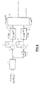
- It comprises an error calculation circuit 1 which, on its inputs, receives the signals I, Q drawn from the transmitted signal and I o , Q o corresponding to the ideal phase.
- the circuit 1 is connected at its output to a first adder 2 directly and to a second adder 3 via a circuit 4 for establishing the absolute value ABS of the error signal ⁇ appearing at the output of the error calculation circuit 1.
- the output of the first adder 2 is connected to an FO-RAW circuit 5 intended to take n FO-RAW bits from the available FO-RAW bits.
- the output of the second adder 3 is connected to the input of a Q-RAW circuit 6 intended to take n Q-RAW bits from the available Q-RAW bits.
- the outputs of the first and second adders 2 and 3 are furthermore looped back onto the second inputs via respective one-symbol delay circuits 7, 8.
- the outputs of the circuits 5 and 6 are connected to corresponding address inputs of a ROM memory 10 which is programmed in the manner indicated above and which constitutes means for modelling the function ⁇ (FO-RAW, Q-RAW).
- the frequency offset signal appears at the output of this ROM memory.
- the application range is -9 ppm to 9 ppm.
- the algorithm firstly estimates the average of the phase error of the demodulated signal and its variance.
- the efficiency of the method and of the device of the invention makes it possible to correct the frequency within a packet, and not to wait for the next data packet in order to apply the estimate.
- This characteristic is highly beneficial in the case of demodulating a plurality of base stations which have different frequency offsets.
Landscapes
- Engineering & Computer Science (AREA)
- Computer Networks & Wireless Communication (AREA)
- Signal Processing (AREA)
- Digital Transmission Methods That Use Modulated Carrier Waves (AREA)
Applications Claiming Priority (3)
| Application Number | Priority Date | Filing Date | Title |
|---|---|---|---|
| FR9706810 | 1997-06-03 | ||
| FR9706810A FR2764158B1 (fr) | 1997-06-03 | 1997-06-03 | Procede et dispositif d'estimation du decalage de frequence dans un signal recu par un demodulateur de telephone mobile |
| US09/089,791 US6449470B1 (en) | 1997-06-03 | 1998-06-03 | Method and device for estimating the frequency offset in a signal received by a mobile-telephone demodulator |
Publications (2)
| Publication Number | Publication Date |
|---|---|
| EP0883268A1 true EP0883268A1 (de) | 1998-12-09 |
| EP0883268B1 EP0883268B1 (de) | 2005-08-17 |
Family
ID=26233579
Family Applications (1)
| Application Number | Title | Priority Date | Filing Date |
|---|---|---|---|
| EP98401323A Expired - Lifetime EP0883268B1 (de) | 1997-06-03 | 1998-06-03 | Verfahren und Einrichtung zur Schätzung der Frequenzverschiebungen eines von einem Mobiltelefondemodulator empfangenen Signals |
Country Status (3)
| Country | Link |
|---|---|
| US (1) | US6449470B1 (de) |
| EP (1) | EP0883268B1 (de) |
| FR (1) | FR2764158B1 (de) |
Citations (4)
| Publication number | Priority date | Publication date | Assignee | Title |
|---|---|---|---|---|
| EP0108358A2 (de) * | 1982-10-30 | 1984-05-16 | Nec Corporation | Phasendemodulator |
| EP0252500A2 (de) * | 1986-07-09 | 1988-01-13 | Nec Corporation | Demodulator für 8-stufige Phasenumtastung |
| EP0533208A2 (de) * | 1991-09-19 | 1993-03-24 | Nec Corporation | PSK-Demodulator mit Rückkopplungsschaltung zur Phasen- und Frequenzkorrektur |
| EP0564361A1 (de) * | 1992-04-03 | 1993-10-06 | Alcatel Telspace | Einrichtung zur Demodulation von pi/4-QPSK-Signalen |
Family Cites Families (8)
| Publication number | Priority date | Publication date | Assignee | Title |
|---|---|---|---|---|
| US4633485A (en) * | 1985-03-08 | 1986-12-30 | Paradyne Corporation | Adaptive noise suppression for digital modems |
| US4669090A (en) * | 1985-07-05 | 1987-05-26 | Paradyne Corporation | Half-duplex modem without turnaround delay |
| US4963839A (en) * | 1989-09-01 | 1990-10-16 | Westinghouse Electric Corp. | Wide bandwidth phase locked loop circuit with sliding window averager |
| US5060180A (en) * | 1990-07-26 | 1991-10-22 | Unisys Corporation | Programmable digital loop filter |
| US5452327A (en) * | 1993-12-28 | 1995-09-19 | Unisys Corporation | Programmable randomly tunable digital demodulator |
| JP3596827B2 (ja) * | 1995-07-06 | 2004-12-02 | パイオニア株式会社 | ディジタルpll回路 |
| US5646968A (en) * | 1995-11-17 | 1997-07-08 | Analog Devices, Inc. | Dynamic phase selector phase locked loop circuit |
| EP0782271B1 (de) * | 1995-12-28 | 2002-03-13 | Thomson Consumer Electronics, Inc. | Phasenregelschleife mit regelbarer Antwortzeit |
-
1997
- 1997-06-03 FR FR9706810A patent/FR2764158B1/fr not_active Expired - Fee Related
-
1998
- 1998-06-03 EP EP98401323A patent/EP0883268B1/de not_active Expired - Lifetime
- 1998-06-03 US US09/089,791 patent/US6449470B1/en not_active Expired - Lifetime
Patent Citations (4)
| Publication number | Priority date | Publication date | Assignee | Title |
|---|---|---|---|---|
| EP0108358A2 (de) * | 1982-10-30 | 1984-05-16 | Nec Corporation | Phasendemodulator |
| EP0252500A2 (de) * | 1986-07-09 | 1988-01-13 | Nec Corporation | Demodulator für 8-stufige Phasenumtastung |
| EP0533208A2 (de) * | 1991-09-19 | 1993-03-24 | Nec Corporation | PSK-Demodulator mit Rückkopplungsschaltung zur Phasen- und Frequenzkorrektur |
| EP0564361A1 (de) * | 1992-04-03 | 1993-10-06 | Alcatel Telspace | Einrichtung zur Demodulation von pi/4-QPSK-Signalen |
Non-Patent Citations (2)
| Title |
|---|
| FINES, AGHVAMI: "A comparison study of low bit rate DE-QPSK and TCM 8-PSK fully digital demodulators over a land mobile satellite link", IEEE GLOBAL TELECOMMUNICATIONS CONFERENCE 1990, 2 December 1990 (1990-12-02) - 5 December 1990 (1990-12-05), NEW YORK, US, pages 387 - 392, XP000218759 * |
| MATSUMOTO ET AL.: "VLSI implemented 60 Mb/s QPSK/OQPSK burst digital demodulator for radio application", IEICE TRANSACTIONS ON ELECTRONICS., vol. E77-C, no. 12, December 1994 (1994-12-01), TOKYO, JP, pages 1873 - 1880, XP000497018 * |
Also Published As
| Publication number | Publication date |
|---|---|
| EP0883268B1 (de) | 2005-08-17 |
| US6449470B1 (en) | 2002-09-10 |
| FR2764158A1 (fr) | 1998-12-04 |
| FR2764158B1 (fr) | 1999-08-20 |
Similar Documents
| Publication | Publication Date | Title |
|---|---|---|
| US7016404B2 (en) | Automatic frequency correction for mobile radio receivers | |
| US6628926B1 (en) | Method for automatic frequency control | |
| CN1595919B (zh) | 补偿传输信道随时间的频移及相位改变之方法及接收单元 | |
| WO2001020863A1 (en) | Method and apparatus for carrier phase tracking | |
| US20040180635A1 (en) | Apparatus and method for compensating for frequency offset in a mobile communication system | |
| US5195108A (en) | System and method for determining absolute phase of a differentially-encoded, phase-modulated signal | |
| US6603821B1 (en) | Wireless communication terminal capable of correctly specifying position of burst and having small frequency error of recovered carrier | |
| US6546026B1 (en) | Multi-diversity synchronization technique for improving synchronization performance in wireless applications over fading channels | |
| US6442218B1 (en) | Demodulator | |
| JPH07297870A (ja) | Tdmaデータ受信装置 | |
| US6625237B2 (en) | Null-pilot symbol assisted fast automatic frequency control (AFC) system for coherent demodulation of continuous phase modulation (CPM) signals and method for implementing same | |
| AU723965B2 (en) | Channel estimation arrangement | |
| US6449470B1 (en) | Method and device for estimating the frequency offset in a signal received by a mobile-telephone demodulator | |
| CN101646232B (zh) | 频偏估计方法、装置以及通信设备 | |
| US6044119A (en) | Frequency control method and circuit employing both reference symbols and information symbols | |
| US6859507B2 (en) | Method and apparatus for correcting a signal | |
| US6603820B1 (en) | Demodulator having rotation means for frequency offset correction | |
| KR101019171B1 (ko) | 재변조를 이용한 주파수 에러 정정 | |
| CN116346209A (zh) | 一种mpsk卫星通信系统载波同步方法 | |
| EP1313279A1 (de) | Verfahren zur Korrektur von Phasenverschiebungen in einem Signal und entsprechender Empfänger | |
| US7388902B2 (en) | Method for receiving spectrum spreading signals with frequency shift correction | |
| US6587523B1 (en) | Radio signal receiving apparatus and a method of radio signal reception | |
| EP2068521B1 (de) | QAM-Phasenfehlerdetektor | |
| US7164733B1 (en) | Method and device for compensating for digital data demodulation phase uncertainty | |
| EP1313280A1 (de) | Verfahren zur Korrektur von Phasenfehlern in einem empfangenen Signal sowie entsprechender Empfänger |
Legal Events
| Date | Code | Title | Description |
|---|---|---|---|
| PUAI | Public reference made under article 153(3) epc to a published international application that has entered the european phase |
Free format text: ORIGINAL CODE: 0009012 |
|
| AK | Designated contracting states |
Kind code of ref document: A1 Designated state(s): DE FR GB IT NL |
|
| AX | Request for extension of the european patent |
Free format text: AL;LT;LV;MK;RO;SI |
|
| 17P | Request for examination filed |
Effective date: 19990213 |
|
| AKX | Designation fees paid |
Free format text: DE FR GB IT NL |
|
| 17Q | First examination report despatched |
Effective date: 20040210 |
|
| GRAP | Despatch of communication of intention to grant a patent |
Free format text: ORIGINAL CODE: EPIDOSNIGR1 |
|
| RAP1 | Party data changed (applicant data changed or rights of an application transferred) |
Owner name: TEXAS INSTRUMENTS INCORPORATED Owner name: TEXAS INSTRUMENTS FRANCE |
|
| GRAS | Grant fee paid |
Free format text: ORIGINAL CODE: EPIDOSNIGR3 |
|
| GRAA | (expected) grant |
Free format text: ORIGINAL CODE: 0009210 |
|
| AK | Designated contracting states |
Kind code of ref document: B1 Designated state(s): DE FR GB IT NL |
|
| PG25 | Lapsed in a contracting state [announced via postgrant information from national office to epo] |
Ref country code: NL Free format text: LAPSE BECAUSE OF FAILURE TO SUBMIT A TRANSLATION OF THE DESCRIPTION OR TO PAY THE FEE WITHIN THE PRESCRIBED TIME-LIMIT Effective date: 20050817 Ref country code: IT Free format text: LAPSE BECAUSE OF FAILURE TO SUBMIT A TRANSLATION OF THE DESCRIPTION OR TO PAY THE FEE WITHIN THE PRESCRIBED TIME-LIMIT;WARNING: LAPSES OF ITALIAN PATENTS WITH EFFECTIVE DATE BEFORE 2007 MAY HAVE OCCURRED AT ANY TIME BEFORE 2007. THE CORRECT EFFECTIVE DATE MAY BE DIFFERENT FROM THE ONE RECORDED. Effective date: 20050817 |
|
| REG | Reference to a national code |
Ref country code: GB Ref legal event code: FG4D |
|
| REF | Corresponds to: |
Ref document number: 69831190 Country of ref document: DE Date of ref document: 20050922 Kind code of ref document: P |
|
| NLV1 | Nl: lapsed or annulled due to failure to fulfill the requirements of art. 29p and 29m of the patents act | ||
| ET | Fr: translation filed | ||
| PLBE | No opposition filed within time limit |
Free format text: ORIGINAL CODE: 0009261 |
|
| STAA | Information on the status of an ep patent application or granted ep patent |
Free format text: STATUS: NO OPPOSITION FILED WITHIN TIME LIMIT |
|
| 26N | No opposition filed |
Effective date: 20060518 |
|
| PGFP | Annual fee paid to national office [announced via postgrant information from national office to epo] |
Ref country code: DE Payment date: 20090630 Year of fee payment: 12 |
|
| PG25 | Lapsed in a contracting state [announced via postgrant information from national office to epo] |
Ref country code: DE Free format text: LAPSE BECAUSE OF NON-PAYMENT OF DUE FEES Effective date: 20110101 |
|
| PGFP | Annual fee paid to national office [announced via postgrant information from national office to epo] |
Ref country code: FR Payment date: 20130618 Year of fee payment: 16 |
|
| PGFP | Annual fee paid to national office [announced via postgrant information from national office to epo] |
Ref country code: GB Payment date: 20140527 Year of fee payment: 17 |
|
| REG | Reference to a national code |
Ref country code: FR Ref legal event code: ST Effective date: 20150227 |
|
| PG25 | Lapsed in a contracting state [announced via postgrant information from national office to epo] |
Ref country code: FR Free format text: LAPSE BECAUSE OF NON-PAYMENT OF DUE FEES Effective date: 20140630 |
|
| GBPC | Gb: european patent ceased through non-payment of renewal fee |
Effective date: 20150603 |
|
| PG25 | Lapsed in a contracting state [announced via postgrant information from national office to epo] |
Ref country code: GB Free format text: LAPSE BECAUSE OF NON-PAYMENT OF DUE FEES Effective date: 20150603 |