EP0884716A2 - Système d'affichage adressé par plasma - Google Patents
Système d'affichage adressé par plasma Download PDFInfo
- Publication number
- EP0884716A2 EP0884716A2 EP98110551A EP98110551A EP0884716A2 EP 0884716 A2 EP0884716 A2 EP 0884716A2 EP 98110551 A EP98110551 A EP 98110551A EP 98110551 A EP98110551 A EP 98110551A EP 0884716 A2 EP0884716 A2 EP 0884716A2
- Authority
- EP
- European Patent Office
- Prior art keywords
- pixels
- row
- plasma
- discharge
- display system
- Prior art date
- Legal status (The legal status is an assumption and is not a legal conclusion. Google has not performed a legal analysis and makes no representation as to the accuracy of the status listed.)
- Granted
Links
Images


Classifications
-
- G—PHYSICS
- G02—OPTICS
- G02F—OPTICAL DEVICES OR ARRANGEMENTS FOR THE CONTROL OF LIGHT BY MODIFICATION OF THE OPTICAL PROPERTIES OF THE MEDIA OF THE ELEMENTS INVOLVED THEREIN; NON-LINEAR OPTICS; FREQUENCY-CHANGING OF LIGHT; OPTICAL LOGIC ELEMENTS; OPTICAL ANALOGUE/DIGITAL CONVERTERS
- G02F1/00—Devices or arrangements for the control of the intensity, colour, phase, polarisation or direction of light arriving from an independent light source, e.g. switching, gating or modulating; Non-linear optics
- G02F1/01—Devices or arrangements for the control of the intensity, colour, phase, polarisation or direction of light arriving from an independent light source, e.g. switching, gating or modulating; Non-linear optics for the control of the intensity, phase, polarisation or colour
- G02F1/13—Devices or arrangements for the control of the intensity, colour, phase, polarisation or direction of light arriving from an independent light source, e.g. switching, gating or modulating; Non-linear optics for the control of the intensity, phase, polarisation or colour based on liquid crystals, e.g. single liquid crystal display cells
- G02F1/133—Constructional arrangements; Operation of liquid crystal cells; Circuit arrangements
- G02F1/1333—Constructional arrangements; Manufacturing methods
- G02F1/13334—Plasma addressed liquid crystal cells [PALC]
-
- G—PHYSICS
- G09—EDUCATION; CRYPTOGRAPHY; DISPLAY; ADVERTISING; SEALS
- G09G—ARRANGEMENTS OR CIRCUITS FOR CONTROL OF INDICATING DEVICES USING STATIC MEANS TO PRESENT VARIABLE INFORMATION
- G09G3/00—Control arrangements or circuits, of interest only in connection with visual indicators other than cathode-ray tubes
- G09G3/20—Control arrangements or circuits, of interest only in connection with visual indicators other than cathode-ray tubes for presentation of an assembly of a number of characters, e.g. a page, by composing the assembly by combination of individual elements arranged in a matrix no fixed position being assigned to or needed to be assigned to the individual characters or partial characters
- G09G3/34—Control arrangements or circuits, of interest only in connection with visual indicators other than cathode-ray tubes for presentation of an assembly of a number of characters, e.g. a page, by composing the assembly by combination of individual elements arranged in a matrix no fixed position being assigned to or needed to be assigned to the individual characters or partial characters by control of light from an independent source
- G09G3/36—Control arrangements or circuits, of interest only in connection with visual indicators other than cathode-ray tubes for presentation of an assembly of a number of characters, e.g. a page, by composing the assembly by combination of individual elements arranged in a matrix no fixed position being assigned to or needed to be assigned to the individual characters or partial characters by control of light from an independent source using liquid crystals
- G09G3/3611—Control of matrices with row and column drivers
- G09G3/3648—Control of matrices with row and column drivers using an active matrix
- G09G3/3662—Control of matrices with row and column drivers using an active matrix using plasma-addressed liquid crystal displays
Definitions
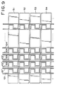
- An image processing circuit 28 is connected to the signal circuit 23 and serves to convert a primary image signal, which is supplied from an external apparatus, into a secondary image signal adapted for driving the panel 0. More concretely, the image processing circuit 28 first performs two-dimensional filtering of a primary image signal for applying the same to a predetermined mask pattern, and then supplies the result of such filtering as a secondary image signal to the signal circuit 23.
Landscapes
- Physics & Mathematics (AREA)
- Engineering & Computer Science (AREA)
- Plasma & Fusion (AREA)
- Chemical & Material Sciences (AREA)
- Crystallography & Structural Chemistry (AREA)
- Nonlinear Science (AREA)
- General Physics & Mathematics (AREA)
- Mathematical Physics (AREA)
- Theoretical Computer Science (AREA)
- Computer Hardware Design (AREA)
- Optics & Photonics (AREA)
- Liquid Crystal (AREA)
- Liquid Crystal Display Device Control (AREA)
- Gas-Filled Discharge Tubes (AREA)
- Control Of Indicators Other Than Cathode Ray Tubes (AREA)
- Devices For Indicating Variable Information By Combining Individual Elements (AREA)
- Control Of Gas Discharge Display Tubes (AREA)
Applications Claiming Priority (3)
| Application Number | Priority Date | Filing Date | Title |
|---|---|---|---|
| JP168054/97 | 1997-06-10 | ||
| JP16805497 | 1997-06-10 | ||
| JP9168054A JPH113050A (ja) | 1997-06-10 | 1997-06-10 | プラズマアドレス表示装置 |
Publications (3)
| Publication Number | Publication Date |
|---|---|
| EP0884716A2 true EP0884716A2 (fr) | 1998-12-16 |
| EP0884716A3 EP0884716A3 (fr) | 1999-12-22 |
| EP0884716B1 EP0884716B1 (fr) | 2001-11-07 |
Family
ID=15860985
Family Applications (1)
| Application Number | Title | Priority Date | Filing Date |
|---|---|---|---|
| EP98110551A Expired - Lifetime EP0884716B1 (fr) | 1997-06-10 | 1998-06-09 | Système d'affichage adressé par plasma |
Country Status (5)
| Country | Link |
|---|---|
| US (1) | US6075578A (fr) |
| EP (1) | EP0884716B1 (fr) |
| JP (1) | JPH113050A (fr) |
| CN (1) | CN1201968A (fr) |
| DE (1) | DE69802337T2 (fr) |
Families Citing this family (5)
| Publication number | Priority date | Publication date | Assignee | Title |
|---|---|---|---|---|
| JP2000111883A (ja) * | 1998-10-05 | 2000-04-21 | Sony Corp | 液晶表示装置 |
| US6603263B1 (en) * | 1999-11-09 | 2003-08-05 | Mitsubishi Denki Kabushiki Kaisha | AC plasma display panel, plasma display device and method of driving AC plasma display panel |
| KR100472352B1 (ko) * | 2001-11-19 | 2005-02-21 | 엘지전자 주식회사 | 플라즈마 디스플레이 패널 및 그 구동방법 |
| JP5363381B2 (ja) * | 2010-03-09 | 2013-12-11 | パナソニック株式会社 | プラズマディスプレイパネル |
| US9436866B2 (en) * | 2014-08-01 | 2016-09-06 | General Electric Company | High sensitivity flat panel microbiology detection and enumeration system |
Family Cites Families (5)
| Publication number | Priority date | Publication date | Assignee | Title |
|---|---|---|---|---|
| JP3013470B2 (ja) * | 1991-02-20 | 2000-02-28 | ソニー株式会社 | 画像表示装置 |
| JP3013471B2 (ja) * | 1991-02-20 | 2000-02-28 | ソニー株式会社 | 画像表示装置 |
| JP3360490B2 (ja) * | 1995-05-12 | 2002-12-24 | ソニー株式会社 | 表示装置 |
| JPH08313887A (ja) * | 1995-05-12 | 1996-11-29 | Sony Corp | プラズマアドレス表示パネル及びその製造方法 |
| US6373452B1 (en) * | 1995-08-03 | 2002-04-16 | Fujiitsu Limited | Plasma display panel, method of driving same and plasma display apparatus |
-
1997
- 1997-06-10 JP JP9168054A patent/JPH113050A/ja active Pending
-
1998
- 1998-06-09 EP EP98110551A patent/EP0884716B1/fr not_active Expired - Lifetime
- 1998-06-09 DE DE69802337T patent/DE69802337T2/de not_active Expired - Fee Related
- 1998-06-09 CN CN98102495A patent/CN1201968A/zh active Pending
- 1998-06-10 US US09/095,042 patent/US6075578A/en not_active Expired - Fee Related
Also Published As
| Publication number | Publication date |
|---|---|
| US6075578A (en) | 2000-06-13 |
| CN1201968A (zh) | 1998-12-16 |
| EP0884716A3 (fr) | 1999-12-22 |
| DE69802337D1 (de) | 2001-12-13 |
| EP0884716B1 (fr) | 2001-11-07 |
| DE69802337T2 (de) | 2002-08-14 |
| JPH113050A (ja) | 1999-01-06 |
Similar Documents
| Publication | Publication Date | Title |
|---|---|---|
| US4907862A (en) | Method for generating elecronically controllable color elements and color display based on the method | |
| US5351144A (en) | Plasma addressed electro-optical device with non-continuous barrier ribs | |
| EP0500085A2 (fr) | Procédé de fabrication d'un Dispositif électro-optique | |
| EP0786911B1 (fr) | Dispositif d'affichage autostéréoscopique | |
| KR940010842B1 (ko) | 플라즈마 어드레스 방식의 액정표시소자 | |
| KR100649037B1 (ko) | 플라즈마 어드레스 표시 장치 | |
| EP1143404A2 (fr) | Méthode et dispositif d'affichage d'images | |
| KR0140536B1 (ko) | 감소된 수의 애드레싱 회로를 갖는 마이크로돗트 형광 스크린과 상기 스크린의 애드레싱 방법 | |
| EP0884716B1 (fr) | Système d'affichage adressé par plasma | |
| JPH11506229A (ja) | プラズマアドレス表示装置 | |
| KR950005051B1 (ko) | 화상표시장치 | |
| KR100375349B1 (ko) | 다중 데이타 전극을 갖는 메트릭스형 평판 표시 패널 및그 구동 방법 | |
| KR20040086484A (ko) | 플라즈마 디스플레이 패널 전극 및 인광 구조 | |
| US6060827A (en) | Backlight and plasma addressed electro-optical display | |
| KR100612794B1 (ko) | 플라즈마 어드레스 표시 장치 및 그 구동 방법 | |
| US6326937B1 (en) | Plasma addressed display device | |
| US6597330B1 (en) | Plasma addressed display device | |
| US4527100A (en) | Flat color picture reproduction or video display device | |
| JPH11305212A (ja) | プラズマアドレス表示装置 | |
| JP3326812B2 (ja) | プラズマアドレス画像表示装置のインターレース駆動方法 | |
| KR100228781B1 (ko) | 평판표시소자의 구동방법 | |
| JP3221220B2 (ja) | 画像表示装置 | |
| JP2000089201A (ja) | プラズマアドレス表示装置 | |
| JPH08314415A (ja) | プラズマアドレス表示装置 | |
| JPH11305213A (ja) | プラズマアドレス表示装置 |
Legal Events
| Date | Code | Title | Description |
|---|---|---|---|
| PUAI | Public reference made under article 153(3) epc to a published international application that has entered the european phase |
Free format text: ORIGINAL CODE: 0009012 |
|
| AK | Designated contracting states |
Kind code of ref document: A2 Designated state(s): DE FR GB |
|
| AX | Request for extension of the european patent |
Free format text: AL;LT;LV;MK;RO;SI |
|
| PUAL | Search report despatched |
Free format text: ORIGINAL CODE: 0009013 |
|
| AK | Designated contracting states |
Kind code of ref document: A3 Designated state(s): AT BE CH CY DE DK ES FI FR GB GR IE IT LI LU MC NL PT SE |
|
| AX | Request for extension of the european patent |
Free format text: AL;LT;LV;MK;RO;SI |
|
| RIC1 | Information provided on ipc code assigned before grant |
Free format text: 6G 09G 3/28 A, 6G 09G 3/36 B |
|
| 17P | Request for examination filed |
Effective date: 20000522 |
|
| AKX | Designation fees paid |
Free format text: DE FR GB |
|
| GRAG | Despatch of communication of intention to grant |
Free format text: ORIGINAL CODE: EPIDOS AGRA |
|
| 17Q | First examination report despatched |
Effective date: 20010201 |
|
| GRAG | Despatch of communication of intention to grant |
Free format text: ORIGINAL CODE: EPIDOS AGRA |
|
| GRAH | Despatch of communication of intention to grant a patent |
Free format text: ORIGINAL CODE: EPIDOS IGRA |
|
| GRAH | Despatch of communication of intention to grant a patent |
Free format text: ORIGINAL CODE: EPIDOS IGRA |
|
| GRAA | (expected) grant |
Free format text: ORIGINAL CODE: 0009210 |
|
| AK | Designated contracting states |
Kind code of ref document: B1 Designated state(s): DE FR GB |
|
| REF | Corresponds to: |
Ref document number: 69802337 Country of ref document: DE Date of ref document: 20011213 |
|
| REG | Reference to a national code |
Ref country code: GB Ref legal event code: IF02 |
|
| PG25 | Lapsed in a contracting state [announced via postgrant information from national office to epo] |
Ref country code: GB Free format text: LAPSE BECAUSE OF NON-PAYMENT OF DUE FEES Effective date: 20020609 |
|
| PLBE | No opposition filed within time limit |
Free format text: ORIGINAL CODE: 0009261 |
|
| STAA | Information on the status of an ep patent application or granted ep patent |
Free format text: STATUS: NO OPPOSITION FILED WITHIN TIME LIMIT |
|
| 26N | No opposition filed | ||
| PG25 | Lapsed in a contracting state [announced via postgrant information from national office to epo] |
Ref country code: DE Free format text: LAPSE BECAUSE OF NON-PAYMENT OF DUE FEES Effective date: 20030101 |
|
| GBPC | Gb: european patent ceased through non-payment of renewal fee |
Effective date: 20020609 |
|
| PG25 | Lapsed in a contracting state [announced via postgrant information from national office to epo] |
Ref country code: FR Free format text: LAPSE BECAUSE OF NON-PAYMENT OF DUE FEES Effective date: 20030228 |
|
| REG | Reference to a national code |
Ref country code: FR Ref legal event code: ST |