EP0884865A2 - Verfahren zur Signalkodierung für digitale optische Übertragung - Google Patents
Verfahren zur Signalkodierung für digitale optische Übertragung Download PDFInfo
- Publication number
- EP0884865A2 EP0884865A2 EP98110454A EP98110454A EP0884865A2 EP 0884865 A2 EP0884865 A2 EP 0884865A2 EP 98110454 A EP98110454 A EP 98110454A EP 98110454 A EP98110454 A EP 98110454A EP 0884865 A2 EP0884865 A2 EP 0884865A2
- Authority
- EP
- European Patent Office
- Prior art keywords
- symbols
- symbol
- following expression
- recited
- satisfy
- Prior art date
- Legal status (The legal status is an assumption and is not a legal conclusion. Google has not performed a legal analysis and makes no representation as to the accuracy of the status listed.)
- Withdrawn
Links
- 238000000034 method Methods 0.000 title claims abstract description 112
- 230000003287 optical effect Effects 0.000 title claims abstract description 77
- 230000014509 gene expression Effects 0.000 claims abstract description 125
- 230000005540 biological transmission Effects 0.000 claims abstract description 44
- 238000006243 chemical reaction Methods 0.000 claims description 42
- 238000001514 detection method Methods 0.000 claims description 3
- 238000001228 spectrum Methods 0.000 description 63
- 238000010586 diagram Methods 0.000 description 12
- 239000012050 conventional carrier Substances 0.000 description 4
- 239000013078 crystal Substances 0.000 description 4
- 238000005070 sampling Methods 0.000 description 3
- 239000000284 extract Substances 0.000 description 2
- 102220408415 c.36C>A Human genes 0.000 description 1
- 230000006870 function Effects 0.000 description 1
- 230000010363 phase shift Effects 0.000 description 1
- 230000005855 radiation Effects 0.000 description 1
- 102220223217 rs1060504478 Human genes 0.000 description 1
- 102220031198 rs187960531 Human genes 0.000 description 1
- 102220103670 rs3218768 Human genes 0.000 description 1
- 102220100995 rs577332041 Human genes 0.000 description 1
- 102220158257 rs766817285 Human genes 0.000 description 1
Images









Classifications
-
- H—ELECTRICITY
- H04—ELECTRIC COMMUNICATION TECHNIQUE
- H04L—TRANSMISSION OF DIGITAL INFORMATION, e.g. TELEGRAPHIC COMMUNICATION
- H04L25/00—Baseband systems
- H04L25/38—Synchronous or start-stop systems, e.g. for Baudot code
- H04L25/40—Transmitting circuits; Receiving circuits
- H04L25/49—Transmitting circuits; Receiving circuits using code conversion at the transmitter; using predistortion; using insertion of idle bits for obtaining a desired frequency spectrum; using three or more amplitude levels ; Baseband coding techniques specific to data transmission systems
- H04L25/4906—Transmitting circuits; Receiving circuits using code conversion at the transmitter; using predistortion; using insertion of idle bits for obtaining a desired frequency spectrum; using three or more amplitude levels ; Baseband coding techniques specific to data transmission systems using binary codes
- H04L25/4908—Transmitting circuits; Receiving circuits using code conversion at the transmitter; using predistortion; using insertion of idle bits for obtaining a desired frequency spectrum; using three or more amplitude levels ; Baseband coding techniques specific to data transmission systems using binary codes using mBnB codes
Definitions
- the present invention relates generally to methods of coding a signal for digital optical communication for use in electric home appliances and information equipment capable of infrared communication, and more particularly, to a method of coding a signal for digital optical communication, the spectrum of which attains a zero level at a prescribed frequency within a main lobe band, a baseband transmitter or an ASK transmitter using the method, and a baseband receiver or an ASK receiver decoding a signal coded by the method.
- the subcarrier refers to a carrier wave artificially created by turning on/off light at a certain cycle.
- a rectangular wave of light simply turning on/off is often substituted for the subcarrier.
- a method of deforming the waveform of a signal for communication data by a prescribed rule for transmission without using the subcarrier is called a baseband coding method.
- a method of transmitting communication data by changing any of a amplitude, phase and frequency of a subcarrier based on the data is called a carrier band coding method.
- NRZ Non Return to Zero
- RZ Return to Zero
- PPM Pulse Position Modulation
- Manchester coding methods are known. Coding waveforms for these coding methods are set forth in Fig. 1.
- a spectrum according to a baseband coding method generally has a main lobe having its highest power spectrum density in the low frequency region, and a side lobe having its power spectrun density reduced in higher frequency regions.
- the width of a side band of the main lobe in this case is usually the reciprocal of the minimum pulse width used in that coding method. For example, since the minimum pulse width of an NRZ signal is equal to 1-bit time (time necessary for transmitting 1 bit), the band width of the main lobe is equal to the bit rate. If the bit rate is 100 Kbps, for example, the band width of the main lobe is 100 kHz.
- the minimum pulse width is equal to half 1-bit time, and therefore the band width of the main lobe is twice as large as the bit rate. If the bit rate is 100 Kbps, for example, the band width of the main lobe is 200 kHz.
- the minimum pulse width is usually set at a value equal to or lower than 1-bit time.
- the main lobe has a band width equal to or larger than the bit rate.
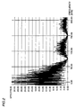
- Spectra according to the above coding methods are shown in Figs. 2 to 5. As can be clearly seen from these graphs, the zero level of each spectrum does not lie within the main lobe band according to the conventional coding methods, and the spectrum is present in the entire main lobe frequency band.
- Japanese Patent Laying-Open No. 7-107125 discloses a method of communicating by repeating the same symbol at least twice.
- the zero level of a spectrum appears within the main lobe band.
- transmission waveforms and spectra when each symbol according to the 4-value PPM method is repeated twice for transmission are shown in Figs. 6 and 7.
- the pulse width is reduced as compared to the bit rate, and the main lobe width of the spectrum increases, which generally makes it difficult to design a receiver.
- the simplest is a method of changing the amplitude, which is called “ASK (Amplitude Shift Keying)" method.
- ASK Amplitude Shift Keying
- ASK Analog to Physical Coding
- the simplest method uses two kinds of amplitudes, in other words a prescribed amplitude and amplitude zero, which is called “OOK (On Off Keying)”. Coding methods by superposing on an output signal according to each of the conventional baseband coding methods a subcarrier for transmission may be considered, which are also ASK coding methods in a broad sense.
- the coding waveforms according to these methods are set forth in Fig. 8.
- PSK Phase Shift Keying
- FSK Frequency Shift Keying
- a spectrum according to a carrier band coding method has a main lobe in a frequency band around a subcarrier frequency.
- a method which uses a plurality of subcarrier frequencies as the FSK method there are a plurality of main lobes in frequency bands around the subcarrier frequencies.
- the width of a sideband of a main lobe according to a carrier band coding method is normally the reciprocal of the minimum "subcarrier non-changing time" used in the coding method.
- a spectrum according to an ASK coding method in which a subcarrier is superposed on an output signal according to a baseband coding method is produced by shifting a spectrum according to the original baseband coding method to a frequency band around the subcarrier.
- the spectrum according to the baseband coding method does not entirely shift to the high frequency band, and a certain amount of the spectrum according to the baseband coding method remains as unnecessary radiation in the low frequency band.
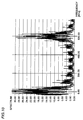
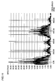
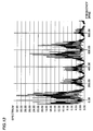
- Spectra according to ASK coding methods produced by superposing subcarriers on the output signals accordingly to the baseband coding methods are set forth in Figs. 10 to 13.
- remote controlls for TV sets usually employ an ASK communication method at a bit rate of about 1 Kbps, using a subcarrier at around 40 kHz, the spectrum of which has a main lobe of about 2 kHz on one side around the vicinity of 40 kHz.
- a baseband coding method or an ASK communication method is employed, a signal spectrum appears in the entire low frequency band up to about 0 Hz - 75 kHz area, which interferes with the optical communication of the remote controll. More specifically, according to a conventional baseband coding method or an ASK coding method, interference between communication at 75 Kbps and remote communication at 40 kHz may be hardly avoided.
- the pulse width is narrowed relative to the bit rate, and the main lobe expands, which makes it difficult to design a receiver.
- Another object of the invention is to provide a baseband transmitter capable of coding transmission data for optical communication, without causing another optical communication device to erroneously operate.
- Yet another object of the invention is to provide a baseband receiver capable of decoding received coded transmission data, without causing another optical communication device to erroneously operate in optical communication.
- a still further object of the invention is to provide an ASK transmitter capable of coding transmission data without causing another optical communication device to erroneously operate in optical communication.
- An additional object of the present invention is to provide an ASK receiver capable of decoding received coded transmission data without causing another optical communication device to erroneously operate in optical communication.
- a method of coding a signal for digital optical communication uses a symbol formed of N slots [S 1 , S 2 , S 3 , ..., S N ], wherein Si is one of 0 and 1 if 1 ⁇ i ⁇ N.
- the method includes the steps of determining a plurality of symbols which satisfy the following expression, wherein k is an arbitrary positive integer, p 1 , q 1 , p 2 , q 2 , ..., p k , q k are integers which satisfy 1 ⁇ p 1 ⁇ q 1 , 1 ⁇ p 2 ⁇ q 2 , ..., 1 ⁇ p k ⁇ q k , p 1 /q 1 ⁇ p 2 /q 2 ⁇ ... ⁇ p k /q k : and coding transmission data based on said determined plurality of symbols.
- a spectrum may have a zero level at a particular frequency, so that another optical communication device may perform optical communication at that particular frequency without erroneous operation.
- a baseband transmitter uses a symbol formed of N slots [S 1 , S 2 , S 3 , ..., S N ], wherein S i is one of 0 and 1 if i is an integer and 1 ⁇ i ⁇ N, the transmitter includes a coding portion for coding transmission data based on a plurality of symbols which satisfy Expression (1) and outputting the coded data as a symbol pattern, if k is an arbitrary positive integer, and p 1 , q 1 , p 2 , q 2 , ..., p k and q k are integers which satisfy 1 ⁇ p 1 ⁇ q 1 , 1 ⁇ p 2 ⁇ q 2 , ..., 1 ⁇ p k ⁇ q k , p 1 /q 1 ⁇ p 2 /q 2 ⁇ p k /q k : and an E/O conversion portion for converting the symbol pattern output by the coding portion into an optical signal.
- the transmission data is coded based on the plurality of symbols which satisfy Expression (1), in the baseband transmitter, a spectrum has a zero level at a particular frequency, and therefore another optical communication device can perform optical communication at that particular frequency without erroneous operation.
- a baseband receiver uses a symbol formed of N slots [S 1 , S 2 , S 3 , ..., S n ], wherein S i is one of 0 and 1 if i is an integer and 1 ⁇ i ⁇ N.
- the baseband receiver includes an O/E conversion portion for converting a received optical signal pattern into a symbol pattern; and a decoding portion for decoding the symbol pattern based on a plurality of symbols which satisfy Expression (1), thereby generating received data, wherein k is an arbitrary positive integer, and p 1 , q 1 , p 2 , q 2 , ..., p k , q k are integers wich satisfy 1 ⁇ p 1 ⁇ q 1 , 1 ⁇ p 2 ⁇ q 2 , ..., 1 ⁇ p k ⁇ q k , and p 1 /q 1 ⁇ p 2 /q 2 ⁇ ... ⁇ p k /q k .
- the baseband receiver can decode received coded data so that the spectrum has a zero level at a particular frequency, another optical communication device can perform optical communication at that particular frequency without erroneous operation.
- an ASK transmitter uses a symbol formed of N slots [S 1 , S 2 , S 3 , ..., S N ], wherein S i is one of 0 and 1 if i is an integer and 1 ⁇ i ⁇ N.
- the transmitter includes a coding portion for coding transmission data based on a plurality of symbols which satisfy Expression (1) and outputting the coded data as a symbol pattern, wherein k is an arbitrary positive integer, and p 1 , q 1 , p 2 , q 2 , ..., p k and q k are integers which satisfy 1 ⁇ p 1 ⁇ q 1 , 1 ⁇ p 2 ⁇ q 2 , ..., 1 ⁇ p k ⁇ q k , and p 1 /q 1 ⁇ p 2 /q 2 ⁇ p k /q k ; a modulation portion for superposing a subcarrier on the symbol pattern output from the coding portion and generating a transmission electrical signal pattern; and an E/O conversion portion for converting the electrical signal pattern generated by the modulation portion into an optical signal.
- the ASK transmitter can have a zero level in a spectrum at a particular frequency, and therefore another optical communication device may perform optical communication at that particular frequency without erroneous operation.
- an ASK receiver uses a symbol formed of N slots [S 1 , S 2 , S 3 , ..., S N ], wherein S i is one of 0 and 1 if i is an integer and 1 ⁇ i ⁇ N.
- the ASK receiver includes an O/E conversion portion for converting a received optical signal pattern into an electrical signal pattern, a detection portion for detecting the electrical signal pattern and generating a symbol pattern, and a decoding portion for decoding the symbol pattern based on a plurality of symbols which satisfy Expression (1) and generating received data, wherein k is an arbitrary positive integer, and p 1 , q 1 , p 2 , q 2 , ..., p k and q k are integers which satisfy 1 ⁇ p 1 ⁇ q 1 , 1 ⁇ p 2 ⁇ q 2 , ..., 1 ⁇ p k ⁇ q k , and p 1 /q 1 ⁇ p 2 /q 2 ⁇ ... ⁇ p k /q k .
- the ASK receiver can decode transmission data coded such that a spectrum has a zero level at a particular frequency, and therefore another optical communication device may perform optical communication at that particular frequency without erroneous operation.
- a particular frequency in the main lobe is defined as follows: wherein k is an arbitrary positive integer, and p 1 , q 1 , p 2 , q 2 , ..., p k and q k are integers which satisfy 1 ⁇ p 1 ⁇ q 1 , 1 ⁇ p 2 ⁇ q 2 , ... 1 ⁇ p k ⁇ q k , and p 1 /q 1 ⁇ q 2 /q 2 ... ⁇ p k /q k .
- Expression (2) has a zero level
- a group of symbols which satisfy Expression (1) are used.
- Expression (1) for Expression (4) nullifies the entire Expression (4). Therefore, it is appreciated that the spectrum of a signal formed of a group of symbol patterns selected to satisfy Expression (1) does not include a component at that particular frequency given by Expression (2).
- bit rate may be set at the level defined by Expression (7) or higher.
- the particular frequency given by Expression (2) at which the spectrum attains a zero level may be set to a value at most twice that of the bit rate frequency. More specifically, a zero level for the signal spectrum may be set at an arbitrary particular frequency equal to or lower than twice the bit rate frequency.
- the bit rate may be set at least at a level defined by the following Expression (9).
- p k N q k 1 NT 0 p k q k 1 T 0
- the particular frequency given by Expression (2) at which the spectrum attains a zero level may be set at a value equal to or lower than the bit rate frequency. More specifically, a zero level may be provided in a signal spectrum at an arbitrary particular frequency equal to or lower than the bit rate frequency.
- a baseband optical transmitter includes a coding portion 200 and an E/O conversion portion 202.
- Coding portion 200 converts 1-bit or multi-bit transmission data 100 into a symbol pattern 101.
- E/O conversion portion 202 drives a light emitting element based on symbol pattern 101, and converts the pattern into a transmission optical signal pattern 103 for transmission.
- a baseband optical receiver includes an O/E conversion portion 203, a clock reproducing portion 205 and a decoding portion 206.
- O/E conversion portion 203 converts a received optical signal pattern 104 into an electrical signal by a light receiving element, then removes noise, amplifies the signal and generates a symbol pattern 106, an electrical signal.
- Clock reproducing portion 205 extracts a clock component included in symbol pattern 106, and reproduces a reproduction clock 107.
- Decoding portion 206 reproduces received data 108 from symbol pattern 106 and reproduction clock 107. Note that although in the above description, the
- transmitter and receiver are separately described, a single transmitter/receiver may be employed.
- the symbol is derived for the purpose of producing a baseband coding method at 75 Kbps, which is unlikely to interfere with a remote control device using a subcarrier at 36, 38 or 40 kHz and by which the signal spectrum attains a zero level at a single particular frequency.
- Coding portion 200 includes conversion table 210 shown in Fig. 16 and a shift register which is not shown.
- Conversion table 210 generates a parallel symbol pattern 110 based on the 4 bit (16 kinds of) transmission data. More specifically, the pattern may be simply formed using a ROM (Read Only Memory) or a logic circuit as follows.
- ROM Read Only Memory
- the shift register sequentially converts parallel symbol pattern 110 into a serial symbol pattern 101.
- E/O conversion portion 202 generates and outputs a transmission optical signal pattern 103 the same as symbol pattern 101.
- a received optical signal pattern 104 is input to O/E conversion portion 203 on the baseband optical receiver side.
- O/E conversion portion 203 converts received optical signal pattern 104 into an electrical signal and outputs the signal as a symbol pattern 106.
- Clock reproducing portion 205 is formed of a PLL (Phase Locked Loop) circuit.
- Decoding portion 206 reproduces received data 108 from reproduction clock 107 reproduced by clock reproduction portion 205 and symbol pattern 106.
- Decoding portion 206 includes a shift register and a conversion table 222 shown in Fig. 17.
- the shift register stores a serial symbol pattern for 8 slots available by sampling symbol pattern 106 by reproduction clock 107, and then outputs the pattern as a parallel symbol pattern 112.
- Conversion table 222 generates received data 108 based on 8-bit parallel symbol pattern 112 as shown in Fig. 17. More specifically, the 4 bit (16 kinds of) received data may be reproduced based on for example a simple logic as follows:
- Fig. 20 is a block diagram of an ASK optical transmitter according to this embodiment.
- a coding portion 200 converts 1 bit or multi-bit transmission data 100 into a symbol pattern 101.
- a modulation portion 201 ASK-modulates a subcarrier by symbol pattern 101 and outputs a transmission electrical signal pattern 102.
- An E/O conversion portion 202' drives a light emitting element according to transmission electrical signal pattern 102, and converts the pattern into a transmission optical signal pattern 103' for transmission.
- Fig. 21 is a block diagram of an ASK optical receiver according to this embodiment.
- An O/E conversion portion 203' converts a received optical signal pattern 104' by a light receiving element into an electrical signal, then removes noise, amplifies the signal and generates a received electrical signal pattern 105.
- Detection portion 204 detects the subcarrier of received electrical signal pattern 105 and reproduces symbol pattern 106.
- a clock reproduction portion 205 extracts a clock component included in symbol pattern 106, and reproduces a reproduction clock 107.
- Decoding portion 206 reproduces received data 108 from symbol pattern 106 and reproduction clock 107.
- transmitter and receiver are separately illustrated in the above description, a single transmitter/receiver may be employed.
- the symbol is derived in order to produce an ASK coding method at 75 Kbps, which is unlikely to interfere with a remote control device using a subcarrier at 36, 38 or 40 kHz, and by which the signal spectrum attains a zero level at a single particular frequency.
- Fig. 22 is a block diagram showing details of the ASK optical transmitter shown in Fig. 20. Transmission data 100 segmented for each 4 bits is transmitted to coding portion 200 on the ASK optical transmitter side. Coding portion 200 is formed of a conversion table 210 and a shift register 211.
- Conversion table 210 is the same as that shown in Fig. 16, and therefore the detailed description is not repeated.
- Shift register 211 sequentially converts a parallel symbol pattern 110 into a serial symbol pattern 101.
- Conversion portion 201 includes a crystal oscillator 212 and an AND gate 213. Since a subcarrier pattern 111 is output from crystal oscillator 212, a transmission optical pattern 102 may be obtained by taking an AND of subcarrier pattern 111 and symbol pattern 101.
- E/O conversion portion 202' is formed of an LED driver 214 and an LED 215. A transmission optical signal pattern 103' in the same pattern as a transmission electrical pattern 102 is output from E/O conversion portion 202'.
- Fig. 23 is a block diagram showing details of the ASK optical receiver shown in Fig. 21.
- a received optical signal pattern 104' is input to O/E conversion portion 203' on the ASK optical receiver side.
- O/E conversion portion 203' includes a PinPD 216, an amplifier 217, and a BPF 218, and outputs a received electrical signal pattern 105.
- the signal is detected by a detector 204 to obtain a symbol pattern 106.
- a clock reproduction portion 205 includes a PLL (Phase Locked Loop) circuit 220.
- Decoding portion 206 reproduces received data 108 from reproduction clock 107 reproduced by clock reproduction portion 205 and symbol pattern 106.
- Decoding portion 206 includes a shift register 221 and a conversion table 222.
- Shift register 221 stores a serial symbol pattern for 8 slots available by sampling symbol pattern 106 by clock 107, and then outputs the pattern as a parallel symbol pattern 112.
- Conversion table 222 is the same as that shown in Fig. 17, and therefore the detailed description is not repeated.
- Fig. 24 shows the spectrum of an ASK coding signal produced by superposing a subcarrier at 600 kHz.
- the symbol is derived for the purpose of producing a baseband coding method or an ASK optical coding method at 75 Kbps, which is unlikely to interfere with a remote control device using a subcarrier at 36, 38, 40 or 56.8 kHz, and by which the signal spectrum attains a zero level at two particular frequencies.
- the first half of the symbol [s1, s2, ..., s8] may express the 8 bit data, and the last half of the symbol is a pattern produced by inverting the bits in the first half.
- symbol group may be applied to baseband optical transmitter and receiver, simply by changing the contents of the conversion tables in Figs. 16 and 17, and by changing the number of bits of the shift register.
- Fig. 22 is used as a block diagram of the ASK transmitter.
- Coding portion 200 includes a conversion table 210 and a shift register 211.
- Conversion table 210 generates a parallel symbol pattern 110 based on 8 bit (256 kinds of) transmission data. More specifically, the pattern may he simply formed using a logic circuit as follows.
- Shift register 211 sequentially converts parallel symbol pattern 110 into a serial symbol pattern 101.
- Modulation portion 201 includes a crystal oscillator 212 and an AND gate 213. Since a subcarrier pattern 111 is output from crystal oscillator 212, a transmission optical signal pattern 102 may be obtained by taking an AND of the subcarrier pattern and symbol pattern 101.
- An E/O conversion portion 202' includes an LED driver 214 and an LED 215. A transmission optical signal patter 103' in the same pattern as a transmission electrical pattern 102 is output from E/O conversion portion 202'.
- Fig. 23 is used as a block diagram of the ASK optical receiver.
- a received optical signal pattern 104' is input to an O/E conversion portion 203' on the ASK optical receiver side.
- O/E conversion portion 203' includes a PiNPD 216, an amplifier 217 and a BPF 218, and outputs a received electrical signal pattern 105.
- a detector 204 detects the signal to produce a symbol pattern 106.
- a clock reproduction portion 205 is formed of a PLL (Phase Locked Loop) circuit 220.
- a decoding portion 206 reproduces received data 108 from a reproduction clock 107 reproduced by clock reproduction portion 205 and symbol pattern 106.
- Decoding portion 206 includes a shift register 221 and a conversion table 222.
- Shift register 221 stores a serial symbol pattern for 16 slots available by sampling symbol pattern 106 by reproduction clock 107, and then outputs a parallel symbol pattern 112.
- the conversion table generates 8-bit received data 108 based on parallel symbol pattern 112. More specifically, 8 bit (256 kinds of) received data may be reproduced based on simple logics for example as follows:
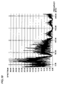
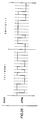
- FIG. 25 A signal waveform and the shape of a signal spectrum in communication by randomly selecting 256 symbol are shown in Figs. 25 and 26, respectively. As shown in Fig. 26, it is confirmed that the bit rate of 75 Kbps is implemented, while a gap may be produced in the spectrum at 37.5 kHz and 56.25 kHz.
- each embodiment may be implemented by changing the contents of conversion tables and the number of bits of the shift register in the baseband optical transmitter and receiver shown in Fig. 14 and 15, or the ASK optical transmitter and receiver as shown in Fig. 20 and 21.
- information of at least 2 bits may be expressed by a single symbol group.
- information of at least 2 bits may be expressed by a single symbol group.
- information of at least 3 bits may be expressed by a single symbol group.
- information of at least 2 bits may be expressed by a single symbol group.
- information of at least 2 bits may be expressed by a single symbol group.
- information of at least 4 bits may be expressed by a single symbol group.
- information of at least 3 bits may be expressed by a single symbol group.
- information of at least 3 bits may be expressed by a single symbol group.
- information of at least 3 bits may be expressed by a single symbol group.
- information of at least 6 bits may be expressed by a single symbol group.
- information of at least 4 bits may be expressed by a single symbol group.
- information of at least 3 bits may be expressed by a single symbol group.
- information of at least 4 bits may be expressed by a single symbol group.
- information of at least 4 bits may be expressed by a single symbol group.
- information of at least 7 bits may be expressed by a single symbol group.
- information of at least 6 bits may be expressed by a single symbol group.
- information of at least 6 bits may be expressed by a single symbol group.
- information of at least 5 bits may be expressed by a single symbol group.
- information of at least 6 bits may be expressed by a single symbol group.
- information of at least 3 bits may be expressed by a single symbol group.
- information of at least 5 bits may be expressed by a single symbol group.
- information of at least 3 bits may be expressed by a single symbol group.
- information of at least 5 bits may be expressed by a single symbol group.
- information of at least 9 bits may be expressed by a single symbol group.
- information of at least 8 bits may be expressed by a single symbol group.
- information of at least 8 bits may be expressed by a single symbol group.
- information of at least 6 bits may be expressed by a single symbol group.
- information of at least 8 bits may be expressed by a single symbol group.
- information of at least 5 bits may be expressed by a single symbol group.
- information of at least 6 bits may be expressed by a single symbol group.
- information of at least 4 bits may be expressed by a single symbol group.
- information of at least 6 bits may be expressed by a single symbol group.
- information of at least 6 bits may be expressed by a single symbol group.
- information of at least 4 bits may be expressed by a single symbol group.
- information of at least 4 bits may be expressed by a single symbol group.
- information of at least 5 bits may be expressed by a single symbol group.
- information of at least 4 bits may be expressed by a single symbol group.
- information of at least 7 bits may be expressed by a single symbol group.
- information of at least 6 bits may be expressed by a single symbol group.
- information of at least 4 bits may be expressed by a single symbol group.
- information of at least 5 bits may be expressed by a single symbol group.
- information of at least 8 bits may be expressed by a single symbol group.
- information of at least 7 bits may be expressed by a single symbol group.
- information of at least 6 bits may be expressed by a single symbol group.
- information of at least 4 bits may be expressed by a single symbol group.
- information of at least 6 bits may be expressed by a single symbol group.
- information of at least 9 bits may be expressed by a single symbol group.
- information of at least 8 bits may be expressed by a single symbol group.
- information of at least 7 bits may be expressed by a single symbol group.
- information of at least 5 bits may be expressed by a single symbol group.
- information of at least 7 bits may be expressed by a single symbol group.
- information of at least 10 bits may be expressed by a single symbol group.
- information of at least 9 bits may be expressed by a single symbol group.
- information of at least 8 bits may be expressed by a single symbol group.
- information of at least 6 bits may be expressed by a single symbol group.
- information of at least 8 bits may -be expressed by a single symbol group.
- information of at least 4 bits may be expressed by a single symbol group.
- information of at least 4 bits may be expressed by a single symbol group.
- the number of slots is preferably from 3 to 16 in practice.
- a single or a plurality of zero levels may be provided in a signal spectrum at a particular frequency(s) within the main lobe frequency band of the signal spectrum, and therefore interference between a plurality of different infrared communication systems including an existing system (such as remote control device) may be alleviated.
Landscapes
- Physics & Mathematics (AREA)
- Spectroscopy & Molecular Physics (AREA)
- Engineering & Computer Science (AREA)
- Computer Networks & Wireless Communication (AREA)
- Signal Processing (AREA)
- Optical Communication System (AREA)
- Dc Digital Transmission (AREA)
Applications Claiming Priority (6)
| Application Number | Priority Date | Filing Date | Title |
|---|---|---|---|
| JP155188/97 | 1997-06-12 | ||
| JP15518897 | 1997-06-12 | ||
| JP15518897 | 1997-06-12 | ||
| JP294250/97 | 1997-10-27 | ||
| JP29425097 | 1997-10-27 | ||
| JP29425097 | 1997-10-27 |
Publications (2)
| Publication Number | Publication Date |
|---|---|
| EP0884865A2 true EP0884865A2 (de) | 1998-12-16 |
| EP0884865A3 EP0884865A3 (de) | 2001-05-30 |
Family
ID=26483257
Family Applications (1)
| Application Number | Title | Priority Date | Filing Date |
|---|---|---|---|
| EP98110454A Withdrawn EP0884865A3 (de) | 1997-06-12 | 1998-06-08 | Verfahren zur Signalkodierung für digitale optische Übertragung |
Country Status (2)
| Country | Link |
|---|---|
| US (2) | US6215826B1 (de) |
| EP (1) | EP0884865A3 (de) |
Cited By (2)
| Publication number | Priority date | Publication date | Assignee | Title |
|---|---|---|---|---|
| WO2002061977A3 (en) * | 2001-02-01 | 2003-02-06 | Ibm | Repetition coding for optical networks of computing devices |
| US6985468B2 (en) | 2000-02-03 | 2006-01-10 | Matsushita Electric Industrial Co., Ltd. | Memory circuit and coherent detection circuit |
Families Citing this family (4)
| Publication number | Priority date | Publication date | Assignee | Title |
|---|---|---|---|---|
| US6977966B1 (en) * | 2000-11-28 | 2005-12-20 | Tellabs Bedford, Inc. | Bidirectional optical communications having quick data recovery without first establishing timing and phase lock |
| EP1597089A2 (de) * | 2003-02-14 | 2005-11-23 | Avery Dennison Corporation | Mehrlagiges trockenfarbenzierlaminat mit sperre zur verhinderung von verfärben |
| EP3704838B1 (de) * | 2017-11-03 | 2023-05-17 | Telefonaktiebolaget LM Ericsson (PUBL) | Sender, netzwerkknoten, verfahren und computerprogramm zur übertragung von binären informationen |
| EP3704839A1 (de) * | 2017-11-03 | 2020-09-09 | Telefonaktiebolaget LM Ericsson (PUBL) | Empfänger, kommunikationsvorrichtung, verfahren und computerprogramm zur empfangen von binären informationen |
Family Cites Families (5)
| Publication number | Priority date | Publication date | Assignee | Title |
|---|---|---|---|---|
| US5768269A (en) * | 1995-08-25 | 1998-06-16 | Terayon Corporation | Apparatus and method for establishing frame synchronization in distributed digital data communication systems |
| US6204889B1 (en) * | 1995-12-15 | 2001-03-20 | Canon Kabushiki Kaisha | Image information processing apparatus |
| US5936578A (en) * | 1995-12-29 | 1999-08-10 | Lucent Technologies | Multipoint-to-point wireless system using directional antennas |
| US6122010A (en) * | 1996-12-16 | 2000-09-19 | Vidicast Ltd. | Television signal data transmission system |
| US6137842A (en) * | 1997-11-28 | 2000-10-24 | The United States Of America As Represented By The Secretary Of The Navy | System and method for determining the time difference of arrival of a frequency shift keyed signal at two separate receivers |
-
1998
- 1998-06-08 EP EP98110454A patent/EP0884865A3/de not_active Withdrawn
- 1998-06-12 US US09/096,989 patent/US6215826B1/en not_active Expired - Fee Related
-
2001
- 2001-02-14 US US09/783,525 patent/US6456667B2/en not_active Expired - Fee Related
Non-Patent Citations (1)
| Title |
|---|
| J.R. BARRY: "wireless infrared communications" 1994 , ACADEMIC PUBLISHERS , KLUWER XP002163613 * page 109, paragraph INTRODUCTION * * page 122, line 6 - page 123, line 32 * * page 127, paragraph * * |
Cited By (4)
| Publication number | Priority date | Publication date | Assignee | Title |
|---|---|---|---|---|
| US6985468B2 (en) | 2000-02-03 | 2006-01-10 | Matsushita Electric Industrial Co., Ltd. | Memory circuit and coherent detection circuit |
| WO2002061977A3 (en) * | 2001-02-01 | 2003-02-06 | Ibm | Repetition coding for optical networks of computing devices |
| US6920289B2 (en) | 2001-02-01 | 2005-07-19 | International Business Machines Corporation | System and method for remote optical digital networking of computing devices |
| US7330662B2 (en) | 2001-02-01 | 2008-02-12 | International Business Machines Corporation | System and method for remote optical digital networking of computing devices |
Also Published As
| Publication number | Publication date |
|---|---|
| US6215826B1 (en) | 2001-04-10 |
| US20010017895A1 (en) | 2001-08-30 |
| EP0884865A3 (de) | 2001-05-30 |
| US6456667B2 (en) | 2002-09-24 |
Similar Documents
| Publication | Publication Date | Title |
|---|---|---|
| US6064697A (en) | Pulse modulating method, pulse modulating equipment and pulse demodulating equipment | |
| KR100446878B1 (ko) | 입력심볼인코딩방법및장치와채널코드워드생성방법및장치 | |
| US20060126751A1 (en) | Technique for disparity bounding coding in a multi-level signaling system | |
| US20080181331A1 (en) | Pulse amplitude modulated system with reduced intersymbol interference | |
| KR20010018672A (ko) | 무직류, 최소대역폭특성을 갖는 선로부호의 설계방법 및 부호화/복호화 장치 | |
| US5103463A (en) | Method and system for encoding and decoding frequency shift keying signals | |
| US6388784B1 (en) | Digital optical transmitter and digital optical receiver making communication by superposing subdata on modulated waveform of main data | |
| US6072829A (en) | Method of higher value step encoding | |
| US6456667B2 (en) | Method of coding signal for digital optical communication having spectrum which attains zero level at prescribed frequency within main lobe band, baseband transmitter or ask transmitter using such method, and baseband receiver or ask receiver decoding signal coded by such method | |
| US4549167A (en) | Method of encoding and decoding binary data | |
| US8044744B2 (en) | Time modulation with cosine function | |
| US6531968B2 (en) | Digital data modulating method and apparatus and modulated data recording medium using the same | |
| US7079577B2 (en) | Wide window decoder circuit for dual phase pulse modulation | |
| US7260151B2 (en) | Dual phase pulse modulation system | |
| JP3769384B2 (ja) | ディジタル光通信用信号の符号化方法、ベースバンド光送信装置、ベースバンド光受信装置、ask光送信装置、及びask光受信装置 | |
| JP2011147087A (ja) | 伝送装置、及び誤り訂正データの付加方法 | |
| US6788743B1 (en) | Modulation of a primary data channel reference clock to form a separate data communication channel | |
| CA2335849A1 (en) | Method for doubling levels of coding | |
| JPH10208404A (ja) | 変調方法、変調装置、復調方法及び復調装置 | |
| KR100356898B1 (ko) | 베이스밴드코드 | |
| KR20050056839A (ko) | 통신 장치 | |
| RU2575005C2 (ru) | Модуляция для передачи кодированного света | |
| EP0534180A2 (de) | Demodulatorschaltung für MSK-Signale | |
| JP2004112100A (ja) | リードチャネル回路及びその復調方法 | |
| JP2005080144A (ja) | シリアル伝送装置のデータ変調・復調方法 |
Legal Events
| Date | Code | Title | Description |
|---|---|---|---|
| PUAI | Public reference made under article 153(3) epc to a published international application that has entered the european phase |
Free format text: ORIGINAL CODE: 0009012 |
|
| AK | Designated contracting states |
Kind code of ref document: A2 Designated state(s): DE FR GB |
|
| AX | Request for extension of the european patent |
Free format text: AL;LT;LV;MK;RO;SI |
|
| PUAL | Search report despatched |
Free format text: ORIGINAL CODE: 0009013 |
|
| RIC1 | Information provided on ipc code assigned before grant |
Free format text: 7H 04B 10/00 A, 7H 04L 25/49 B, 7H 04L 27/06 B, 7H 04L 27/04 B, 7H 04B 10/04 B |
|
| AK | Designated contracting states |
Kind code of ref document: A3 Designated state(s): AT BE CH CY DE DK ES FI FR GB GR IE IT LI LU MC NL PT SE |
|
| AX | Request for extension of the european patent |
Free format text: AL;LT;LV;MK;RO;SI |
|
| 17P | Request for examination filed |
Effective date: 20010802 |
|
| AKX | Designation fees paid |
Free format text: DE FR GB |
|
| 17Q | First examination report despatched |
Effective date: 20040128 |
|
| GRAP | Despatch of communication of intention to grant a patent |
Free format text: ORIGINAL CODE: EPIDOSNIGR1 |
|
| STAA | Information on the status of an ep patent application or granted ep patent |
Free format text: STATUS: THE APPLICATION IS DEEMED TO BE WITHDRAWN |
|
| 18D | Application deemed to be withdrawn |
Effective date: 20050906 |