EP0884934A2 - Substrat und Verfahren zu dessen Herstellung - Google Patents
Substrat und Verfahren zu dessen Herstellung Download PDFInfo
- Publication number
- EP0884934A2 EP0884934A2 EP98304561A EP98304561A EP0884934A2 EP 0884934 A2 EP0884934 A2 EP 0884934A2 EP 98304561 A EP98304561 A EP 98304561A EP 98304561 A EP98304561 A EP 98304561A EP 0884934 A2 EP0884934 A2 EP 0884934A2
- Authority
- EP
- European Patent Office
- Prior art keywords
- layer
- substrate
- principal component
- palladium
- pattern
- Prior art date
- Legal status (The legal status is an assumption and is not a legal conclusion. Google has not performed a legal analysis and makes no representation as to the accuracy of the status listed.)
- Granted
Links
Images




Classifications
-
- H—ELECTRICITY
- H05—ELECTRIC TECHNIQUES NOT OTHERWISE PROVIDED FOR
- H05K—PRINTED CIRCUITS; CASINGS OR CONSTRUCTIONAL DETAILS OF ELECTRIC APPARATUS; MANUFACTURE OF ASSEMBLAGES OF ELECTRICAL COMPONENTS
- H05K3/00—Apparatus or processes for manufacturing printed circuits
- H05K3/10—Apparatus or processes for manufacturing printed circuits in which conductive material is applied to the insulating support in such a manner as to form the desired conductive pattern
- H05K3/18—Apparatus or processes for manufacturing printed circuits in which conductive material is applied to the insulating support in such a manner as to form the desired conductive pattern using precipitation techniques to apply the conductive material
- H05K3/181—Apparatus or processes for manufacturing printed circuits in which conductive material is applied to the insulating support in such a manner as to form the desired conductive pattern using precipitation techniques to apply the conductive material by electroless plating
-
- H—ELECTRICITY
- H05—ELECTRIC TECHNIQUES NOT OTHERWISE PROVIDED FOR
- H05K—PRINTED CIRCUITS; CASINGS OR CONSTRUCTIONAL DETAILS OF ELECTRIC APPARATUS; MANUFACTURE OF ASSEMBLAGES OF ELECTRICAL COMPONENTS
- H05K3/00—Apparatus or processes for manufacturing printed circuits
- H05K3/22—Secondary treatment of printed circuits
- H05K3/24—Reinforcing of the conductive pattern
-
- Y—GENERAL TAGGING OF NEW TECHNOLOGICAL DEVELOPMENTS; GENERAL TAGGING OF CROSS-SECTIONAL TECHNOLOGIES SPANNING OVER SEVERAL SECTIONS OF THE IPC; TECHNICAL SUBJECTS COVERED BY FORMER USPC CROSS-REFERENCE ART COLLECTIONS [XRACs] AND DIGESTS
- Y10—TECHNICAL SUBJECTS COVERED BY FORMER USPC
- Y10S—TECHNICAL SUBJECTS COVERED BY FORMER USPC CROSS-REFERENCE ART COLLECTIONS [XRACs] AND DIGESTS
- Y10S428/00—Stock material or miscellaneous articles
- Y10S428/922—Static electricity metal bleed-off metallic stock
- Y10S428/9335—Product by special process
- Y10S428/934—Electrical process
- Y10S428/935—Electroplating
-
- Y—GENERAL TAGGING OF NEW TECHNOLOGICAL DEVELOPMENTS; GENERAL TAGGING OF CROSS-SECTIONAL TECHNOLOGIES SPANNING OVER SEVERAL SECTIONS OF THE IPC; TECHNICAL SUBJECTS COVERED BY FORMER USPC CROSS-REFERENCE ART COLLECTIONS [XRACs] AND DIGESTS
- Y10—TECHNICAL SUBJECTS COVERED BY FORMER USPC
- Y10S—TECHNICAL SUBJECTS COVERED BY FORMER USPC CROSS-REFERENCE ART COLLECTIONS [XRACs] AND DIGESTS
- Y10S428/00—Stock material or miscellaneous articles
- Y10S428/922—Static electricity metal bleed-off metallic stock
- Y10S428/9335—Product by special process
- Y10S428/936—Chemical deposition, e.g. electroless plating
-
- Y—GENERAL TAGGING OF NEW TECHNOLOGICAL DEVELOPMENTS; GENERAL TAGGING OF CROSS-SECTIONAL TECHNOLOGIES SPANNING OVER SEVERAL SECTIONS OF THE IPC; TECHNICAL SUBJECTS COVERED BY FORMER USPC CROSS-REFERENCE ART COLLECTIONS [XRACs] AND DIGESTS
- Y10—TECHNICAL SUBJECTS COVERED BY FORMER USPC
- Y10T—TECHNICAL SUBJECTS COVERED BY FORMER US CLASSIFICATION
- Y10T428/00—Stock material or miscellaneous articles
- Y10T428/12—All metal or with adjacent metals
- Y10T428/12493—Composite; i.e., plural, adjacent, spatially distinct metal components [e.g., layers, joint, etc.]
- Y10T428/12771—Transition metal-base component
- Y10T428/12861—Group VIII or IB metal-base component
-
- Y—GENERAL TAGGING OF NEW TECHNOLOGICAL DEVELOPMENTS; GENERAL TAGGING OF CROSS-SECTIONAL TECHNOLOGIES SPANNING OVER SEVERAL SECTIONS OF THE IPC; TECHNICAL SUBJECTS COVERED BY FORMER USPC CROSS-REFERENCE ART COLLECTIONS [XRACs] AND DIGESTS
- Y10—TECHNICAL SUBJECTS COVERED BY FORMER USPC
- Y10T—TECHNICAL SUBJECTS COVERED BY FORMER US CLASSIFICATION
- Y10T428/00—Stock material or miscellaneous articles
- Y10T428/12—All metal or with adjacent metals
- Y10T428/12493—Composite; i.e., plural, adjacent, spatially distinct metal components [e.g., layers, joint, etc.]
- Y10T428/12771—Transition metal-base component
- Y10T428/12861—Group VIII or IB metal-base component
- Y10T428/12944—Ni-base component
Definitions
- the present invention relates to a substrate applicable to a circuit board etc., constructed by forming an electroconductive pattern on a glass substrate, and a method for producing the substrate.
- substrates in which the electroconductive pattern is formed on the glass substrate there are the following examples conventionally known as substrates in which the electroconductive pattern is formed on the glass substrate, and production methods thereof.
- an Ag paste is printed on the glass substrate to form a desired electroconductive pattern and it is baked to be fixed.
- a semiconductor layer of ZnO or WO 3 is formed on the glass substrate, thereafter a layer of Pd, Pt, Au, Ag, or the like is deposited thereon by plating, and then an electroconductive layer of Cu or the like is deposited by plating to form the electroconductive pattern (Japanese Laid-open Patent Applications No. 4-17211 and No. 6-61619).
- an undercoat metal layer of nickel is formed on the glass substrate by electroless plating, thereafter an insulating layer is formed in a predetermined pattern thereon, then a metal layer is deposited over exposed portions of the undercoat metal layer by electroplating of copper, the aforementioned insulating layer is then removed, and exposed portions of the undercoat metal layer of nickel is etched away to form a desired electroconductive pattern (Japanese Laid-Open Patent Application No. 8-227656).
- lead glass needs to be added in the paste in order to enhance adhesion to the glass substrate, which increases wire resistance of the electroconductive pattern finally obtained, as compared with bulk Ag.
- a heat treatment near 500°C is necessary for increasing adhesive strength between wires and the substrate, which poses additional problems that the energy cost becomes higher and that warp or strain is more likely to occur in the case wherein the substrate is soda lime glass or the like.
- the semiconductor layer of ZnO or WO 3 is formed on the glass substrate so as to serve as an undercoat layer, a heat treatment at high temperature is necessary in the film-forming process for forming the semiconductor layer of these materials, and thus warp or strain of the glass substrate is likely to occur.
- the nickel plated layer formed on the glass substrate by electroless plating When only the nickel plated layer formed on the glass substrate by electroless plating is used as an undercoat layer, it obviates the need for baking at high temperature necessary in the printing process, but it does not mean that the heat treatment is unnecessary for the substrate. In the case of this process being used, the heat treatment is also necessitated in order to enhance the adhesive strength at the interface between the glass substrate and the nickel plated layer. The reason is that if the plated layer were formed in the thickness enough for wires on the substrate with omitting this heat treatment the risk of exfoliation would increase due to increase in membrane stress.
- the electroless nickel plated layer is baked, for example, at the temperature of about 150°C-300°C, there will arise, however, a problem that an oxide film is formed in the surface of the plated layer to degrade adhesion to a deposit film thereafter. If an attempt is made to remove this oxide film with a chemical, there will often arise a problem that not only the oxide film but also the interface portion between the glass substrate and the nickel plated layer are damaged because of influence of the chemical, so as to degrade the adhesion.
- An object of the present invention is to provide a substrate having a layer structure on a glass substrate with sufficient adhesion between the glass substrate and the electroconductive pattern, without a need for using such a high-temperature process as to cause warp or strain in the glass substrate, and a method for producing the substrate.
- Another object of the present invention is to provide a substrate wherein a layer comprising a principal component of nickel and a layer comprising a principal component of palladium are deposited on a glass substrate and wherein an electroconductive layer is deposited on the palladium layer.
- Still another object of the present invention is to provide a method for producing a substrate, the method comprising a step of forming a layer comprising a principal component of nickel on a glass substrate, a step of forming a layer comprising a principal component of palladium on the nickel layer, and a step of forming an electroconductive layer on the palladium layer.
- the substrate of the present invention can also be formed in such a way that, for enhancing adhesion of the layer comprising the principal component of nickel to the glass substrate, the nickel layer, the layer comprising the principal component of palladium, and the electroconductive layer are deposited after execution of a pretreatment such as a treatment of providing the surface of the glass substrate with catalytic nuclei.
- the production method of the substrate according to the present invention may further comprise a step of a heat treatment for enhancing the adhesive strength of the layer comprising the principal component of nickel to the glass substrate and for enhancing the adhesive strength of the nickel layer to the layer comprising the principal component of palladium.
- the method may further comprise an activation treatment of the surface of the palladium layer in order to enhance the adhesive strength of the palladium layer to the electroconductive layer formed thereon.
- the invention allows use of a reducing agent that does not produce hydrogen as a major side reaction during deposition of metal.
- the substrate and the production method thereof according to the present invention are those as described above.
- the undercoat plated layer is formed by depositing the layer comprising the principal component of nickel as a first layer and the layer comprising the principal component of palladium as a second layer on the glass substrate, whereby formation of the main electroconductive layer by subsequent pattern plating can be performed with sufficient adhesive strength, without using such a high-temperature process as to cause warp or strain in the glass substrate.
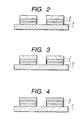
- Figs. 1A to 1E and Figs. 2 to 4 are schematic diagrams to show typical layer structures of the present invention.
- Materials for the glass substrate 1, which can be used in the present invention are alkali-containing glasses generally known as soda lime glass or float glass (for example, trade name: U. F. F Glass available from Nippon Sheet Glass Co., Ltd.), glasses containing little alkali component, generally known as borosilicate glass (for example, trade name: #7059 available from Corning), glasses with an alkali leak preventing layer of SiO 2 or the like on the surface of float glass (for example, trade name: H coat glass available from Nippon Sheet Glass Co., Ltd.), and so on.
- alkali-containing glasses generally known as soda lime glass or float glass
- glasses containing little alkali component generally known as borosilicate glass (for example, trade name: #7059 available from Corning)
- glasses with an alkali leak preventing layer of SiO 2 or the like on the surface of float glass for example
- the layer 2 comprising the principal component of nickel is formed on the glass substrate 1 by electroless plating (Fig. 1A, Fig. 2, Fig. 3, or Fig. 4).
- nickel layer Prior to the formation of the layer comprising the principal component of nickel (hereinafter will also be referred to simply as "nickel layer”), a pretreatment for cleaning the glass substrate is carried out. In order to facilitate deposition of the nickel layer, it is also preferable to provide the surface of the glass substrate with catalytic nuclei, prior to the formation of the nickel layer.
- the treatment for cleaning the glass substrate is normally carried out in several stages and a cleaning agent in this treatment can be a chemical of either a solvent type or a water type.
- a treatment for removing the deteriorated layer of the surface is desirably first carried out by dissolving chromium trioxide in sulfuric acid, diluting it with pure water to prepare a desired aqueous solution (which will be called chromic acid-sulfuric acid), and immersing the substrate in it.
- the glass cleaning agent of the water type can be selected from an aqueous solution of sodium hydroxide and commercially available alkaline surface adjustors.
- the commercially available products are P 3 siliron L or P 3 siliron HS available from Henkel Japan, OPC-380 Condiclean M available from OKUNO CHEMICAL INDUSTRIES CO., LTD., Melcleaner ITO-170 available from MELTEX INC., and so on.
- a method for giving the catalytic nuclei onto the glass substrate 1 is selected from a method for substituting Sn adsorbed on the substrate surface for Pd to form the catalytic nuclei, a method for making the substrate surface adsorbing a Pd-Sn colloid and thereafter eliminating Sn to form the catalytic nuclei, a method for making the substrate surface adsorbing an Sn-free Pd complex and thereafter reducing it to form the catalytic nuclei of nonvalent metal Pd, a method for similarly making the substrate surface adsorbing an Sn-free Pd colloid and thereafter reducing it to form the catalytic nuclei of nonvalent metal Pd, and so on.
- the glass substrate 1 provided with the catalytic nuclei as described above is immersed in the electroless nickel plating solution to form the nickel plated layer 2 (undercoat metal layer).
- the layer comprising the principal component of nickel is a film containing nickel as a principal component, formed by electroless plating.
- the layer comprising the principal component of nickel as described are a nickel plated film, a nickel-phosphorus plated film (hereinafter will also be referred to as " Ni-P plated film"), a film containing nickel and boron, and so on. In either case the point is that the layer contains nickel as a principal component.
- the electroless nickel plating solution used in the present invention had better not have a too large deposition rate, because the film form needs to be as dense as possible and include less defect, from the necessity for direct deposition on the glass substrate.
- an effective way for enhancing adhesion at the interface between the glass substrate and the plated layer is to control the deposition rate of nickel plating in the range of 0.01 ( ⁇ m/min) to 0.15 ( ⁇ m/min), and it is necessary to match the pretreatment system including the surface adjustment and provision of catalytic nuclei with the component design of the electroless nickel plating solution so as to keep the deposition rate in the mentioned range.
- the deposition rate is off the range of 0.01 ( ⁇ m/min) to 0.15 ( ⁇ m/min), for example, when the deposition rate is smaller than 0.01 ( ⁇ m/min), the plated film becomes discontinuous in an island pattern; if the deposition rate is greater than 0.15 ( ⁇ m/min), uniformity of the plated film is degraded. Therefore, either case is not preferred.
- the layer 3 comprising the principal component of palladium is formed on the nickel plated layer 2 (Fig. 1A, Fig. 2, Fig. 3, or Fig. 4).
- the layer comprising the principal component of palladium is a film containing palladium as a principal component, formed by electroless plating.
- Specific examples of the layer containing palladium as a principal component as described are a palladium plated film, a palladium-phosphorus plated film, and so on, and in either case the point is that the layer contains palladium as a principal component.
- the nickel plated layer 2 formed in the present invention functions as an undercoat metal layer for the electroconductive layer formed on this layer.
- the invention also allows us to employ an electroless palladium plating solution containing a reducing agent that does not produce hydrogen as a major side reaction during deposition of palladium.
- the reducing agent used for the electroless palladium plating can be one not producing hydrogen as a major side reaction during deposition of metal and the following examples are generally known as reducing agents used for electroless plating.
- the examples include sodium hypophosphite, sodium borohydride, formaldehyde, dimethylamine borane, trimethylamine borane, methylmorpholino borane, diisopropylamine borane, L-sodium ascorbate, sodium phosphite, tartaric acid, glucose, glycerine, sodium N, N-diethylglycine, sodium formate, sodium citrate, titanium trichloride, hydrazine, thiourea, methylthiourea, N-methylthiourea, N-ethylthiourea, hydroquinone, bivalent cobalt compounds, etc., and many other reducing agents can also be used.
- hydrogen is generated when the reducing agent is selected from dimethylamine borane, sodium borohydride, formaldehyde, sodium hypophosphite, etc., whereas hydrogen is not generated when the reducing agent is selected from hydrazine, thiourea, methylthiourea, N-methylthiourea, N-ethylthiourea, hydroquinone, sodium formate, citric acid, and so on.
- the palladium plated layer can be deposited with avoiding the risk of exfoliation of film due to hydrogen absorption, on a nickel-phosphorus plated thin film on the glass member, where the adhesive strength of the interface is not enhanced sufficiently by the heat treatment.
- a treatment for immersing the substrate in a solution obtained by eliminating the metal component from the electroless palladium plating solution can also be carried out prior to the immersion into the electroless palladium plating solution. This treatment further enhances uniformity of film thickness of the palladium plated layer 3.
- the electroless plating solution used in the present invention is desirably one forming a deposit film with smaller stress.
- the total film thickness will have the following appropriate range.
- the present invention requires the following conditions; the total thickness of the two plated layers, A + B, is 0.05 ⁇ (A + B) ⁇ 1.5 and preferably 0.06 ⁇ (A + B) ⁇ 1.0; the film thickness A of the plated layer 2 is 0.04 ⁇ A and preferably 0.05 ⁇ A; the film thickness B of the plated layer 3 is 0.02 ⁇ B and preferably 0.03 ⁇ B.
- Ni plating solution used in the present invention it is desirable to avoid too large deposition rates of the Ni plating solution used in the present invention, because the Ni plated layer needs to have the form of film as dense as possible and with less defect, from the need for directly depositing the film on the glass substrate.
- Fig. 6 is a graph to show the correlation between the film thickness and plating time, as an example where the pretreatment system is matched with Ni-P plating so as to keep the deposition rate in the above range.
- the plated layer 3 deposited on the plated layer 2 at this time is desirably selected from an electroless Pd plated layer not containing P if importance is placed on heat resistance of the electroconductive pattern, and an electroless Pd-P plated layer if importance is placed on adhesion upon pattern plating, rather than heat resistance.
- the glass substrate is washed well with ion-exchanged water (and further, water adhering to the substrate may be removed by air blow).
- a heat treatment (annealing) of the glass substrate may be carried out, for example, in the ambience of 150°C to 250°C for 30 or more minutes.
- the purpose of this heat treatment is to discharge hydrogen, which is a by-product, for example, of Ni-P deposition reaction and absorbed in the plated layer 2 (undercoat metal layer), so as to enhance adhesive strength between the glass substrate 1 and the plated layer 2, thereby preventing exfoliation of film from occurring during the subsequent photolithographyetching processes.
- the photosensitive photoresist used herein can be any photoresist as long as it has resistance against an etchant comprised of mixed acid, used in the next step.
- Commercially available products to satisfy these conditions are OFPR#700, OMR#83, and Ohdil ⁇ 340 available from TOKYO OHKA KOGYO CO., LTD.
- Fig. 1B is a schematic diagram to show this state wherein the protective resist 4 is formed in the conductive pattern.
- the glass substrate is washed with ion-exchanged water and then is immersed in a chemical for removing the resist 4, thereby removing the now unnecessary protective resist.
- the chemical for removal of the resist 4 used herein can be a commercially available, dedicated remover to each used resist, for example, NMD-3 available from TOKYO OHKA KOGYO CO., LTD, and in addition thereto, a preferred remover is one obtained by adding a chelating agent such as gluconic acid to an aqueous solution which is alkaline with addition of sodium hydroxide and heating it at about 70°C.
- a chelating agent such as gluconic acid
- the mixture ratio and concentration of the aforementioned mixed acid may be adjusted properly.
- the substrate may be exposed to excimer light by use of a dielectric barrier discharge excimer lamp available from USHIO INC., prior to the etching with the mixed acid, thereby enhancing the water wettability of the palladium plated layer 3 exposed.
- Fig. 1C is a schematic diagram of the pattern formed as described above.
- a step of carrying out a heat treatment of the substrate shown in Fig. 1C may be added before formation of the electroconductive layer on the substrate with the plated layers formed in the pattern.
- This heat treatment can be carried out, for example, in the ambience of 100°C to 350°C, preferably in the ambience of 250°C to 350°C, for example, for 30 to 60 minutes.
- the purpose of this heat treatment is to oxidize cross sections of the Ni plated pattern exposed by etching, so as to minimize side etching occurring between the glass substrate 1 and the Ni plated layer 2 with chemicals after the pattern plating.
- the reason why the maximum of the heat treating temperature is 350°C is to avoid the treatment at higher ambient temperature from causing surface oxidation of the Pd plated layer 3, thereby enhancing adhesion of the conductive layer formed on the Pd plated layer 3.
- the reason why the preferred minimum of the heat treatment temperature is 250°C is that the effect of oxidation of the cross sections of the Ni plated pattern is weakened at temperatures lower than 250°C.
- the electroconductive layer 5 can be either an electroplated layer or an electroless-plated layer.
- Figs. 1D and 1E are schematic diagrams where silver (Ag) electroplating is employed.
- the electroplating is not limited to only silver, but the other metals including Au, Pt, Cu, Ni, and Pd can also be arbitrarily plated in the pattern, according to the purpose of use.
- Fig. 2 to Fig. 4 illustrate schematic diagrams in each of which a metal except for Ag is plated in the pattern.
- Fig. 2 is a schematic diagram where an Au plated layer 6 is deposited on the patterned plated layers (the undercoat metal layers) 2, 3 by displacement gold plating.
- Fig. 1D and 1E are schematic diagrams where silver (Ag) electroplating is employed.
- the electroplating is not limited to only silver, but the other metals including Au, Pt, Cu, Ni, and Pd can also be arbitrarily plated in the pattern, according to the purpose of use.
- Fig. 2 to Fig. 4 illustrate schematic diagrams in each of which a metal except for Ag is plated
- FIG. 3 is a schematic diagram where a Pt plated layer 7 is deposited on the patterned plated layers (undercoat metal layers) 2, 3 by electroless plating
- Fig. 4 is a schematic diagram where a Cu plated layer 8 is deposited on the patterned plated layers (undercoat metal layers) 2, 3 by electroplating.
- the electroconductive pattern on the glass substrate 1 showed no film exfoliation even in formation of fine lines with the pattern width of 50 ⁇ m and also passed adhesion-peeling tests by adhesive tape.
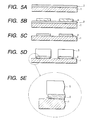
- the pattern-plated layer is formed by Ag electroplating above the glass substrate with only an electroless Ni plated layer as an undercoat metal layer, without employing the layer structure shown in the present invention, the situations are shown in Figs. 5A to 5E. This will be described below in order.
- Fig. 5A is a schematic diagram where a Ni-P plated layer (undercoat metal layer) 2 is formed on the substrate 1 of soda lime glass by electroless plating.
- Fig. 5B is a schematic diagram where the above substrate is baked at the ambient temperature of 170°C for two hours and thereafter the protective resist layer (protective pattern) 4 as described above is formed.
- Fig. 5C is a schematic diagram where the above substrate is etched with the aforementioned mixed acid, thereafter the protective pattern 4 is removed, and then the pattern of Ni-P is formed on the substrate 1.
- Figs. 5D and 5E are schematic diagrams where an Ag plated layer 5 is plated in the pattern on the above substrate by electroplating. Particularly, Fig. 5E shows an enlarged state where after the pattern plating process, the Ni-P plated layer (undercoat metal layer) 2 undergoes side etching, and wraparound of the pattern plated layer 5.
- the electroless plating method When the electroless plating method is employed as a method for forming the electroconductive layer 5, it can be selected from a variety of electroless plating methods.
- desired methods are those using an electroless plating solution containing a reducing agent that does not produce hydrogen as a major side reaction during deposition of metal.
- a desired solution is an electroplating solution with the current efficiency close to 100 %.
- the formation of the electroconductive layer is carried out desirably after the heat treatment for enhancement of adhesive strength between the glass member and the plated layer, different from the occasion of formation of the palladium layer of the second layer as described previously.
- resistance of the interface against hydrogen absorption is improved remarkably, and it is thus adequately possible to perform the deposition using even an electroless plating solution containing a reducing agent that generates hydrogen as a side reaction, or an electroplating solution with not so high current efficiency.
- use of the process with reduced hydrogen absorption is preferred in the case of increase in the thickness of the deposit film or in the case of pattern plating into fine lines.
- Fig. 7, Fig. 8A, and Fig. 8B are examples where the electroconductive layer is deposited using the electroless plating solution containing the reducing agent that produces less hydrogen in side reaction.
- Fig. 7 is a schematic diagram where a platinum plated layer 4 is deposited on a pattern of nickel-phosphorus/palladium formed on the glass substrate, using an electroless platinum plating solution containing the reducing agent of hydrazine.
- Fig. 8A is a schematic diagram where a silver plated layer 5a is deposited similarly, using an electroless silver plating solution containing the reducing agent of hydrazine.
- Fig. 8B is a schematic diagram where a gold plated layer 6a is deposited similarly, using an electroless gold plating solution containing the reducing agent of a thiourea based compound.
- Fig. 8C, Fig. 8D, and Fig. 9A are examples where the electroconductive layer is deposited using the electroplating solution with high current efficiency.
- Fig. 8C is a schematic diagram where a silver plated layer 5b is deposited on the pattern of nickel-phosphorus/palladium formed on the glass substrate, using a silver electroplating solution.
- Fig. 8D is a schematic diagram where a copper plated layer 7 is deposited similarly, using a copper electroplating solution.
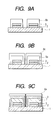
- Fig. 9A is a schematic diagram where a gold plated layer 6b is deposited similarly, using a gold electroplating solution.
- the electroconductive layer can be any other deposit layer including the third layer and subsequent layer of nickel, palladium, or a metal that can be plated in a wet method, than those described above, and Fig. 9B and Fig. 9C are schematic diagrams to show such examples.
- Fig. 9B is a schematic diagram where the surface portion of the silver plated layer 5a of the deposit pattern shown in Fig. 8A is replaced by the replacement gold plating method, thereby forming a gold plated layer 6c.
- Fig. 9C is a schematic diagram where an electroless palladium plated layer 3 is deposited on the copper plated layer 7 of the deposit pattern shown in Fig. 8D and a further electroless gold plated layer 6a is deposited thereon.
- the adhesion of the electroconductive layer can be further enhanced by carrying out an activation treatment to activate the surface of the palladium layer after patterning after formation of the nickel layer and palladium layer on the glass substrate and before formation of the electroconductive layer 5.
- the activation treatment is, for example, one or more of the following treatments [a], [b], [c].
- This treatment is to remove an oxide film formed in the surface of the deposited layer by the heat treatment at 150°C to 250°C, which is desired to be carried out for enhancement of adhesion, and organic substance deposited on the plated layer after removal of the protective resist, thereby further enhancing the reactivity of plating during deposition and adhesion of the interface.
- the metal chelating agent used can be sodium gluconate, hexasodium triethylenetetramine hexaacetic acid, or the like, and the activation treatment is carried out by dissolving either of these and either sodium hydroxide or tetramethylammonium hydroxide in ion-exchanged water, heating it at about 50°C to 80°C, and immersing the substrate therein.
- the activation treatment can be conducted by immersing the substrate in an aqueous solution obtained by diluting hydrochloric acid, sulfuric acid, or the like with ion-exchanged water, or an aqueous solution obtained by further adding a chemical of the iron salt type thereto.
- An example of the commercial product of the activating agent of this mixed type is OPC-91 available from OKUNO CHEMICAL INDUSTRIES CO., LTD.
- the activation treatment can be carried out using the excimer light having a peak of spectral distribution at the wavelength of 172 (nm), as the light of wavelengths in the ultraviolet region for the exposure.
- a device for emitting such light of the wavelengths is, for example, an excimer light radiating device incorporating the dielectric barrier discharge excimer lamp available from USHIO INC.
- Each of the above treatments [a], [b], [c] alone exhibits the sufficient effect as an activation treatment, but they can be employed in combination.
- the treatment of [c] is first carried out, then the treatment of [a] is carried out, followed by sufficient washing with ion-exchanged water, and the treatment of [b] is carried out, whereby the time for each treatment can be decreased and the risk of damage to the substrate and the plated layers can be minimized.
- the metalized glass substrate can be fabricated with excellent chemical resistance, excellent patterning property, and excellent deposition property, with high adhesion, with less film defect, and with suppressing deformation and distortion of the glass substrate even on a smooth glass substrate, and the metalized glass substrate thus obtained can be used, for example, as wires or electrodes for flat panel displays, and also be utilized as plated patterns for solder bumps.
- the glass substrate used herein was a soda lime glass measuring 100 mm ⁇ 100 mm ⁇ thickness 1.1 mm (available from Nippon Sheet Glass Co., Ltd.), and pretreatments of the substrate were carried out according to the following procedures.
- Pretreatment 1 chromium trioxide 100 (g/l) and conc sulfuric acid 200 (g/l) were mixed and ion-exchanged water was added thereto up to the total amount 1 (l), followed by heating to 60°C. The substrate was immersed in the solution of 60°C for an hour and thereafter washed with ion-exchanged water.
- Pretreatment 2 The substrate was immersed under ultrasonic vibration at the bath temperature 70°C in 10 (N) NaOH solution for an hour and thereafter was washed with ion-exchanged water.
- Pretreatment 3 P 3 siliron HS available from Henkel Japan was dissolved in 3 wt% in ion-exchanged water and the substrate was immersed under ultrasonic vibration at the bath temperature 70°C in this solution for an hour. Thereafter, the substrate was washed with ion-exchanged water.
- Pretreatment 4 A chemical containing ammonium fluoride was dissolved in ion-exchanged water and the substrate was immersed under liquid circulation at the bath temperature 25°C in this acid solution for 20 minutes, followed by washing with ion-exchanged water.
- Pretreatment 5 A chemical containing an amino group was dissolved in ion-exchanged water and the substrate was immersed under liquid circulation at the bath temperature 25°C in this weak alkaline solution for 2 minutes, followed by washing with ion-exchanged water.
- Pretreatment 6 PdCl 2 was dissolved in ion-exchanged water to 0.52 (g/l) and pH thereof was adjusted to pH 6.5 with alkali. The substrate was immersed in this solution at the bath temperature 25°C for 2 minutes and then immersed in ion-exchanged water.
- Pretreatment 7 A hypophosphite was dissolved in ion-exchanged water to pH 5.3. The substrate was immersed in the solution at the bath temperature 25°C for one minute and then immersed in ion-exchanged water.
- the glass substrate was put in the electroless Ni-P plating solution having the deposition rate as shown in the graph of Fig. 6 to undergo plating for 6 minutes. After that, the substrate was immersed in ion-exchanged water heated at 50°C to wash away the electroless Ni-P plating solution adhering to the substrate surface. Then the substrate was put in the electroless Pd plating solution heated at 60°C to undergo plating for one minute.
- the electroless Pd plating solution used in the present example was one of a type not causing co-deposition of P and B during deposition of Pd (for example, trade name: PARED available from KOJIMA CHEMICALS).
- the substrate was washed well under running water of ion-exchanged water and then ion-exchanged water adhering to the substrate was removed by air blow. Then the substrate underwent the heat treatment in the ambience of 170°C for two hours to obtain the substrate having the layer structure shown in Fig. 1A.
- the substrate after this heat treatment was slowly cooled down to room temperature and then OFPR-800 available from TOKYO OHKA KOGYO CO., LTD was applied onto the substrate by spin coater. Then the substrate was prebaked in the ambience of 90°C for 30 minutes and underwent exposure with a mask having the pattern of 50 ( ⁇ m). Then the pattern was developed by NMD-3 available from TOKYO OHKA KOGYO CO., LTD, followed by washing under running water of ion-exchanged water. Then the substrate was postbaked in the ambience of 140°C for 30 minutes to obtain the substrate with the protective pattern shown in Fig. 1B.
- This substrate with the protective pattern was immersed at room temperature in the aforementioned mixed acid solution for one minute and then was washed well under running water of ion-exchanged water to obtain the pattern of the undercoat metal layers shown in Fig. 1C.
- the- substrate underwent the heat treatment in the ambience of 300°C for 30 minutes, prior to pattern electroplating of Ag over the pattern of the undercoat metal layers.
- the mean surface roughness of the plated surface of this substrate after the heat treatment and the mean surface roughness of the surface of the glass substrate after peeling of the plated layer were measured using a surface roughness measuring device available from Tencor Inc.
- the electrolytic Ag plating solution used herein was S-900 available from N. E. CHEMCAT CORPORATION the plating was conducted at the bath temperature 60°C and at the current density 0.2 (A/cm 2 ) for 2 minutes, followed by washing with ion-exchanged water. Then the substrate was baked in the ambience of 200°C for an hour.
- the pattern plated substrate fabricated as described above had the layer structure as shown in Fig. 1D. The stripping test by tape was conducted and no line was peeled off thereby.
- the substrate having the layer structure as shown in Fig. 1D was produced under the same conditions as in Example 1 except that the electroless Pd-P plating solution available from OKUNO CHEMICAL INDUSTRIES CO., LTD. replaced the electroless Pd plating solution in Example 1.
- the electroless Pd-P plating conditions employed herein were as follows.
- the substrate obtained in this way had the layer structure as shown in Fig. 1D and no line was peeled off in the stripping test by tape.
- the substrate having the Au plated layer 6 as shown in Fig. 2 was produced under the same conditions as in Example 1 except that the electroless Au plating solution available from Daiwa Kasei replaced the electrolytic Ag plating solution in Example 1.
- the electroless Au plating conditions employed herein were as follows.
- the substrate obtained in this way had the layer structure as shown in Fig. 2 and no line was peeled off in the stripping test by tape.
- the substrate having the Au plated layer 6 as shown in Fig. 2 was produced under the same conditions as in Example 2 except that the electroless Au plating solution available from Daiwa Kasei replaced the electrolytic Ag plating solution in Example 2.
- the electroless Au plating conditions employed herein were as follows.
- the substrate obtained in this way had the layer structure as shown in Fig. 2 and no line was peeled off in the stripping test by tape.
- the substrate having the Pt plated layer 7 as shown in Fig. 3 was produced under the same conditions as in Example 1 except that the electroless Pt plating solution available from N. E. CHEMCAT CORPORATION replaced the electrolytic Ag plating solution in Example 1.
- the electroless Pt plating conditions employed herein were as follows.
- the substrate obtained in this way had the layer structure as shown in Fig. 3 and no line was peeled off in the stripping test by tape.
- the substrate having the Pt plated layer 7 as shown in Fig. 3 was produced under the same conditions as in Example 2 except that the electroless Pt plating solution available from N. E. CHEMCAT CORPORATION replaced the electrolytic Ag plating solution in Example 2.
- the electroless Pt plating conditions employed herein were as follows.
- the substrate obtained in this way had the layer structure as shown in Fig. 3 and no line was peeled off in the stripping test by tape.
- the substrate having the Cu plated layer 8 as shown in Fig. 4 was produced under the same conditions as in Example 1 except that the electrolytic Cu plating solution replaced the electrolytic Ag plating solution in Example 1.
- the composition and conditions of electrolytic Cu plating employed herein were as follows.
- the substrate obtained in this way had the layer structure shown in Fig. 4 and no line was stripped off in the stripping test by tape.
- the substrate having the Cu plated layer 8 as shown in Fig. 4 was produced under the same conditions as in Example 2 except that the electrolytic Cu plating solution replaced the electrolytic Ag plating solution in Example 2.
- the composition and conditions of electrolytic Cu plating employed herein were as follows.
- the substrate obtained in this way had the layer structure shown in Fig. 4 and no line was stripped off in the stripping test by tape.
- Example 2 The same pretreatments as in Example 1 were effected on the substrate of soda lime glass and the metalized substrate as shown in Fig. 5A was produced under the same electroless Ni-P plating conditions. This was baked in the ambience of 170°C for 2 hours. Then the protective layer 4 as shown in Fig. 5B was formed on this Ni-P plated layer under the same process conditions as in Example 1. Then etching was carried out with the mixed acid, thereby forming the Ni-P plated pattern as shown in Fig. 5C.
- the substrate was washed well after the above etching, but the heat treatment was not carried out. Then the substrate underwent the same electrolytic Ag plating as in Example 1, thereby producing the pattern-plated substrate having the layer structure as shown in Fig. 5D. At this time, some parts of the 50 ( ⁇ m) pattern were peeled off under running water of ion-exchanged water after the above electrolytic Ag plating.
- the Ag plated layer was not deposited in a film shape and completely peeled off during washing with ion-exchanged water after the plating.
- the glass substrate used herein was a float glass substrate measuring 100 (mm) x 100 (mm) x thickness 1.1 (mm) (available from Nippon Sheet Glass Co., Ltd.) and the pretreatments were carried out according to the following procedures.
- Chromium trioxide (chromic anhydride) 60 (g/l) and conc sulfuric acid 180 (g/l) were mixed and ion-exchanged water was added up to the total amount 1 (l). This was heated to 70°C and the substrate was immersed therein for an hour, followed by washing with ion-exchanged water.
- the substrate was immersed under ultrasonic vibration in the bath of 10 (N) NaOH solution heated at 70°C for an hour and thereafter was washed under ultrasonic vibration in ion-exchanged water heated at 50°C, followed by washing with ion-exchanged water at room temperature.
- P 3 siliron HS available from Henkel Japan was dissolved in 3 (g/l) in ion-exchanged water and the solution was heated to 70°C. Then the substrate was immersed under ultrasonic vibration in the bath of the solution for an hour and thereafter washed under ultrasonic vibration in ion-exchanged water heated at 50°C, followed by washing with ion-exchanged water at room temperature.
- the chemical containing ammonium fluoride was dissolved in ion-exchanged water to prepare an acid solution and the substrate was immersed in the acid solution controlled at 25 ⁇ 2°C under liquid circulation for 5 minutes, followed by washing with ion-exchanged water at room temperature.
- An aqueous solution was prepared by dissolving the chemical containing the amino group in ion-exchanged water and the substrate was immersed under liquid circulation in the aqueous solution controlled at 25 ⁇ 2°C for 2 minutes, followed by washing with ion-exchanged water at room temperature.
- Palladium chloride (PdCl 2 ) was dissolved in ion-exchanged water to amount 0.5 (g/l) and then pH was adjusted to pH 6.5 with alkali. After that, the bath temperature was controlled to 25 ⁇ 2°C and the substrate was immersed in the bath for 2 minutes and then in ion-exchanged water at room temperature.
- the glass substrate was immersed in the electroless nickel-phosphorus plating solution having the aforementioned deposition rate, heated at 70°C, to undergo plating for 3 minutes, thereby forming the nickel-phosphorus alloy plated layer in the thickness 0.2 ( ⁇ m) over the entire surface of the substrate.
- the electroless nickel-phosphorus plating solution used in the present example was one containing a hypophosphite as a reducing agent.
- the electroless palladium plating solution was one not containing a reducing agent causing co-deposition of P and B during deposition of palladium, i.e., one not containing a reducing agent of a phosphate type and an amine-borane type, and further, not using a reducing agent that generates hydrogen as a side reaction of the deposition of plated layer.
- a reducing agent causing co-deposition of P and B during deposition of palladium
- An example of commercially available electroless palladium plating solution to meet this condition is trade name: PARED available from KOJIMA CHEMICALS.
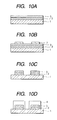
- the substrate was washed well with ion-exchanged water and the ion-exchanged water adhering to the substrate was removed by nitrogen blow. Then the substrate was kept at 170°C in the atmosphere for an hour to obtain the substrate having the layer structure shown in Fig. 10A.
- the substrate after this heat treatment was cooled down to room temperature and thereafter exposed to the excimer light having the peak of spectral distribution at the wavelength of 172 (nm), emitted from the position of 5 (mm) to the substrate by the excimer light radiating device incorporating the dielectric barrier discharge excimer lamp available from USHIO INC., for 30 seconds.
- the trade name OFPR-800 which was a photoresist available from TOKYO OHKA KOGYO CO., LTD, was applied onto this substrate by spin coater, and thereafter the substrate was prebaked in the ambience of 90°C for 30 minutes.
- L/S line-and-space
- the pattern was developed with trade name NMD-3 as a developing agent available from TOKYO OHKA KOGYO CO., LTD, followed by washing under running water of ion-exchanged water.
- the water was removed by nitrogen blow and the substrate was postbaked in the ambience of 140°C for 30 minutes and cooled down to the room temperature. After that, the substrate was again exposed to the aforementioned excimer light for 30 seconds to obtain the substrate having the protective pattern shown in Fig. 10B.
- the aforementioned exposure to the excimer light can be omitted if the pattern width of the protective resist formed is wide enough.
- the substrate with the protective pattern obtained above was immersed at room temperature in the aforementioned mixed acid solution for 45 seconds to etch and remove the exposed plated layers, followed by sufficient washing under running water of ion-exchanged water. Further, the substrate was immersed in a resist remover to remove the protective resist.
- the resist remover used herein was one obtained by dissolving 150 (g) of sodium hydroxide and 10 (g) of sodium gluconate in 1 (l) of ion-exchanged water and heated at 70°C, and the substrate was immersed in this bath for 20 seconds and then washed, thereby obtaining the substrate having the layer structure shown in Fig. 10C.
- the substrate after the above activation treatment was immersed in the electroless silver plating solution to form a silver plated layer 4, thus producing the layered pattern shown in Fig. 10D.
- the electroless silver plating solution used herein was trade name EL-Ag#31 available from N. E. CHEMCAT CORPORATION, and the plating was conducted in pH 10 and at the bath temperature 73°C for an hour to deposit the silver plated layer in the thickness of 1.3 ( ⁇ m).
- the pattern-plated substrate produced in this way underwent the stripping test by tape at the pattern of L/S of 50 ( ⁇ m)/50 ( ⁇ m), and no exfoliation was observed at the interface between the glass substrate and the plated layer, thus demonstrating good adhesion.
- the surface of the glass substrate 1, exposed on the substrate was checked by trade name P-10, which was the surface roughness measuring device available from Tencor Inc., and the mean surface roughness thereof was 0.8 (nm).
- Example 9 On the pattern of L/S of 50 ( ⁇ m)/50 ( ⁇ m), after the electroless silver plating in Example 9, a further silver plated layer was deposited in the thickness 4 ( ⁇ m) by electrolytic silver plating.
- the electrolytic silver plating solution used herein was trade name S-900 available from N. E. CHEMCAT CORPORATION, and the plating conditions were the bath temperature 60°C and the current density 0.2 (A/cm 2 ).
- the pattern-plated substrate produced as described above had the layer pattern as shown in Fig. 10D and this substrate underwent the stripping test by tape at the pattern of L/S of 50 ( ⁇ m)/50 ( ⁇ m). After the stripping test, no exfoliation was observed at the interface between the glass substrate and the plated layer, thus demonstrating good adhesion.
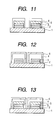
- a gold plated layer 6 for antioxidation was further deposited in the thickness 0.05 ( ⁇ m), thus producing the substrate having the layer structure as shown in Fig. 12.
- the gold plating solution used herein was trade name: Daingold, which was the electroless gold plating solution available from Daiwa Kasei, and plating was carried out at the bath temperature 70°C.
- the pattern-plated substrate produced in this way underwent the stripping test by tape at the pattern of L/S of 50 ( ⁇ m)/50 ( ⁇ m), and no exfoliation was observed at the interface between the glass substrate and the plated layer, thus demonstrating good adhesion.
- Example 9 the pattern of nickel-phosphorus plated layer 2 and palladium plated layer 3 was formed on the glass substrate and activated, and thereafter a copper plated layer 5 was deposited thereon. Then, in the same manner as in Example 9, the silver plated layer 4 was deposited in the thickness 1.0 ( ⁇ m), thus obtaining the substrate having the layer structure as shown in Fig. 11.
- the copper plating solution used herein was trade name: CUST-2000, which was the electroless copper plating solution available from Hitachi Chemical Co., Ltd. (Hitachi Kasei Kogyo), and plating was carried out at the bath temperature 40°C for 2 minutes, thus depositing the copper plated layer 5 in the thickness of 0.6 ( ⁇ m).
- the pattern plated substrate produced in this way underwent the stripping test by tape at the pattern of L/S of 50 ( ⁇ m)/50 ( ⁇ m), and no exfoliation was observed at the interface between the glass substrate and the plated layer, thus demonstrating good adhesion.
- Example 12 On the pattern of L/S of 50 ( ⁇ m)/50 ( ⁇ m), after the electroless silver plating in Example 12, a further silver plated layer 4 was deposited in the thickness 4 ( ⁇ m) by electrolytic silver plating.
- the electrolytic silver plating solution used herein was trade name S-900 available from N. E. CHEMCAT CORPORATION, and the plating conditions were the bath temperature 60°C and the current density 0.2 (A/cm 2 ).
- the pattern-plated substrate produced as described above had the layer pattern as shown in Fig. 11 and this substrate underwent the stripping test by tape at the pattern of L/S of 50 ( ⁇ m)/50 ( ⁇ m). After the stripping test, no exfoliation was observed at the interface between the glass substrate and the plated layer, thus demonstrating good adhesion.
- a gold plated layer 6 for antioxidation was further deposited in the thickness 0.05 ( ⁇ m), thus producing the substrate having the layer structure as shown in Fig. 13.
- the gold plating solution used herein was trade name: Daingold, which was the electroless gold plating solution available from Daiwa Kasei, and plating was carried out at the bath temperature 70°C.
- the pattern-plated substrate produced in this way underwent the stripping test by tape at the pattern of L/S of 50 ( ⁇ m)/50 ( ⁇ m), and no exfoliation was observed at the interface between the glass substrate and the plated layer, thus demonstrating good adhesion.
- the substrates having the layer structures as shown in Fig. 10D to Fig. 13 were produced by the same treatments except that the activation treatment carried out in Examples 9 to 14 was carried out under the following conditions.
- the substrates were prepared by removing the protective resist and carrying out the treatments up to the state shown in Fig. 10C, and then underwent the activation treatment in the following manner.
- the substrates were exposed to the aforementioned excimer light for one minute and then immersed in a treating solution obtained by dissolving 80 (g) of hexasodium triethylenetetramine hexaacetic acid (40 to 45 % aqueous solution) and 200 (g) of sodium hydroxide in ion-exchanged water to amount 1 (l), at 70°C for 5 minutes, followed by washing with ion-exchanged water.
- the substrates were immersed at room temperature in 2 % aqueous solution of trade name OPC-91 available from OKUNO CHEMICAL INDUSTRIES CO., LTD. for 20 seconds, followed by washing with ion-exchanged water.
- the pattern-plated substrates produced in this way underwent the stripping test by tape at the pattern of L/S of 50 ( ⁇ m)/50 ( ⁇ m), and no exfoliation was observed at the interface between the glass substrate and the plated layer, thus demonstrating good adhesion.
- the alkali-containing glass used in Examples 9 to 15 was replaced by trade name: #7059 available from Corning Inc., which was a glass substrate containing little alkali component, generally known borosilicate glass.
- the substrates having the layer structures as shown in Fig. 10D to Fig. 13 were prepared under the same treatment conditions as in Examples 9 to 15, except for the above.
- the pattern-plated substrates produced in this way underwent the stripping test by tape at the pattern of L/S of 50 ( ⁇ m)/50 ( ⁇ m), and no exfoliation was observed at the interface between the glass substrate and the plated layer, thus demonstrating good adhesion. It was also confirmed by electron micrograph at this time that the pattern of L/S of 5 ( ⁇ m)/5 ( ⁇ m) had no disconnection, either.
- the glass substrates used in Examples 9 to 16 were replaced by trade name: H coat glass available from Nippon Sheet Glass Co., Ltd., which was a substrate obtained by forming the SiO 2 layer as an alkali leak preventing layer on the surface of float glass.
- the substrates having the layer structures as shown in Fig. 10D to Fig. 13 were produced under the same treatment conditions as in Examples 9 to 15, except for the above.
- the pattern-plated substrates produced in this way underwent the stripping test by tape at the pattern of L/S of 50 ( ⁇ m)/50 ( ⁇ m), and no exfoliation was observed at the interface between the glass substrate and the plated layer, thus demonstrating good adhesion.
- the alkali glass substrate underwent the pretreatments under the same conditions as in Example 9 and the nickel-phosphorus plated layer 2 was deposited in the thickness 0.3 ⁇ m thereon. After that, the substrate was kept at 170°C in the atmosphere for an hour, and patterning was carried out under the same conditions as in Example 9, followed by removal of the protective resist.
- This comparative example is different from the present invention in that the palladium plated layer is excluded.
- the activation treatment was performed using the aqueous solution containing sodium gluconate and sodium hydroxide, which was the same as in Example 9, but the nickel-phosphorus plated layer 2 was deteriorated thereby.
- the activation treatment was conducted by exposure to the excimer light and immersion in diluted hydrochloric acid for a short time, and the substrate was immersed in the electroless silver plating solution.
- the glass substrate used herein was the float glass substrate measuring 100 (mm) ⁇ 100 (mm) ⁇ thickness 1.1 (mm) (available from Nippon Sheet Glass Co., Ltd.) and the pretreatments were carried out according to the following procedures.
- Chromium trioxide (chromic anhydride) 60 (g/l) and conc sulfuric acid 180 (g/l) were mixed and ion-exchanged water was added up to the total amount 1 (l). This was heated to 70°C and the substrate was immersed therein for an hour, followed by washing with ion-exchanged water.
- the substrate was immersed under ultrasonic vibration in the bath of 10 (N) NaOH solution heated at 70°C for an hour and thereafter was washed under ultrasonic vibration in ion-exchanged water heated at 50°C, followed by washing with ion-exchanged water at room temperature.
- P 3 siliron HS available from Henkel Japan was dissolved in 3 (g/l) in ion-exchanged water and the solution was heated to 70°C. Then the substrate was immersed under ultrasonic vibration in the bath of the solution for an hour and thereafter washed under ultrasonic vibration in ion-exchanged water heated at 50°C, followed by washing with ion-exchanged water at room temperature.
- the chemical containing ammonium fluoride was dissolved in ion-exchanged water to prepare an acid solution and the substrate was immersed in the acid solution controlled at 25 ⁇ 2°C under liquid circulation for 5 minutes, followed by washing with ion-exchanged water at room temperature.
- An aqueous solution was prepared by dissolving the chemical containing the amino group in ion-exchanged water and the substrate was immersed under liquid circulation in the aqueous solution controlled at 25 ⁇ 2°C for 2 minutes, followed by washing with ion-exchanged water at room temperature.
- Palladium chloride (PdCl 2 ) was dissolved in ion-exchanged water to amount 0.5 (g/l) and then pH was adjusted to pH 6.5 with alkali. After that, the bath temperature was controlled to 25 ⁇ 2°C and the substrate was immersed in the bath for 2 minutes and then in ion-exchanged water at room temperature.
- the glass substrate was immersed in the electroless nickel-phosphorus plating solution having the aforementioned deposition rate, heated at 70°C, to undergo plating for 3 minutes, thereby forming the nickel-phosphorus alloy plated layer in the thickness 0.2 ( ⁇ m) over the entire surface of the substrate.
- the electroless nickel-phosphorus plating solution adhering to the substrate surface was washed away in ion-exchanged water heated at 50°C, and then the substrate was immersed in the electroless palladium plating solution heated at 65°C to undergo plating for 45 seconds, thereby depositing the palladium plated layer in the thickness 0.1 ( ⁇ m).
- the electroless nickel-phosphorus plating solution used in the present example was one containing a hypophosphite as a reducing agent.
- the electroless palladium plating solution was one not containing a reducing agent causing co-deposition of P and B during deposition of palladium, i.e., one not containing a reducing agent of the phosphate type and the amine-borane type, and further, not using a reducing agent that generates hydrogen as a side reaction of the deposition of the plated layer.
- An example of the commercially available electroless palladium plating solution to meet this condition is trade name: PARED available from KOJIMA CHEMICALS.
- the substrate was washed well with ion-exchanged water and the ion-exchanged water adhering to the substrate was removed by nitrogen blow. Then the substrate was kept at 170°C in the atmosphere for an hour to obtain the substrate having the layer structure shown in Fig. 10A.
- the substrate after this heat treatment was cooled down to room temperature and thereafter exposed to the excimer light having the peak of spectral distribution at the wavelength of 172 (nm), emitted from the position of 5 (mm) to the substrate by the excimer light radiating device incorporating the dielectric barrier discharge excimer lamp available from USHIO INC., for 30 seconds.
- This is a treatment for enhancing the wettability of the substrate so as to enhance the uniform coating property of the resist and this treatment can be omitted.
- the trade name OFPR-800 which was a photoresist available from TOKYO OHKA KOGYO CO., LTD, was applied onto this substrate by spin coater, and thereafter the substrate was prebaked in the ambience of 90°C for 30 minutes.
- L/S line-and-space
- the pattern was developed with trade name NMD-3 as a developing agent available from TOKYO OHKA KOGYO CO., LTD, followed by washing under running water of ion-exchanged water.
- the water was removed by nitrogen blow and the substrate was postbaked in the ambience of 140°C for 30 minutes and cooled down to the room temperature. After that, the substrate was again exposed to the aforementioned excimer light for 30 seconds to obtain the substrate having the protective pattern shown in Fig. 10B.
- the aforementioned exposure to the excimer light can be omitted if the pattern width of the protective resist formed is wide enough.
- the substrate with the protective pattern obtained above was immersed at room temperature in the aforementioned mixed acid solution for 45 seconds to etch and remove the exposed plated layers, followed by sufficient washing under running water of ion-exchanged water. Further, the substrate was immersed in the resist remover to remove the protective resist.
- the resist remover used herein was one obtained by dissolving 150 (g) of sodium hydroxide and 10 (g) of sodium gluconate in 1 (l) of ion-exchanged water and heated at 70°C, and the substrate was immersed in this bath for 20 seconds and then washed, thereby obtaining the substrate having the layer structure shown in Fig. 10C.
- the substrate after the above activation treatment was immersed in the electroless platinum plating solution to form the platinum plated layer 4, thus producing the layered pattern shown in Fig. 10D.
- the electroless platinum plating solution used herein was trade name EL-Pt available from N. E. CHEMCAT CORPORATION, which was of the type not generating hydrogen as a side reaction during deposition of platinum.
- Plating was carried out in pH 10 and at the bath temperature 70°C for 30 minutes to deposit the platinum plated layer in the thickness of 0.24 ( ⁇ m).
- the pattern-plated substrate produced in this way underwent the stripping test by tape at the pattern of L/S of 50 ( ⁇ m)/50 ( ⁇ m), and no exfoliation was observed at the interface between the glass substrate and the plated layer, thus demonstrating good adhesion.
- the surface of the glass substrate 1, exposed on the substrate was checked by trade name P-10, which was the surface roughness measuring device available from Tencor Inc., and the mean surface roughness thereof was 0.8 (nm).
- the treatments up to the activation treatment were carried out in the same manner as in Example 18 and then the platinum plated layer was deposited by electrolytic platinum plating in the thickness of 0.5 ( ⁇ m) on the pattern of L/S of 50 ( ⁇ m)/50 ( ⁇ m) in the layer structure shown in Fig. 10C.
- the electrolytic platinum plating solution used herein was trade name Pt-745 available from N. E. CHEMCAT CORPORATION, and the plating conditions were pH 12.5, the bath temperature 77°C, and the current density 0.3 (A/cm 2 ).
- the pattern-plated substrate produced as described above had the layer pattern as shown in Fig. 10D, and this substrate underwent the stripping test by tape at the pattern of L/S of 50 ( ⁇ m)/50 ( ⁇ m). After the stripping test, no exfoliation was observed at the interface between the glass substrate and the plated layer, thus demonstrating good adhesion.
- the alkali-containing glass used in Examples 18 and 19 was replaced by trade name: #7059 available from Corning Inc., which was a glass substrate containing little alkali component, generally known borosilicate glass.
- the substrate having the layer structure as shown in Fig. 10D was prepared under the same treatment conditions as in Examples 18 and 19 except for the above.
- the pattern-plated substrate produced in this way underwent the stripping test by tape at the pattern of L/S of 50 ( ⁇ m)/50 ( ⁇ m), and no exfoliation was observed at the interface between the glass substrate and the plated layer, thus demonstrating good adhesion.
- the glass substrates used in Examples 18 to 20 were replaced by trade name: H coat glass available from Nippon Sheet Glass Co., Ltd. which was a substrate obtained by forming the SiO 2 layer as an alkali leak preventing layer on the surface of float glass.
- the substrate having the layer structure as shown in Fig. 10D was produced under the same treatment conditions as in Examples 18 to 20, except for the above.
- the pattern-plated substrate produced in this way underwent the stripping test by tape at the pattern of L/S of 50 ( ⁇ m)/50 ( ⁇ m), and no exfoliation was observed at the interface between the glass substrate and the plated layer, thus demonstrating good adhesion.
- the alkali glass substrate underwent the pretreatments under the same conditions as in Example 18 and the nickel-phosphorus plated layer 2 was deposited in the thickness 0.3 ⁇ m thereon. After that, the heat treatment was carried out at 170°C in the atmosphere for an hour, and patterning was carried out under the same conditions as in Example 18, followed by removal of the protective resist.
- the activation treatment was performed using the aqueous solution containing sodium gluconate and sodium hydroxide, which was the same as in Example 18, but the nickel-phosphorus plated layer 2 was deteriorated thereby.
- the activation treatment was conducted by exposure to the excimer light and immersion in diluted sulfuric acid for a short time, and after washed with ion-exchanged water, the substrate was immersed in the same electroless platinum plating solution as in Example 18.
- the alkali glass substrate underwent the treatments under the same conditions as in Example 18 and the pattern shown in Fig. 10D was formed -thereon. This was subjected to the same activation treatment as in Example 18 and the substrate was put into the electroless platinum plating solution.
- the electroless platinum plating solution used herein was IM-PT available from Nihon Kojundo Kagaku K.K., which was a plating solution of strong acid (which was not - "alkaline” employed in the present invention), not containing the reducing agent that generates hydrogen as a side reaction during deposition of platinum, and the patterned substrate shown in Fig. 10D was put into the plating bath at the bath temperature 55°C.
- the glass substrate used herein was the float glass substrate measuring 100 (mm) x 100 (mm) x thickness 1.1 (mm) (available from Nippon Sheet Glass Co., Ltd.) and the pretreatments were carried out according to the following procedures.
- Chromium trioxide (chromic anhydride) 60 (g/l) and conc sulfuric acid 180 (g/l) were mixed and ion-exchanged water was added up to the total amount 1 (l). This was heated to 70°C and the substrate was immersed therein for an hour.
- the substrate was immersed under ultrasonic vibration in the bath of 10 (N) NaOH solution heated at 75°C for fifteen minutes and thereafter was washed under ultrasonic vibration in ion-exchanged water heated at 50°C.
- P 3 siliron HS available from Henkel Japan was dissolved in 3 (g/l) in ion-exchanged water and the solution was heated to 70°C. Then the substrate was immersed under ultrasonic vibration in the bath of the solution for ten minutes and thereafter washed under ultrasonic vibration in ion-exchanged water heated at 50°C.
- the chemical containing the amino group was dissolved in ion-exchanged water to prepare a solution and the substrate was immersed in the solution controlled at 25 ⁇ 2°C under liquid circulation for two minutes.
- Palladium chloride was dissolved in ion-exchanged water to amount 0.5 (g/l) and then pH was adjusted to pH 6.5 with sodium hydroxide. After that, the bath temperature was controlled to 25 ⁇ 2°C and the substrate was immersed in the bath for 2 minutes.
- the glass substrate was immersed in the electroless nickel-phosphorus plating solution of pH 4.6 (containing the reducing agent of hypophosphite) having the aforementioned deposition rate, heated at 70°C, to undergo plating for 3 minutes, thereby forming the nickel-phosphorus plated layer 2 in the thickness 0.25 ( ⁇ m) over the entire surface of the substrate.
- the electroless nickel-phosphorus plating solution adhering to the substrate surface was washed away in ion-exchanged water heated at 50°C.
- the substrate was washed well with ion-exchanged water and the ion-exchanged water adhering to the substrate was removed by nitrogen blow. Then the substrate was baked at 170°C in the atmosphere for an hour to obtain the substrate having the layer structure shown in Fig. 1A.
- the substrate after this heat treatment was cooled down to room temperature and thereafter exposed to the excimer light having the peak of spectral distribution at the wavelength of 172 (nm), emitted from the position of 5 (mm) to the substrate by the excimer light radiating device incorporating the dielectric barrier discharge excimer lamp available from USHIO INC., for 30 seconds.
- the trade name OFPR-800 which was a photoresist available from TOKYO OHKA KOGYO CO., LTD, was applied onto this substrate by spin coater, and thereafter the substrate was prebaked in the ambience of 90°C for 30 minutes.
- the pattern was developed with trade name NMD-3 as a developing agent available from TOKYO OHKA KOGYO CO., LTD, followed by washing under running water of ion-exchanged water.
- the water was removed by nitrogen blow and the substrate was postbaked in the ambience of 140°C for 30 minutes and cooled down to the room temperature. After that, the substrate was again exposed to the aforementioned excimer light for 30 seconds to obtain the substrate having the protective pattern shown in Fig. 1B.
- the aforementioned exposure to the excimer light can be omitted if the pattern width of the protective resist formed is wide enough.
- the substrate with the protective pattern obtained above was immersed at room temperature in the aforementioned mixed acid solution for 80 seconds to etch and remove the exposed plated layers, followed by sufficient washing under running water of ion-exchanged water. Further, the substrate was immersed in the resist remover to remove the protective resist.
- the resist remover used herein was one obtained by dissolving 150 (g) of sodium hydroxide and 10 (g) of sodium gluconate in 1 (l) of ion-exchanged water and heated at 70°C, and the substrate was immersed in this bath for 20 seconds and then washed, thereby obtaining the substrate having the layer structure shown in Fig. 1C.
- the substrate produced in this way underwent the stripping test by tape at the pattern of L/S of 50 ( ⁇ m)/50 ( ⁇ m), and no exfoliation was observed at the interface between the glass substrate and the plated layer, thus demonstrating good adhesion.
- the surface roughness of the glass substrate 1 at this time was measured by trade name P-10, which was the surface roughness measuring device available from Tencor Inc., and the mean surface roughness thereof was 0.6 (nm).
- the glass substrate having the pattern of nickel-phosphorus/palladium, produced in Example 22, was exposed to the aforementioned excimer light for one minute and then immersed in the solution obtained by dissolving 50 (g) of tetramethylammonium hydroxide and 20 (g) of sodium gluconate in 1 (l) of ion-exchanged water and heated at 70°C, for five minutes. Further, this was immersed in ion-exchanged water heated at 70°C for ten seconds and thereafter washed well with ion-exchanged water at room temperature.
- This substrate was immersed in the solution prepared by diluting sulfuric acid with ion-exchanged water to the concentration of 2 (ml/l) at room temperature for ten seconds, and then was washed well with ion-exchanged water at room temperature.
- the substrate was immersed in the solution prepared by dissolving palladium chloride in ion-exchanged water to the concentration of palladium chloride of 15 (ppm) at room temperature for 20 seconds, and thereafter was washed well with ion-exchanged water.
- This substrate was immersed in the electroless platinum plating solution of pH 10 (containing the reducing agent of hydrazine) heated at 70°C to deposit the platinum plated layer 4 in the thickness of 0.1 ( ⁇ m), thus forming the pattern shown in Fig. 7.
- pH 10 containing the reducing agent of hydrazine
- the pattern-plated substrate produced in this way underwent the stripping test by tape at the pattern of L/S of 50 ( ⁇ m)/50 ( ⁇ m), and no exfoliation was observed at the interface between the glass substrate and the plated layer, thus demonstrating good adhesion.
- the surface roughness of the glass substrate 1 at this time was measured by trade name P-10, which was the surface roughness measuring device available from Tencor Inc., and the mean surface roughness thereof was 0.6 (nm).
- This substrate was immersed in the electroless silver plating solution of pH 10 (containing the reducing agent of hydrazine) heated at 75°C to deposit the silver plated layer 5a in the thickness of 0.5 ( ⁇ m), thereby forming the pattern shown in Fig. 8A.
- pH 10 containing the reducing agent of hydrazine
- the pattern-plated substrate produced in this way underwent the stripping test by tape at the pattern of L/S of 50 ( ⁇ m)/50 ( ⁇ m), and no exfoliation was observed at the interface between the glass substrate and the plated layer, thus demonstrating good adhesion.
- the surface roughness of the glass substrate 1 at this time was measured by trade name P-10, which was the surface roughness measuring device available from Tencor Inc., and the mean surface roughness thereof was 0.6 (nm).
- This substrate was immersed in the electroless gold plating solution of pH 7 (containing the reducing agent of thiourea) heated at 70°C to deposit the gold plated layer 6a in the thickness of 0.2 ( ⁇ m), thereby forming the pattern shown in Fig. 8B.
- pH 7 containing the reducing agent of thiourea
- the pattern-plated substrate produced in this way underwent the stripping test by tape at the pattern of L/S of 50 ( ⁇ m)/50 ( ⁇ m), and no exfoliation was observed at the interface between the glass substrate and the plated layer, thus demonstrating good adhesion. It was also confirmed by SEM observation at this time that the pattern of L/S of 5 ( ⁇ m)/5 ( ⁇ m) had no disconnection, either.
- the surface roughness of the glass substrate 1 at this time was measured by trade name P-10, which was the surface roughness measuring device available from Tencor Inc., and the mean surface roughness thereof was 0.6 (nm).
- the pattern of nickel-phosphorus/palladium was formed on the glass substrate in the same manner as in Example 22.
- the activation treatment was carried out as follows.
- the substrate was exposed to the aforementioned excimer light for one minute and further immersed in the solution prepared by dissolving 40 (g) of sodium hydroxide and 20 (g) of sodium gluconate in 1 (l) of ion-exchanged water and heated at 70°C, for five minutes. This was washed well with ion-exchanged water.
- This substrate was immersed in the electrolytic silver plating solution to deposit the silver plated layer 5b in the thickness of 3 ( ⁇ m), thus forming the pattern as shown in Fig. 8C.
- the electrolytic silver plating solution used herein was trade name S-900 available from N. E. CHEMCAT CORPORATION and the plating conditions were the bath temperature 60°C and the current density 0.2 (A/cm 2 ).
- the pattern-plated substrate produced in this way underwent the stripping test by tape at the pattern of L/S of 50 ( ⁇ m)/50 ( ⁇ m), and no exfoliation was observed at the interface between the glass substrate and the plated layer, thus demonstrating good adhesion.
- the surface roughness of the glass substrate 1 at this time was measured by trade name P-10, which was the surface roughness measuring device available from Tencor Inc., and the mean surface roughness thereof was 0.6 (nm).
- the pattern of nickel-phosphorus/palladium was formed on the glass substrate in the same manner as in Example 22.
- the activation treatment was carried out as follows.
- the substrate was exposed to the aforementioned excimer light for one minute and further immersed in the solution prepared by dissolving 40 (g) of sodium hydroxide and 20 (g) of sodium gluconate in 1 (l) of ion-exchanged water and heated at 70°C, for five minutes. This was washed well with ion-exchanged water.
- This substrate was immersed in the electrolytic copper plating solution to deposit the copper plated layer 7 in the thickness of 3 ( ⁇ m), thus forming the pattern as shown in Fig. 8D.
- the electrolytic copper plating solution used herein was the one having the following composition and plating was carried out at the bath temperature 30°C and at the current density 0.025 (A/cm 2 ).
- Composition Copper sulfate 75 (g/l), sulfuric acid 190 (g/l), chlorine ions 50 (ppm), Copper Gleam CLX-A 5 (ml/l) (available from LeaRonal Japan Inc.), Copper Gleam CLX-C 5 (ml/l) (LeaRonal Japan Inc.)
- the pattern-plated substrate produced in this way underwent the stripping test by tape at the pattern of L/S of 50 ( ⁇ m)/50 ( ⁇ m), and no exfoliation was observed at the interface between the glass substrate and the plated layer, thus demonstrating good adhesion.
- the surface roughness of the glass substrate 1 at this time was measured by trade name P-10, which was the surface roughness measuring device available from Tencor Inc., and the mean surface roughness thereof was 0.6 (nm).
- the glass substrate having the pattern of nickel-phosphorus/palladium, produced in Example 22, was exposed to the aforementioned excimer light for one minute and then immersed in the solution obtained by dissolving 50 (g) of tetramethylammonium hydroxide and 20 (g) of sodium gluconate in 1 (l) of ion-exchanged water and heated at 70°C, for five minutes. Further, this was immersed in ion-exchanged water heated at 70°C for ten seconds and thereafter washed well with ion-exchanged water at room temperature.
- This substrate was immersed in the aqueous solution prepared by adding 10 (ml) of OPC-91 available from OKUNO CHEMICAL INDUSTRIES CO., LTD. to 1 (l) of ion-exchanged water, at room temperature for ten seconds and thereafter washed well with ion-exchanged water at room temperature.
- the substrate was immersed in the solution prepared by dissolving palladium chloride in ion-exchanged water to the concentration of palladium chloride of 15 (ppm) at room temperature for 20 seconds, and thereafter was washed well with ion-exchanged water.
- This substrate was immersed in the electrolytic gold plating solution to deposit the gold plated layer 6b in the thickness of 0.1 ( ⁇ m), thus forming the pattern shown in Fig. 9A.
- the electrolytic gold plating solution used herein was K-710 Pure Gold available from KOJIMA CHEMICALS and plating was conducted at the bath temperature 60°C and at the current density 0.20 (A/cm 2 ).
- the pattern-plated substrate produced in this way underwent the stripping test by tape at the pattern of L/S of 50 ( ⁇ m)/50 ( ⁇ m), and no exfoliation was observed at the interface between the glass substrate and the plated layer, thus demonstrating good adhesion.
- the surface roughness of the glass substrate 1 at this time was measured by trade name P-10, which was the surface roughness measuring device available from Tencor Inc., and the mean surface roughness thereof was 0.6 (nm).
- the deposit pattern as shown in Fig. 8A was produced in the same manner as in Example 23 and this was washed well with ion-exchanged water. After that, it was immersed in a displacement gold plating solution to effect replacement of the surface layer of the silver plated layer 5a with gold to form the gold plated layer 6c in the thickness of 0.1 ( ⁇ m), thus forming the pattern as shown in Fig. 9B.
- the displacement gold plating solution used herein was Daingold EL-2 available from Daiwa Kasei and the substrate was immersed in the solution at the bath temperature 70°C for 20 minutes.
- the pattern-plated substrate produced in this way underwent the stripping test by tape at the pattern of L/S of 50 ( ⁇ m)/50 ( ⁇ m), and no exfoliation was observed at the interface between the glass substrate and the plated layer, thus demonstrating good adhesion.
- the surface roughness of the glass substrate 1 at this time was measured by trade name P-10, which was the surface roughness measuring device available from Tencor Inc., and the mean surface roughness thereof was 0.6 (nm).
- the deposit pattern as shown in Fig. 8D was produced in the same manner as in Example 27 and this was washed well with ion-exchanged water. After that, it was immersed in a treating solution containing 200 (ml/l) of PDC-10, which was a palladium activating agent available from Ishihara Yakuhin K.K., at the bath temperature 30°C for one minute and thereafter was washed well with ion-exchanged water.
- PDC-10 palladium activating agent available from Ishihara Yakuhin K.K.
- this substrate was immersed in the electroless palladium plating solution used in Example 22 to deposit the palladium plated layer 3 in the thickness of 0.2 ( ⁇ m) and then the substrate was washed well. After that, the substrate was immersed in the electroless gold plating solution used in Example 25 to deposit the gold plated layer 6a in the thickness of 0.1 ( ⁇ m), thus forming the pattern as shown in Fig. 9C.
- the pattern-plated substrate produced in this way underwent the stripping test by tape at the pattern of L/S of 50 ( ⁇ m)/50 ( ⁇ m), and no exfoliation was observed at the interface between the glass substrate and the plated layer, thus demonstrating good adhesion.
- the surface roughness of the glass substrate 1 at this time was measured by trade name P-10, which was the surface roughness measuring device available from Tencor Inc., and the mean surface roughness thereof was 0.6 (nm).
- the float glass substrate (alkali-containing glass substrate) used in the preceding examples was replaced by trade name: #7059 available from Corning Inc., which was a glass substrate containing little alkali component, generally known borosilicate glass.
- the pattern-plated substrates were prepared under the same conditions as in each of the preceding examples except for the above condition.
- the pattern-plated substrates produced in this way underwent the stripping test by tape at the pattern of L/S of 50 ( ⁇ m)/50 ( ⁇ m), and no exfoliation was observed at the interface between the glass substrate and the plated layer, thus demonstrating good adhesion.
- the surface roughness of the glass substrate 1 at this time was measured by trade name P-10, which was the surface roughness measuring device available from Tencor Inc., and the mean surface roughness thereof was 0.6 (nm).
- the glass substrate used in the previous examples was replaced by trade name: H coat glass available from Nippon Sheet Glass Co., Ltd., which was the glass substrate prepared by forming the SiO 2 layer as an alkali leak preventing layer on the surface of float glass.
- the pattern-plated substrates were produced in the same manner as in each of the foregoing examples except for the above condition.
- the pattern-plated substrates produced in this way underwent the stripping test by tape at the pattern of L/S of 50 ( ⁇ m)/50 ( ⁇ m), and no exfoliation was observed at the interface between the glass substrate and the plated layer, thus demonstrating good adhesion.
- the surface roughness of the glass substrate 1 at this time was measured by trade name P-10, which was the surface roughness measuring device available from Tencor Inc., and the mean surface roughness thereof was 0.6 (nm).
- Example 22 The same substrate as in Example 22 underwent the pretreatments under the same conditions as in Example 22 and the nickel-phosphorus plated layer 2 was deposited thereon in the thickness of 0.5 ⁇ m. Thereafter, the substrate was baked at 170°C in the atmosphere for an hour and similarly patterned under the same conditions as in Example 22. Then the protective resist was removed.
- the activation treatment was conducted by exposure to the excimer light and immersion in diluted sulfuric acid for a short time and then the substrate was washed with ion-exchanged water. Then this was immersed in the same electroless platinum plating solution as in Example 23.
Landscapes
- Engineering & Computer Science (AREA)
- Manufacturing & Machinery (AREA)
- Microelectronics & Electronic Packaging (AREA)
- Chemically Coating (AREA)
- Laminated Bodies (AREA)
Applications Claiming Priority (9)
| Application Number | Priority Date | Filing Date | Title |
|---|---|---|---|
| JP15223697 | 1997-06-10 | ||
| JP152236/97 | 1997-06-10 | ||
| JP15223697 | 1997-06-10 | ||
| JP6123398 | 1998-03-12 | ||
| JP6123498 | 1998-03-12 | ||
| JP61234/98 | 1998-03-12 | ||
| JP6123398 | 1998-03-12 | ||
| JP61233/98 | 1998-03-12 | ||
| JP6123498 | 1998-03-12 |
Publications (3)
| Publication Number | Publication Date |
|---|---|
| EP0884934A2 true EP0884934A2 (de) | 1998-12-16 |
| EP0884934A3 EP0884934A3 (de) | 2000-03-15 |
| EP0884934B1 EP0884934B1 (de) | 2005-02-16 |
Family
ID=27297433
Family Applications (1)
| Application Number | Title | Priority Date | Filing Date |
|---|---|---|---|
| EP98304561A Expired - Lifetime EP0884934B1 (de) | 1997-06-10 | 1998-06-09 | Substrat und Verfahren zu dessen Herstellung |
Country Status (3)
| Country | Link |
|---|---|
| US (1) | US6127052A (de) |
| EP (1) | EP0884934B1 (de) |
| DE (1) | DE69829018T2 (de) |
Cited By (1)
| Publication number | Priority date | Publication date | Assignee | Title |
|---|---|---|---|---|
| WO2002032199A1 (de) * | 2000-10-13 | 2002-04-18 | Ppc Electronic Ag | Leiterplatte sowie verfahren zum herstellen einer solchen leiterplatte und eines schichtverbundmaterials für eine solche leiterplatte |
Families Citing this family (27)
| Publication number | Priority date | Publication date | Assignee | Title |
|---|---|---|---|---|
| US6695458B2 (en) * | 2000-09-12 | 2004-02-24 | Canon Kabushiki Kaisha | High-reflectance silver mirror and reflecting optical element |
| SG98017A1 (en) * | 2000-12-19 | 2003-08-20 | Inst Materials Research & Eng | Method of forming selective electronics plating on polymer surfaces |
| US7452454B2 (en) | 2001-10-02 | 2008-11-18 | Henkel Kgaa | Anodized coating over aluminum and aluminum alloy coated substrates |
| US7578921B2 (en) | 2001-10-02 | 2009-08-25 | Henkel Kgaa | Process for anodically coating aluminum and/or titanium with ceramic oxides |
| US7820300B2 (en) * | 2001-10-02 | 2010-10-26 | Henkel Ag & Co. Kgaa | Article of manufacture and process for anodically coating an aluminum substrate with ceramic oxides prior to organic or inorganic coating |
| US7569132B2 (en) | 2001-10-02 | 2009-08-04 | Henkel Kgaa | Process for anodically coating an aluminum substrate with ceramic oxides prior to polytetrafluoroethylene or silicone coating |
| JP2003146704A (ja) * | 2001-11-09 | 2003-05-21 | Nippon Sheet Glass Co Ltd | 情報記録媒体用ガラス基板の化学強化処理装置 |
| US20030159941A1 (en) * | 2002-02-11 | 2003-08-28 | Applied Materials, Inc. | Additives for electroplating solution |
| JP4539282B2 (ja) * | 2004-04-16 | 2010-09-08 | 富士電機デバイステクノロジー株式会社 | 垂直磁気記録媒体用ディスク基板及びそれを用いた垂直磁気記録媒体 |
| US20060210837A1 (en) * | 2004-04-16 | 2006-09-21 | Fuji Electric Device | Method of plating on a glass base plate, a method of manufacturing a disk substrate for a perpendicular magnetic recording medium, a disk substrate for a perpendicular magnetic recording medium, and a perpendicular magnetic recording medium |
| JP4475026B2 (ja) * | 2004-06-11 | 2010-06-09 | 富士電機デバイステクノロジー株式会社 | 無電解めっき方法、磁気記録媒体および磁気記録装置 |
| JP4479528B2 (ja) * | 2004-07-27 | 2010-06-09 | 富士電機デバイステクノロジー株式会社 | ガラス基体へのめっき方法、そのめっき方法を用いる磁気記録媒体用ディスク基板の製造方法及び垂直磁気記録媒体の製造方法 |
| JP4479493B2 (ja) * | 2004-12-14 | 2010-06-09 | 富士電機デバイステクノロジー株式会社 | ガラス基板へのめっき方法及びそれを用いた磁気記録媒体の製造方法 |
| JP4479571B2 (ja) * | 2005-04-08 | 2010-06-09 | 富士電機デバイステクノロジー株式会社 | 磁気記録媒体の製造方法 |
| GB0518613D0 (en) * | 2005-09-13 | 2005-10-19 | Eastman Kodak Co | Method of forming conductive tracks |
| US20080136019A1 (en) * | 2006-12-11 | 2008-06-12 | Johnson Michael E | Solder Bump/Under Bump Metallurgy Structure for High Temperature Applications |
| DE102006060634A1 (de) | 2006-12-21 | 2008-06-26 | Robert Bosch Gmbh | Verfahren zur Herstellung eines elektrischen Widerstands auf einem Substrat |
| JP4706690B2 (ja) * | 2007-11-05 | 2011-06-22 | パナソニック電工株式会社 | 回路基板及びその製造方法 |
| US9701177B2 (en) | 2009-04-02 | 2017-07-11 | Henkel Ag & Co. Kgaa | Ceramic coated automotive heat exchanger components |
| SG169302A1 (en) * | 2009-08-25 | 2011-03-30 | Rohm & Haas Elect Mat | Enhanced method of forming nickel silicides |
| US20120086101A1 (en) * | 2010-10-06 | 2012-04-12 | International Business Machines Corporation | Integrated circuit and interconnect, and method of fabricating same |
| KR101897013B1 (ko) * | 2011-12-08 | 2018-10-29 | 엘지이노텍 주식회사 | 인쇄회로기판 및 이의 제조 방법 |
| JP2017028079A (ja) * | 2015-07-22 | 2017-02-02 | イビデン株式会社 | プリント配線板の製造方法およびプリント配線板 |
| US9603258B2 (en) * | 2015-08-05 | 2017-03-21 | Uyemura International Corporation | Composition and method for electroless plating of palladium phosphorus on copper, and a coated component therefrom |
| EP3534456B1 (de) | 2016-11-25 | 2024-12-18 | Furukawa Electric Co., Ltd. | Übertragungsleitung |
| CN110219009B (zh) * | 2019-07-26 | 2021-07-16 | 阜阳市路兴公路工程检测有限公司 | 一种中性环保五金清洗剂及其制备方法 |
| JP7160024B2 (ja) * | 2019-12-20 | 2022-10-25 | 株式会社村田製作所 | 電子部品 |
Family Cites Families (14)
| Publication number | Priority date | Publication date | Assignee | Title |
|---|---|---|---|---|
| US3162512A (en) * | 1961-03-21 | 1964-12-22 | Engelhard Ind Inc | Immersion plating with noble metals and the product thereof |
| GB1030545A (en) * | 1964-04-28 | 1966-05-25 | Int Nickel Ltd | Process and solutions for coating metals and alloys |
| US3664860A (en) * | 1968-12-06 | 1972-05-23 | Nihon Kagaku Kizai Kk | Electrolessly nickel plating on a non-metallic basis material |
| NL7204641A (de) * | 1972-04-07 | 1973-10-09 | ||
| JPS5428831B2 (de) * | 1973-05-18 | 1979-09-19 | ||
| US4259409A (en) * | 1980-03-06 | 1981-03-31 | Ses, Incorporated | Electroless plating process for glass or ceramic bodies and product |
| JPS6041867B2 (ja) * | 1980-09-25 | 1985-09-19 | 京セラ株式会社 | 多金属層を有する電子部品 |
| US4849303A (en) * | 1986-07-01 | 1989-07-18 | E. I. Du Pont De Nemours And Company | Alloy coatings for electrical contacts |
| JPH0417211A (ja) * | 1990-05-09 | 1992-01-22 | Akira Fujishima | 絶縁体への導電性層形成法 |
| US5206055A (en) * | 1991-09-03 | 1993-04-27 | General Electric Company | Method for enhancing the uniform electroless deposition of gold onto a palladium substrate |
| JPH0661619A (ja) * | 1992-05-29 | 1994-03-04 | Akira Fujishima | 回路基板の製造方法 |
| JP2785102B2 (ja) * | 1994-03-31 | 1998-08-13 | 株式会社ジャパンエナジー | 無電解金めっき方法 |
| JPH08227656A (ja) * | 1995-02-20 | 1996-09-03 | Merutetsukusu Kk | プラズマディスプレイの導電パターン形成方法 |
| JPH08271869A (ja) * | 1995-03-30 | 1996-10-18 | Kyocera Corp | 液晶表示パネルの製造方法 |
-
1998
- 1998-06-09 DE DE69829018T patent/DE69829018T2/de not_active Expired - Lifetime
- 1998-06-09 EP EP98304561A patent/EP0884934B1/de not_active Expired - Lifetime
- 1998-06-09 US US09/093,351 patent/US6127052A/en not_active Expired - Lifetime
Cited By (2)
| Publication number | Priority date | Publication date | Assignee | Title |
|---|---|---|---|---|
| WO2002032199A1 (de) * | 2000-10-13 | 2002-04-18 | Ppc Electronic Ag | Leiterplatte sowie verfahren zum herstellen einer solchen leiterplatte und eines schichtverbundmaterials für eine solche leiterplatte |
| US7226653B2 (en) * | 2000-10-13 | 2007-06-05 | Ppc Electronic Ag | Printed circuit board and method for producing a printed circuit board |
Also Published As
| Publication number | Publication date |
|---|---|
| US6127052A (en) | 2000-10-03 |
| EP0884934A3 (de) | 2000-03-15 |
| EP0884934B1 (de) | 2005-02-16 |
| DE69829018D1 (de) | 2005-03-24 |
| DE69829018T2 (de) | 2006-03-23 |
Similar Documents
| Publication | Publication Date | Title |
|---|---|---|
| US6127052A (en) | Substrate and method for producing it | |
| EP0838980B1 (de) | Glasschaltungssubstrat und Verfahren zu dessen Herstellung | |
| US6017613A (en) | Method for photoselective seeding and metallization of three-dimensional materials | |
| EP0475567B1 (de) | Verfahren zur Herstellung von gedruckten Schaltungen | |
| US5380560A (en) | Palladium sulfate solution for the selective seeding of the metal interconnections on polyimide dielectrics for electroless metal deposition | |
| JPH0382750A (ja) | ポリイミド基体の少なくとも1面の変性方法 | |
| JP2004343109A (ja) | 金属配線形成方法及びこれを用いた電磁波遮蔽フィルタ | |
| EP2007931B1 (de) | Polyimidsubstrat und verfahren zur herstellung einer leiterplatte damit | |
| US3753816A (en) | Method of repairing or depositing a pattern of metal plated areas on an insulating substrate | |
| JP2004019003A (ja) | プリント回路基板及びそのメッキ方法 | |
| JP3619016B2 (ja) | 基板及びその製造方法 | |
| US6524645B1 (en) | Process for the electroless deposition of metal on a substrate | |
| JP2008524871A (ja) | フレキシブル回路およびその製造方法 | |
| JP3499106B2 (ja) | 配線の形成方法及び配線基板 | |
| JP2002525797A (ja) | 大型スクリーンフラットディスプレーパネルのチャネルプレートに電極として金属導体路を沈積する方法 | |
| US3839083A (en) | Selective metallization process | |
| JP3478684B2 (ja) | ガラス回路基板 | |
| JP2572430B2 (ja) | 基体の表面に金属を局部的に設ける方法 | |
| JPH026833B2 (de) | ||
| JP2000261128A (ja) | パターン基板、およびその製造方法 | |
| JPH06256960A (ja) | 銅被覆アラミド基板の製造方法 | |
| WO2002093991A1 (en) | Method for electroless deposition and patterning of a metal on a substrate | |
| US20050133904A1 (en) | Method of forming metal pattern for hermetic sealing of package | |
| JPS63891B2 (de) | ||
| JPH0661619A (ja) | 回路基板の製造方法 |
Legal Events
| Date | Code | Title | Description |
|---|---|---|---|
| PUAI | Public reference made under article 153(3) epc to a published international application that has entered the european phase |
Free format text: ORIGINAL CODE: 0009012 |
|
| AK | Designated contracting states |
Kind code of ref document: A2 Designated state(s): DE FR GB |
|
| AX | Request for extension of the european patent |
Free format text: AL;LT;LV;MK;RO;SI |
|
| PUAL | Search report despatched |
Free format text: ORIGINAL CODE: 0009013 |
|
| AK | Designated contracting states |
Kind code of ref document: A3 Designated state(s): AT BE CH CY DE DK ES FI FR GB GR IE IT LI LU MC NL PT SE |
|
| AX | Request for extension of the european patent |
Free format text: AL;LT;LV;MK;RO;SI |
|
| 17P | Request for examination filed |
Effective date: 20000727 |
|
| AKX | Designation fees paid |
Free format text: DE FR GB |
|
| 17Q | First examination report despatched |
Effective date: 20031017 |
|
| GRAP | Despatch of communication of intention to grant a patent |
Free format text: ORIGINAL CODE: EPIDOSNIGR1 |
|
| GRAS | Grant fee paid |
Free format text: ORIGINAL CODE: EPIDOSNIGR3 |
|
| GRAA | (expected) grant |
Free format text: ORIGINAL CODE: 0009210 |
|
| AK | Designated contracting states |
Kind code of ref document: B1 Designated state(s): DE FR GB |
|
| REG | Reference to a national code |
Ref country code: GB Ref legal event code: FG4D |
|
| REF | Corresponds to: |
Ref document number: 69829018 Country of ref document: DE Date of ref document: 20050324 Kind code of ref document: P |
|
| PLBE | No opposition filed within time limit |
Free format text: ORIGINAL CODE: 0009261 |
|
| STAA | Information on the status of an ep patent application or granted ep patent |
Free format text: STATUS: NO OPPOSITION FILED WITHIN TIME LIMIT |
|
| 26N | No opposition filed |
Effective date: 20051117 |
|
| ET | Fr: translation filed | ||
| REG | Reference to a national code |
Ref country code: FR Ref legal event code: ST Effective date: 20110228 |
|
| PG25 | Lapsed in a contracting state [announced via postgrant information from national office to epo] |
Ref country code: FR Free format text: LAPSE BECAUSE OF NON-PAYMENT OF DUE FEES Effective date: 20100630 |
|
| PGFP | Annual fee paid to national office [announced via postgrant information from national office to epo] |
Ref country code: GB Payment date: 20140610 Year of fee payment: 17 |
|
| PGFP | Annual fee paid to national office [announced via postgrant information from national office to epo] |
Ref country code: DE Payment date: 20140630 Year of fee payment: 17 |
|
| PGFP | Annual fee paid to national office [announced via postgrant information from national office to epo] |
Ref country code: FR Payment date: 20090624 Year of fee payment: 12 |
|
| REG | Reference to a national code |
Ref country code: DE Ref legal event code: R119 Ref document number: 69829018 Country of ref document: DE |
|
| GBPC | Gb: european patent ceased through non-payment of renewal fee |
Effective date: 20150609 |
|
| PG25 | Lapsed in a contracting state [announced via postgrant information from national office to epo] |
Ref country code: GB Free format text: LAPSE BECAUSE OF NON-PAYMENT OF DUE FEES Effective date: 20150609 Ref country code: DE Free format text: LAPSE BECAUSE OF NON-PAYMENT OF DUE FEES Effective date: 20160101 |