EP0885407B1 - Obtention de couches de fond antireflet par modification de l'indice de refraction grace a la dispersion anormale - Google Patents
Obtention de couches de fond antireflet par modification de l'indice de refraction grace a la dispersion anormale Download PDFInfo
- Publication number
- EP0885407B1 EP0885407B1 EP97915003A EP97915003A EP0885407B1 EP 0885407 B1 EP0885407 B1 EP 0885407B1 EP 97915003 A EP97915003 A EP 97915003A EP 97915003 A EP97915003 A EP 97915003A EP 0885407 B1 EP0885407 B1 EP 0885407B1
- Authority
- EP
- European Patent Office
- Prior art keywords
- refractive index
- film
- antireflective film
- antireflective
- developing
- Prior art date
- Legal status (The legal status is an assumption and is not a legal conclusion. Google has not performed a legal analysis and makes no representation as to the accuracy of the status listed.)
- Expired - Lifetime
Links
Images


Classifications
-
- G—PHYSICS
- G03—PHOTOGRAPHY; CINEMATOGRAPHY; ANALOGOUS TECHNIQUES USING WAVES OTHER THAN OPTICAL WAVES; ELECTROGRAPHY; HOLOGRAPHY
- G03F—PHOTOMECHANICAL PRODUCTION OF TEXTURED OR PATTERNED SURFACES, e.g. FOR PRINTING, FOR PROCESSING OF SEMICONDUCTOR DEVICES; MATERIALS THEREFOR; ORIGINALS THEREFOR; APPARATUS SPECIALLY ADAPTED THEREFOR
- G03F7/00—Photomechanical, e.g. photolithographic, production of textured or patterned surfaces, e.g. printing surfaces; Materials therefor, e.g. comprising photoresists; Apparatus specially adapted therefor
- G03F7/004—Photosensitive materials
- G03F7/09—Photosensitive materials characterised by structural details, e.g. supports, auxiliary layers
- G03F7/091—Photosensitive materials characterised by structural details, e.g. supports, auxiliary layers characterised by antireflection means or light filtering or absorbing means, e.g. anti-halation, contrast enhancement
-
- G—PHYSICS
- G03—PHOTOGRAPHY; CINEMATOGRAPHY; ANALOGOUS TECHNIQUES USING WAVES OTHER THAN OPTICAL WAVES; ELECTROGRAPHY; HOLOGRAPHY
- G03F—PHOTOMECHANICAL PRODUCTION OF TEXTURED OR PATTERNED SURFACES, e.g. FOR PRINTING, FOR PROCESSING OF SEMICONDUCTOR DEVICES; MATERIALS THEREFOR; ORIGINALS THEREFOR; APPARATUS SPECIALLY ADAPTED THEREFOR
- G03F7/00—Photomechanical, e.g. photolithographic, production of textured or patterned surfaces, e.g. printing surfaces; Materials therefor, e.g. comprising photoresists; Apparatus specially adapted therefor
- G03F7/004—Photosensitive materials
- G03F7/09—Photosensitive materials characterised by structural details, e.g. supports, auxiliary layers
- G03F7/11—Photosensitive materials characterised by structural details, e.g. supports, auxiliary layers having cover layers or intermediate layers, e.g. subbing layers
Definitions
- Bottom antireflective coatings are used in microlithography to reduce the effects of the periodic variation of photoresist sensitivity with film thickness (the so-called swing curve) and to remove or reduce the effect of reflections off nonplanar substrates.
- a well-known phenomenon is the dimensional variation of lines going over steps: reflection of light by the non-vertical sidewalls of the step causes increased incoupling of energy into the resist volume adjacent to the step, leading to a reduction in linewidth ("reflective notching"). Similar effects may be observed on reflective materials with a particularly coarse-grained structure.
- the substrate/bottom coat/resist/air film stack can in good approximation be treated as a three layer system in which a thin bottom antireflective coat is sandwiched between semi-infinite resist and substrate layers.
- ⁇ b is a complex number.
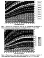
- bottom antireflective coatings are subject to interference effects which cause a periodic variation in the intensity of the reflected light with increasing thickness of the layer. Since a bottom ARC is much more absorbing than a photoresist, the bottom ARC "swing curve" is, however, severely damped. All reflection transmission factors and the phase coefficient are complex numbers. The calculation therefore quickly becomes rather messy and yields quite cumbersome expressions; we have chosen to carry it out with the symbolic algebra package of the Mathematica program (copyright Wolfram Technologies, Inc.), or with a Microsoft® ExcelTM spreadsheet written using the complex number handling provided by the ExcelTM analysis toolpack. When interpreting the reflectance values of Fig. 1, it should be kept in mind that the swing ratios are proportional to the square root of the reflectance, not to the reflectance itself
- n r For the commonly used diazonaphthoquinone/novolak g- and i-line materials, frequently encountered values of n r are 1.64 to 1.69 at 435 nm, and 1.66 to 1.72 at 365 nm.
- EP-A1- 0 583 205 discloses the use of polymeric dyes for antireflective coatings.
- the present invention covers a process for forming an image on a substrate, comprising forming an antireflective film on a substrate, where the antireflective film has a real part of refractive index optically matched to a real part of refractive index of a photoresist film coated on top of the antireflective film, and where the antireflective film contains an absorbing dye
- the antireflective film can be heated from about 70°C to about 220°C, after coating and prior to forming the photoresist film.
- the photoresist film can le heated from about 70°C to about 170°C.
- the coated substrate is heated from a temperature of from about 90°C to about 150°C for from about 30 seconds to about 180 seconds on a hot plate or from about 15 minutes to about 40 minutes in an oven after the exposure step but before the developing step.
- the coated substrate is heated at a temperature of from about 90°C to about 150°C for about 30 second to about 180 seconds on a hot plate or for from about 15 minutes to about 40 minutes in an oven after the developing step.
- the developing can be in an aqueous alkaline solution, preferably in an aqueous solution of tetramethylammonium hydroxide.
- Dispersion relations for the real part of the refractive index fail for wavelengths in or close to a region of strong absorbance.
- the reason for this is the phenomenon of anomalous dispersion, in which the real part of the refractive index is influenced by the imaginary part.
- a schematic of anomalous dispersion is shown in Fig. 2. As can be seen, in the wavelength region below the absorbance maximum, the refractive index shows a decrease, the size of which is correlated to the strength of the absorption.
- any value of the real part of the refractive index can be reached by using anomalous dispersion: it may be raised above 40 or even lowered below the value of 1 for extremely absorbing substances (e.g, for cadmium sulfide around 250 cm -1 ).
- ⁇ values will be limited to a maximum of 12 to 14 ⁇ m -1 .
- a measurement of the dispersion curve of AZ®BARLiTM coating by spectroscopic ellipsometry showed that the total change of the real part of the refractive index n ( ⁇ +) - n ( ⁇ .) (cf. Fig. 3) was about 0.32, resulting in a refractive index of 1.653 at i-line.
- the extrapolation of the Cauchy correlation to the i-line wavelength predicted a value of 1.9.
- the photoresist film comprises a diazonaphthoquinone photoactive compound and a novolak resin, and the real part of the refractive index of the antireflective film is in the range of about 1.6 to about 1.8 for an exposure wavelength of about 365 nm .
- the photoresist film comprises a diazonaphthoquinone photoactive compound and a novolak resin, and the real part of the refractive index of the antireflective film is in the range of about 1.55 to about 1.75 for an exposure wavelength of about 435 nm.
- the substrate comprises one or more components selected from the group consisting of silicon, aluminum, polymeric resins, silicon dioxide, doped silicon dioxide, silicon nitride, tantalum, copper, polysilicon, ceramics, aluminum/copper mixtures, gallium arsenide and Group III/V compounds.
- the optical lithography simulation program PROLITH Version 4.05 (a product of Finle Corporation, Austin, Texas) was used to calculate the reflectivity off a bottom coat into a photoresist.
- the reflectivity R was calculated as a function of three variables, the bottom coat thickness t in the range of zero to 350 nm in steps of 5 nm, and of the real and imaginary parts of the bottom coat refractive index n b and k b , between the values of 1.2 and 2.0 for n and 0 and 0.6 for k , both in steps of 0.05.
- n b n b , 0 to 0.6
- R(t , n b , 0 to 0.6) the optimum film thicknesses at which the swing ratio is minimized.
- Such higher thickness may be used to planarize high topography on semiconductor devices, or they may occur in deep trenches on such devices even when using lower overall coated film thickness.
- such a value of the real part of the refractive index can be obtained by careful selection of the position and width of the bottom coating's absorption bands.
Landscapes
- Engineering & Computer Science (AREA)
- Architecture (AREA)
- Structural Engineering (AREA)
- Physics & Mathematics (AREA)
- General Physics & Mathematics (AREA)
- Exposure Of Semiconductors, Excluding Electron Or Ion Beam Exposure (AREA)
- Materials For Photolithography (AREA)
- Exposure And Positioning Against Photoresist Photosensitive Materials (AREA)
Claims (10)
- Procédé pour former une image sur un substrat, consistant :a) à former un film antireflet sur un substrat, où le film antireflet a une partie réelle de l'indice de réfraction coïncidant optiquement avec la partie réelle de l'indice de réfraction du film de photorésist déposé au-dessus du film antireflet ; et où le film antireflet contient un colorant absorbant;i) où le maximum d'absorption du film antireflet est sur le côté des longueurs d'ondes inférieures des longueurs d'ondes d'exposition, ou bienii) où le maximum d'absorption du film antireflet est sur le côté supérieur des longueurs d'ondes d'exposition,b) à former un film de photorésist au-dessus du film antireflet ;c) à exposer selon une image le photorésist ;d) à développer pour former une image ;e) éventuellement, à cuire avant ou après le développement.
- Procédé selon la revendication 1, dans lequel le film de photorésist comprend un composé diazonaphtoquinone photoactif et une résine novolaque, et dans lequel la partie réelle de l'indice de réfraction du film àntireflet est dans la gamme d'environ 1,6 à environ 1,8 pour une longueur d'onde d'exposition d'environ 365 nm.
- Procédé selon la revendication 1, dans lequel le film de photorésist comprend un composé diazonaphtoquinone photoactif et une résine novolaque, et dans lequel la partie réelle de l'indice de réfraction du film antireflet est dans la gamme d'environ 1,55 à environ 1,75 pour une longueur d'onde d'exposition d'environ 435 nm.
- Procédé selon la revendication 1, comprenant de plus le chauffage du film antireflet à une température allant d'environ 70°C à environ 220°C, après le revêtement et avant la formation du film de photorésist.
- Procédé selon la revendication 1, comprenant de plus le chauffage du film de photorésist à une température d'environ 70°C à environ 170°C.
- Procédé selon la revendication 1, comprenant de plus le chauffage dudit substrat revêtu à une température allant d'environ 90°C à environ 150°C, pendant une durée d'environ 30 secondes à 180 secondes sur une plaque chaude ou pendant une durée d'environ 15 minutes à 40 minutes dans un four après l'étape d'exposition mais avant l'étape de développement.
- Procédé selon la revendication 1, comprenant de plus le chauffage dudit substrat revêtu à une température allant d'environ 90°C à environ 150°C pendant une durée d'environ 30 secondes à 180 secondes sur une plaque chaude ou pendant une durée d'environ 15 minutes à 40 minutes dans un four après l'étape de développement.
- Procédé selon la revendication 1, dans lequel ledit substrat comprend un ou plusieurs composants choisis dans le groupe comprenant le silicium, l'aluminium, les résines polymères, le dioxyde de silicium, le dioxyde de silicium dopé, le nitrure de silicium, le tantale, le cuivre, le polysilicium, les céramiques, les mélanges d'aluminium et de cuivre, l'arséniure de gallium et les composés des Groupes III/V.
- Procédé selon la revendication 1, dans lequel le développement est effectué dans une solution basique aqueuse.
- Procédé selon revendication 1, dans lequel le développement est effectué dans une solution aqueuse d'hydroxyde de tétraméthylammonium.
Applications Claiming Priority (3)
| Application Number | Priority Date | Filing Date | Title |
|---|---|---|---|
| US1300996P | 1996-03-07 | 1996-03-07 | |
| US13009P | 1996-03-07 | ||
| PCT/US1997/003835 WO1997033201A1 (fr) | 1996-03-07 | 1997-03-06 | Obtention de couches de fond antireflet par modification de l'indice de refraction grace a la dispersion anormale |
Publications (2)
| Publication Number | Publication Date |
|---|---|
| EP0885407A1 EP0885407A1 (fr) | 1998-12-23 |
| EP0885407B1 true EP0885407B1 (fr) | 2001-08-22 |
Family
ID=21757845
Family Applications (1)
| Application Number | Title | Priority Date | Filing Date |
|---|---|---|---|
| EP97915003A Expired - Lifetime EP0885407B1 (fr) | 1996-03-07 | 1997-03-06 | Obtention de couches de fond antireflet par modification de l'indice de refraction grace a la dispersion anormale |
Country Status (8)
| Country | Link |
|---|---|
| US (1) | US6042992A (fr) |
| EP (1) | EP0885407B1 (fr) |
| JP (2) | JP3877776B2 (fr) |
| KR (1) | KR100500499B1 (fr) |
| CN (1) | CN1130601C (fr) |
| DE (1) | DE69706288T2 (fr) |
| TW (1) | TW394850B (fr) |
| WO (1) | WO1997033201A1 (fr) |
Families Citing this family (15)
| Publication number | Priority date | Publication date | Assignee | Title |
|---|---|---|---|---|
| US5733714A (en) * | 1996-09-30 | 1998-03-31 | Clariant Finance (Bvi) Limited | Antireflective coating for photoresist compositions |
| US6274295B1 (en) * | 1997-03-06 | 2001-08-14 | Clariant Finance (Bvi) Limited | Light-absorbing antireflective layers with improved performance due to refractive index optimization |
| US5981145A (en) * | 1997-04-30 | 1999-11-09 | Clariant Finance (Bvi) Limited | Light absorbing polymers |
| US5994430A (en) * | 1997-04-30 | 1999-11-30 | Clariant Finance Bvi) Limited | Antireflective coating compositions for photoresist compositions and use thereof |
| EP1016930A1 (fr) * | 1998-12-28 | 2000-07-05 | Infineon Technologies North America Corp. | Couche de base antiréfléchissante avec interférences destructives et propriétés absorbantes |
| US6599682B2 (en) * | 2000-04-26 | 2003-07-29 | Tokyo Ohka Kogyo Co., Ltd. | Method for forming a finely patterned photoresist layer |
| US7070914B2 (en) * | 2002-01-09 | 2006-07-04 | Az Electronic Materials Usa Corp. | Process for producing an image using a first minimum bottom antireflective coating composition |
| US7009750B1 (en) | 2002-10-25 | 2006-03-07 | Eclipse Energy Systems, Inc. | Apparatus and methods for modulating refractive index |
| DE602006017047D1 (de) * | 2006-06-14 | 2010-11-04 | Eastman Kodak Co | Verfahren zur Verarbeitung von Fotopolymer-Druckplatten, die eine Deckschicht enthalten |
| US7416834B2 (en) * | 2006-09-27 | 2008-08-26 | Az Electronic Materials Usa Corp. | Antireflective coating compositions |
| US8221965B2 (en) * | 2008-07-08 | 2012-07-17 | Az Electronic Materials Usa Corp. | Antireflective coating compositions |
| US8329387B2 (en) * | 2008-07-08 | 2012-12-11 | Az Electronic Materials Usa Corp. | Antireflective coating compositions |
| US20100092894A1 (en) * | 2008-10-14 | 2010-04-15 | Weihong Liu | Bottom Antireflective Coating Compositions |
| US8507192B2 (en) * | 2010-02-18 | 2013-08-13 | Az Electronic Materials Usa Corp. | Antireflective compositions and methods of using same |
| US9170494B2 (en) | 2012-06-19 | 2015-10-27 | Az Electronic Materials (Luxembourg) S.A.R.L. | Antireflective compositions and methods of using same |
Family Cites Families (25)
| Publication number | Priority date | Publication date | Assignee | Title |
|---|---|---|---|---|
| JPS5851515A (ja) * | 1981-09-22 | 1983-03-26 | Fujitsu Ltd | レジスト膜の露光方法 |
| DE3211400A1 (de) * | 1982-03-27 | 1983-09-29 | Basf Ag, 6700 Ludwigshafen | Polymere mit mesogenen gruppen und farbstoffresten in den seitenketten |
| US4491628A (en) * | 1982-08-23 | 1985-01-01 | International Business Machines Corporation | Positive- and negative-working resist compositions with acid generating photoinitiator and polymer with acid labile groups pendant from polymer backbone |
| US5207952A (en) * | 1986-10-10 | 1993-05-04 | University Of Southern Mississippi | Side chain liquid crystalline polymers as nonlinear optical materials |
| JPS63202915A (ja) * | 1987-02-19 | 1988-08-22 | Oki Electric Ind Co Ltd | 半導体装置の製造方法 |
| DE3817012A1 (de) * | 1988-05-19 | 1989-11-30 | Basf Ag | Positiv und negativ arbeitende strahlungsempfindliche gemische sowie verfahren zur herstellung von reliefmustern |
| DE69125634T2 (de) * | 1990-01-30 | 1998-01-02 | Wako Pure Chem Ind Ltd | Chemisch verstärktes Photolack-Material |
| FR2668158B1 (fr) * | 1990-10-22 | 1994-05-06 | Thomson Csf | Polymere reticulable pour applications en optique non lineaire. |
| EP0522990B1 (fr) * | 1991-06-28 | 1996-09-25 | International Business Machines Corporation | Films superficiels antiréfléchissants |
| US5472827A (en) * | 1991-12-30 | 1995-12-05 | Sony Corporation | Method of forming a resist pattern using an anti-reflective layer |
| JP2791525B2 (ja) * | 1992-04-16 | 1998-08-27 | 三菱電機株式会社 | 反射防止膜の選定方法およびその方法により選定された反射防止膜 |
| US5294680A (en) * | 1992-07-24 | 1994-03-15 | International Business Machines Corporation | Polymeric dyes for antireflective coatings |
| JP2829555B2 (ja) * | 1992-08-20 | 1998-11-25 | 三菱電機株式会社 | 微細レジストパターンの形成方法 |
| DE4232394A1 (de) * | 1992-09-26 | 1994-03-31 | Basf Ag | Copolymerisate mit nichtlinear optischen Eigenschaften und deren Verwendung |
| SG49596A1 (en) * | 1992-11-25 | 1998-06-15 | Hoechst Celanese Corp | Metal ion reduction in bottom anti-reflective coatings for photoresists |
| KR100188508B1 (ko) * | 1993-03-26 | 1999-06-01 | 세끼사와 다까시 | 비정질탄소막을 사용하는 패턴형성방법과 에칭방법 및 비정질탄소막 형성방법 |
| FR2709755B1 (fr) * | 1993-09-06 | 1995-11-17 | France Telecom | Matériau polymère réticulable, utilisable en optique non linéaire, et son procédé d'obtention. |
| DE69423641T2 (de) * | 1993-10-12 | 2000-10-19 | Clariant Finance (Bvi) Ltd., Road Town | Reflexionsvermindernde oberflächenbeschichtungen |
| JP3334304B2 (ja) * | 1993-11-30 | 2002-10-15 | ソニー株式会社 | 半導体装置の製造方法 |
| KR100366910B1 (ko) * | 1994-04-05 | 2003-03-04 | 소니 가부시끼 가이샤 | 반도체장치의제조방법 |
| JP3248353B2 (ja) * | 1994-06-29 | 2002-01-21 | ソニー株式会社 | 反射防止膜の設計方法 |
| US5525457A (en) * | 1994-12-09 | 1996-06-11 | Japan Synthetic Rubber Co., Ltd. | Reflection preventing film and process for forming resist pattern using the same |
| KR100458685B1 (ko) * | 1996-03-07 | 2005-06-02 | 클라리언트 인터내셔널 리미티드 | 굴절율을최적화함으로써개선된성능을갖는광흡수성반사방지층 |
| US5652297A (en) * | 1996-08-16 | 1997-07-29 | Hoechst Celanese Corporation | Aqueous antireflective coatings for photoresist compositions |
| US5652317A (en) * | 1996-08-16 | 1997-07-29 | Hoechst Celanese Corporation | Antireflective coatings for photoresist compositions |
-
1997
- 1997-03-06 KR KR10-1998-0706195A patent/KR100500499B1/ko not_active Expired - Fee Related
- 1997-03-06 DE DE69706288T patent/DE69706288T2/de not_active Expired - Lifetime
- 1997-03-06 TW TW086102746A patent/TW394850B/zh not_active IP Right Cessation
- 1997-03-06 EP EP97915003A patent/EP0885407B1/fr not_active Expired - Lifetime
- 1997-03-06 CN CN97192868A patent/CN1130601C/zh not_active Expired - Lifetime
- 1997-03-06 JP JP53200997A patent/JP3877776B2/ja not_active Expired - Fee Related
- 1997-03-06 US US08/811,806 patent/US6042992A/en not_active Expired - Lifetime
- 1997-03-06 WO PCT/US1997/003835 patent/WO1997033201A1/fr not_active Ceased
-
2006
- 2006-05-08 JP JP2006129460A patent/JP4044118B2/ja not_active Expired - Fee Related
Also Published As
| Publication number | Publication date |
|---|---|
| JP3877776B2 (ja) | 2007-02-07 |
| KR19990082462A (ko) | 1999-11-25 |
| JP4044118B2 (ja) | 2008-02-06 |
| CN1130601C (zh) | 2003-12-10 |
| TW394850B (en) | 2000-06-21 |
| JP2000506288A (ja) | 2000-05-23 |
| CN1213437A (zh) | 1999-04-07 |
| EP0885407A1 (fr) | 1998-12-23 |
| DE69706288D1 (de) | 2001-09-27 |
| KR100500499B1 (ko) | 2005-12-30 |
| US6042992A (en) | 2000-03-28 |
| WO1997033201A1 (fr) | 1997-09-12 |
| JP2006287243A (ja) | 2006-10-19 |
| DE69706288T2 (de) | 2002-05-16 |
Similar Documents
| Publication | Publication Date | Title |
|---|---|---|
| EP0885407B1 (fr) | Obtention de couches de fond antireflet par modification de l'indice de refraction grace a la dispersion anormale | |
| US6274295B1 (en) | Light-absorbing antireflective layers with improved performance due to refractive index optimization | |
| Brunner et al. | High-NA lithographic imagery at Brewster's angle | |
| JP2010107996A (ja) | 屈折率を最適化して性能を改善した光吸収性の反射防止層 | |
| KR20040009191A (ko) | 반도체 소자의 패턴 형성 방법 | |
| Miura et al. | Reduction of linewidth variation over reflective topography | |
| Dammel et al. | Modeling of bottom antireflection layers: sensitivity to optical constants | |
| Flagello et al. | High-numerical-aperture effects in photoresist | |
| TW200525141A (en) | Defect inspection device and defect inspection method | |
| JP2003507760A (ja) | フォトレジスト用の反射防止膜用組成物 | |
| Ogawa et al. | Novel ARC optimization methodology for KrF excimer laser lithography at low K1 factor | |
| EP0154932A2 (fr) | Procédé photolaque à plusieurs couches | |
| Kuyel et al. | The effects of broadband 250 nm illumination on process latitude | |
| Dunn et al. | Deep-UV photolithography linewidth variation from reflective substrates | |
| JPH1131650A (ja) | 反射防止膜、被処理基板、被処理基板の製造方法、微細パターンの製造方法、および半導体装置の製造方法 | |
| Mack | Lithography on reflective substrates | |
| Goldfarb et al. | Graded spin-on organic bottom antireflective coating for high NA lithography | |
| Pavelchek | Tunable AR for DUV lithography | |
| Vloeberghs et al. | Influence of substrate reflectivity on linewidth control | |
| Meador et al. | Improved crosslinkable polymeric binders for 193-nm bottom antireflective coatings (BARCs) | |
| Dumford et al. | The Ag/As2S3 photodoping mechanism: photon absorption | |
| Nagata et al. | Characterization of thin-film interference effect due to surface roughness | |
| Okoroanyanwu et al. | Impact of optical absorption on process control for sub-0.15-nm device patterning using 193-nm lithography | |
| Hilfiker et al. | Metrology applications in lithography with variable angle spectroscopic ellipsometry | |
| Kennedy et al. | High Si content BARC for applications in dual BARC systems such as tri-layer patterning |
Legal Events
| Date | Code | Title | Description |
|---|---|---|---|
| PUAI | Public reference made under article 153(3) epc to a published international application that has entered the european phase |
Free format text: ORIGINAL CODE: 0009012 |
|
| 17P | Request for examination filed |
Effective date: 19981007 |
|
| AK | Designated contracting states |
Kind code of ref document: A1 Designated state(s): DE FR GB IT |
|
| RAP1 | Party data changed (applicant data changed or rights of an application transferred) |
Owner name: CLARIANT FINANCE (BVI) LIMITED |
|
| 17Q | First examination report despatched |
Effective date: 19991216 |
|
| GRAG | Despatch of communication of intention to grant |
Free format text: ORIGINAL CODE: EPIDOS AGRA |
|
| GRAG | Despatch of communication of intention to grant |
Free format text: ORIGINAL CODE: EPIDOS AGRA |
|
| GRAH | Despatch of communication of intention to grant a patent |
Free format text: ORIGINAL CODE: EPIDOS IGRA |
|
| GRAH | Despatch of communication of intention to grant a patent |
Free format text: ORIGINAL CODE: EPIDOS IGRA |
|
| GRAA | (expected) grant |
Free format text: ORIGINAL CODE: 0009210 |
|
| AK | Designated contracting states |
Kind code of ref document: B1 Designated state(s): DE FR GB IT |
|
| REF | Corresponds to: |
Ref document number: 69706288 Country of ref document: DE Date of ref document: 20010927 |
|
| REG | Reference to a national code |
Ref country code: GB Ref legal event code: IF02 |
|
| ET | Fr: translation filed | ||
| PLBE | No opposition filed within time limit |
Free format text: ORIGINAL CODE: 0009261 |
|
| STAA | Information on the status of an ep patent application or granted ep patent |
Free format text: STATUS: NO OPPOSITION FILED WITHIN TIME LIMIT |
|
| 26N | No opposition filed | ||
| REG | Reference to a national code |
Ref country code: GB Ref legal event code: 732E |
|
| REG | Reference to a national code |
Ref country code: FR Ref legal event code: TP |
|
| PGFP | Annual fee paid to national office [announced via postgrant information from national office to epo] |
Ref country code: GB Payment date: 20080211 Year of fee payment: 12 |
|
| GBPC | Gb: european patent ceased through non-payment of renewal fee |
Effective date: 20090306 |
|
| PG25 | Lapsed in a contracting state [announced via postgrant information from national office to epo] |
Ref country code: GB Free format text: LAPSE BECAUSE OF NON-PAYMENT OF DUE FEES Effective date: 20090306 |
|
| REG | Reference to a national code |
Ref country code: DE Ref legal event code: R082 Ref document number: 69706288 Country of ref document: DE Representative=s name: PATENTANWAELTE ISENBRUCK BOESL HOERSCHLER LLP, DE |
|
| REG | Reference to a national code |
Ref country code: FR Ref legal event code: PLFP Year of fee payment: 19 |
|
| REG | Reference to a national code |
Ref country code: FR Ref legal event code: TP Owner name: MERCK PATENT GMBH, DE Effective date: 20150204 |
|
| REG | Reference to a national code |
Ref country code: DE Ref legal event code: R082 Ref document number: 69706288 Country of ref document: DE Representative=s name: PATENTANWAELTE ISENBRUCK BOESL HOERSCHLER LLP, DE Effective date: 20150223 Ref country code: DE Ref legal event code: R081 Ref document number: 69706288 Country of ref document: DE Owner name: MERCK PATENT GMBH, DE Free format text: FORMER OWNER: AZ ELECTRONIC MATERIALS USA CORP. (N.D.GES.D. STAATES DELAWARE), SOMERVILLE, N.J., US Effective date: 20150223 |
|
| REG | Reference to a national code |
Ref country code: FR Ref legal event code: PLFP Year of fee payment: 20 |
|
| PGFP | Annual fee paid to national office [announced via postgrant information from national office to epo] |
Ref country code: IT Payment date: 20160311 Year of fee payment: 20 |
|
| PGFP | Annual fee paid to national office [announced via postgrant information from national office to epo] |
Ref country code: FR Payment date: 20160223 Year of fee payment: 20 |
|
| PGFP | Annual fee paid to national office [announced via postgrant information from national office to epo] |
Ref country code: DE Payment date: 20160324 Year of fee payment: 20 |
|
| REG | Reference to a national code |
Ref country code: DE Ref legal event code: R071 Ref document number: 69706288 Country of ref document: DE |