EP0885455B1 - Vorrichtung zur erzeugung von leistungsfähigen mikrowellenplasmen - Google Patents
Vorrichtung zur erzeugung von leistungsfähigen mikrowellenplasmen Download PDFInfo
- Publication number
- EP0885455B1 EP0885455B1 EP97906173A EP97906173A EP0885455B1 EP 0885455 B1 EP0885455 B1 EP 0885455B1 EP 97906173 A EP97906173 A EP 97906173A EP 97906173 A EP97906173 A EP 97906173A EP 0885455 B1 EP0885455 B1 EP 0885455B1
- Authority
- EP
- European Patent Office
- Prior art keywords
- resonator
- plasma chamber
- coaxial
- chamber
- coupling points
- Prior art date
- Legal status (The legal status is an assumption and is not a legal conclusion. Google has not performed a legal analysis and makes no representation as to the accuracy of the status listed.)
- Expired - Lifetime
Links
- 210000002381 plasma Anatomy 0.000 title claims abstract description 43
- 239000004020 conductor Substances 0.000 claims abstract description 17
- 238000004519 manufacturing process Methods 0.000 claims abstract description 4
- 230000008878 coupling Effects 0.000 claims description 18
- 238000010168 coupling process Methods 0.000 claims description 18
- 238000005859 coupling reaction Methods 0.000 claims description 18
- 230000015572 biosynthetic process Effects 0.000 description 2
- 239000003989 dielectric material Substances 0.000 description 2
- 239000007789 gas Substances 0.000 description 2
- 239000002184 metal Substances 0.000 description 2
- VYPSYNLAJGMNEJ-UHFFFAOYSA-N Silicium dioxide Chemical compound O=[Si]=O VYPSYNLAJGMNEJ-UHFFFAOYSA-N 0.000 description 1
- 239000004809 Teflon Substances 0.000 description 1
- 229920006362 Teflon® Polymers 0.000 description 1
- 239000000919 ceramic Substances 0.000 description 1
- 238000004140 cleaning Methods 0.000 description 1
- 239000011248 coating agent Substances 0.000 description 1
- 238000000576 coating method Methods 0.000 description 1
- 238000000354 decomposition reaction Methods 0.000 description 1
- 238000009826 distribution Methods 0.000 description 1
- 239000004744 fabric Substances 0.000 description 1
- 239000000463 material Substances 0.000 description 1
- 238000000034 method Methods 0.000 description 1
- 238000004377 microelectronic Methods 0.000 description 1
- 239000007787 solid Substances 0.000 description 1
- 238000003786 synthesis reaction Methods 0.000 description 1
Images


Classifications
-
- H—ELECTRICITY
- H01—ELECTRIC ELEMENTS
- H01J—ELECTRIC DISCHARGE TUBES OR DISCHARGE LAMPS
- H01J37/00—Discharge tubes with provision for introducing objects or material to be exposed to the discharge, e.g. for the purpose of examination or processing thereof
- H01J37/32—Gas-filled discharge tubes
- H01J37/32009—Arrangements for generation of plasma specially adapted for examination or treatment of objects, e.g. plasma sources
- H01J37/32192—Microwave generated discharge
- H01J37/32211—Means for coupling power to the plasma
- H01J37/32247—Resonators
-
- H—ELECTRICITY
- H01—ELECTRIC ELEMENTS
- H01J—ELECTRIC DISCHARGE TUBES OR DISCHARGE LAMPS
- H01J37/00—Discharge tubes with provision for introducing objects or material to be exposed to the discharge, e.g. for the purpose of examination or processing thereof
- H01J37/32—Gas-filled discharge tubes
- H01J37/32009—Arrangements for generation of plasma specially adapted for examination or treatment of objects, e.g. plasma sources
- H01J37/32192—Microwave generated discharge
-
- H—ELECTRICITY
- H05—ELECTRIC TECHNIQUES NOT OTHERWISE PROVIDED FOR
- H05H—PLASMA TECHNIQUE; PRODUCTION OF ACCELERATED ELECTRICALLY-CHARGED PARTICLES OR OF NEUTRONS; PRODUCTION OR ACCELERATION OF NEUTRAL MOLECULAR OR ATOMIC BEAMS
- H05H1/00—Generating plasma; Handling plasma
- H05H1/24—Generating plasma
- H05H1/46—Generating plasma using applied electromagnetic fields, e.g. high frequency or microwave energy
-
- H—ELECTRICITY
- H01—ELECTRIC ELEMENTS
- H01J—ELECTRIC DISCHARGE TUBES OR DISCHARGE LAMPS
- H01J37/00—Discharge tubes with provision for introducing objects or material to be exposed to the discharge, e.g. for the purpose of examination or processing thereof
- H01J37/32—Gas-filled discharge tubes
- H01J37/32431—Constructional details of the reactor
- H01J37/32733—Means for moving the material to be treated
- H01J37/32743—Means for moving the material to be treated for introducing the material into processing chamber
Definitions
- Microwave plasmas are used in technical areas such as e.g. the manufacture or processing of components, in microelectronics, in coating, in gas decomposition, fabric synthesis or material cleaning used.
- the microwaves are in the plasma chamber with the recipient, if any, located therein, i.e. Usable space, from a microwave generator, if necessary, via a Lead to a waveguide resonator around the plasma chamber passed through coupling points.
- a waveguide resonator around the plasma chamber passed through coupling points.
- special Ring resonators i.e. ring-shaped waveguide resonators with little length along its axis, compared to the relatively large diameter of the cross section of the resonator ring.
- the axis of the Ring resonator and the axis of the e.g. as Pipe formed plasma chamber the same or a common one z-axis.
- the resonator ring has one rectangular cross section and the coupling points e.g. as slots in the short cross-sectional side.
- Such Have devices for generating microwave plasmas good effectiveness.
- the invention relates to a device for generating of microwave plasmas, the resonator of which is a coaxial resonator is formed with inner and outer conductors, according to claim 1. So far Head all or part of the interior and exterior boundaries of the resonator is their shape and Any shape of the ladder. Both leaders preferred a similar, similar, or same axis direction or a common axis z. Vacuum is the Surprisingly, the device is not absolutely necessary.
- a device according to claim 1, preamble, is known from EP-A-564359.
- the production is made of hollow profiles, preferably e.g. Rolled profiles, elongated type, used as a coaxial conductor are arranged one inside the other and completed at the ends or can be open. Examples that are easy to design two pipes or cylinders are arbitrary, even angular Base area that are arranged one inside the other. A wire or solid cylinder as inner conductor is preferred, if only coupling via the outer conductor.
- the resonator can be in substantially the same axis z-direction like the plasma chamber and own resonator and plasma chamber can be the same along the z-direction long or not the same length.
- the invention therefore starts from the narrow resonator ring with different cross-sections, the plasma chamber, e.g. is designed as a resonator, such as a Finger ring encompasses the finger of one hand.
- the coaxial resonator according to the invention is elongated and can e.g. as a cover like the space of a finger cover of the Glove around the finger along essentially the entire length be formed in the direction of the z-axis.
- plasma chamber and resonator are not according to the invention to a specific one Shape of the hollow body bound.
- the inner and outer conductor the coaxial resonator very preferably has essentially with its long or longest axis z axis, essentially the same direction. Prefers is the same direction of the axes of the chamber and the coaxial resonator, a common or parallel axis, however is also a small angle or a tilt possible up to 90 ° between the axes of both components.
- Coaxial conductors made of flexible metal hoses e.g. as spiral strips or interlocking Rings are possible, with two arranged one inside the other Hoses or a hose converted to e.g. a tubular or egg-shaped chamber than the one ladder, form the resonator.
- the wall of the plasma chamber can be a ladder, the shape of the plasma chamber being arbitrary is, but constant training as a tube, ball or cylinder are preferred.
- the chamber and resonator can be the same or be of unequal length, with one or more chambers, one or more coaxial resonators or divided chambers or coaxial resonators e.g. perpendicular to the preferred direction can be trained.
- Coupling points as e.g. Antennas or preferably as Slots or recesses can be on the walls of the Coaxial resonators, i.e. to those in common with the Chamber Walls, in any number, preferably in that for the each selected plasma mode required number, geometry and arrangement.
- Coupling points of small dimensions disturb the resonance not essential in the coaxial resonator. Such coupling points and enable a larger number of coupling points the often preferred homogeneous formation of the plasma in the plasma chamber and a resonance in the chamber in If suitable dimensions.
- the microwave source can be controlled directly, if necessary Supply line or via another resonator at any Location of the coaxial resonator, also at the inner boundary, be arranged and in one or more Couple the plasma chambers.
- the plasma chamber as well as the Coaxial resonator can be completely or partially a dielectric Material such as Ceramic, quartz glass or teflon contain.
- An inner chamber arranged wholly or partially in the inner conductor is also possible an outer chamber and possibly both one or more outer chambers and one or more Inner chambers, each with a usable space or Recipients with dielectric walls of any Shape.
- the coaxial resonator of the invention thus enables one Diversity of shape and training.
- the plasma chamber can be an additional resonator or its part.
- the plasma chamber is preferably designed as cylinder resonator and the associated training certain Fashions.
- Several supply lines for the microwaves one or more coaxial resonators can be formed his.
- the preferred coaxial modes TEM or TM n1 are optimally formed in the coaxial resonator between two preferably cylindrical, electrically conductive tubes of different diameters. Any TE nm or TM nm field distributions are also possible.
- the length of both tubes is preferably a multiple of half the line wavelength of the microwave used.
- the pipes are then electrically conductively delimited at both ends, for example by a wall, gas-permeable grid or a short-circuit slide.
- the recipient (s), as usual from dielectric Material, according to the invention can be large-volume and serve different tasks in the case of division.
- a large-scale recipient arranged outside is a metallic one End wall not absolutely necessary.
- Permanent magnets or coil arrangements e.g. according to Helmholz around the outer tube or the metal outer wall allow the conditions for electrons in the chamber Cyclotron resonance plasmas.
- An arrangement of magnets is in the inner conductor of the coaxial resonator as well possible.
- FIG. 1 shows a section through a device in FIG along the z-axis, Fig. 1b, the associated supervision.
- a device with an inner wall 2 is shown and outer wall 3 of a tubular coaxial resonator Microwave source 4, which is in the resonator between 2 and 3 couples, and recipients 1.
- Fig.1 are two coupling slots 5 as circumferential slots in the inner wall 2 performed; these are thus perpendicular to the z-axis of the Contraption.
- Coaxial resonator and internal plasma chamber which is designed as a cylindrical resonator in this embodiment, the same length in the z direction. 10 is an optional e.g. metallic grid, which divides the plasma chamber into two chambers.
- Figure 2 shows a device similar to Figure 1, however here are the coupling points 5 as longitudinal slots in the Wall of the inner coaxial conductor arranged and run thus parallel to the z-axis of the device.
- Farther are some tuning options of coaxial resonator in Fig. 2 and plasma chamber listed as examples.
- the Termination slide 7 is used to tune the coaxial resonator.
- the tuning pin or screw 8 serves that same purpose.
- the location and number of such voting elements can be varied as required.
- the voting pen 9 shows a possibility of tuning the plasma chamber.
- a a closing slide, not shown here, has a similar function, which changes the length of the plasma chamber.
- the arrows in the figure indicate the direction of movement of the Voting elements.
- the microwave generator 4 is inside the Inner conductor 2 of the coaxial resonator attached.
- the Coupling points 5 are three azimuthal, partially rotating Coupling slots in the outer wall of the coaxial resonator executed.
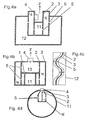
- FIG. 4 shows further exemplary embodiments of the device outlined, in Fig. 4a a section through a device with both the inner plasma chamber 11 and the outer one Chamber 12 is shown. If necessary, you can the plasma chambers 11, 12 are equipped with recipients become.
- Fig. 4b shows a section through a device, at the microwave in a cylinder resonator 13 directly is coupled and this resonator over a rotating azimuthal slots coupled to the coaxial resonator is.
- the coupling into the as another cylinder resonator trained plasma chamber 11 with recipient 1 takes place via further coupling slots.
- FIG. 4c shows a section through a device in which a e.g. helically coiled resonator with outer conductor 3 and similarly coiled e.g. as Wire-formed inner conductor 2 in a cylindrical Chamber 12 is located.
- a e.g. helically coiled resonator with outer conductor 3 and similarly coiled e.g. as Wire-formed inner conductor 2 in a cylindrical Chamber 12 is located.
- a design in which the coaxial resonator in a coiled or coiled form with the outer conductor completely or partially encloses a chamber, i.e. as e.g. a band or a cord wrapped around a chamber is also possible.
- the 4d shows a section through a device with spherical plasma chamber 11.
- the antenna of the microwave generator 4 is directly connected to the inner conductor 2 of the coaxial resonator connected.
- the outer conductor 3 is for Microwave generator 4 tapers conically.
- About one azimuthal coupling slot 5 is the microwave power coupled into the plasma chamber.
Landscapes
- Physics & Mathematics (AREA)
- Engineering & Computer Science (AREA)
- Plasma & Fusion (AREA)
- Chemical & Material Sciences (AREA)
- Analytical Chemistry (AREA)
- Electromagnetism (AREA)
- Spectroscopy & Molecular Physics (AREA)
- Plasma Technology (AREA)
- Chemical Vapour Deposition (AREA)
- Electron Sources, Ion Sources (AREA)
- Drying Of Semiconductors (AREA)
- Manufacture And Refinement Of Metals (AREA)
Description
Claims (8)
- Vorrichtung zur Erzeugung von Mikrowellenplasmen, die mindestens einen Mikrowellenerzeuger (4), mindestens einen zuleitenden Resonator (15), mindestens eine Plasmakammer (11,12) und Koppelstellen (5) zwischen zuleitendem Resonator (15) und Plasmakammer (11,12) umfaßt, dadurch gekennzeichnet, daß Außenabgrenzung (3) und Innenabgrenzung (2) des zuleitenden Resonators (15) als Außen- und Innenleiter eines Koaxialresonators ausgebildet sind.
- Vorrichtung nach Anspruch 1, dadurch gekennzeichnet, daß sie einen oder mehrere Rezipienten (1) mit dielektrischen Wandungen aufweist.
- Vorrichtung nach Anspruch 1 oder 2, dadurch gekennzeichnet, daß die Plasmakammer (11) vom Resonator (15) ganz oder teilweise umfaßt ist.
- Vorrichtung nach Anspruch 1 oder 2, dadurch gekennzeichnet, daß der Resonator (15) von der Plasmakammer (12) ganz oder teilweise umfaßt ist.
- Vorrichtung nach Anspruch 1 oder 2, dadurch gekennzeichnet, daß innerhalb und/oder außerhalb des Resonators (15) eine oder mehrere Kammern angeordnet sind, bzw. daß die Plasmakammer (11,12) geteilt ist.
- Vorrichtung nach einem der vorangehenden Ansprüche, dadurch gekennzeichnet, daß der Koaxial-Resonator (15) und die Plasmakammer (11,12) die gleiche Vorzugsrichtung aufweisen und gleich lang oder verschieden lang ausgebildet sind.
- Vorrichtung nach einem der vorangehenden Ansprüche, dadurch gekennzeichnet, daß die Koppelstellen (5) für die Ein- bzw. Auskopplung der Mikrowellen von dem Resonator (15) in bzw. an den Wandungen des Koaxial-Resonators (15) bzw. in oder an der gemeinsamen Wand von Kammer (11,12) und Resonator (15) angeordnet sind.
- Vorrichtung nach einem der vorangehenden Ansprüche, dadurch gekennzeichnet, daß die Koppelstellen (5) Stabantennen oder/und Schlaufen oder/und Schlitze oder/und Aussparungen sind.
Applications Claiming Priority (3)
| Application Number | Priority Date | Filing Date | Title |
|---|---|---|---|
| DE19608949A DE19608949A1 (de) | 1996-03-08 | 1996-03-08 | Vorrichtung zur Erzeugung von leistungsfähigen Mikrowellenplasmen |
| DE19608949 | 1996-03-08 | ||
| PCT/EP1997/001114 WO1997033299A1 (de) | 1996-03-08 | 1997-03-03 | Vorrichtung zur erzeugung von leistungsfähigen mikrowellenplasmen |
Publications (2)
| Publication Number | Publication Date |
|---|---|
| EP0885455A1 EP0885455A1 (de) | 1998-12-23 |
| EP0885455B1 true EP0885455B1 (de) | 2004-07-21 |
Family
ID=7787582
Family Applications (1)
| Application Number | Title | Priority Date | Filing Date |
|---|---|---|---|
| EP97906173A Expired - Lifetime EP0885455B1 (de) | 1996-03-08 | 1997-03-03 | Vorrichtung zur erzeugung von leistungsfähigen mikrowellenplasmen |
Country Status (9)
| Country | Link |
|---|---|
| US (1) | US6204603B1 (de) |
| EP (1) | EP0885455B1 (de) |
| JP (1) | JP3571056B2 (de) |
| KR (1) | KR100458080B1 (de) |
| AT (1) | ATE271717T1 (de) |
| CA (1) | CA2248250C (de) |
| DE (2) | DE19608949A1 (de) |
| ES (1) | ES2225953T3 (de) |
| WO (1) | WO1997033299A1 (de) |
Families Citing this family (23)
| Publication number | Priority date | Publication date | Assignee | Title |
|---|---|---|---|---|
| DE19726663A1 (de) * | 1997-06-23 | 1999-01-28 | Sung Spitzl Hildegard Dr Ing | Vorrichtung zur Erzeugung von homogenen Mikrowellenplasmen |
| DE19847848C1 (de) * | 1998-10-16 | 2000-05-11 | R3 T Gmbh Rapid Reactive Radic | Vorrichtung und Erzeugung angeregter/ionisierter Teilchen in einem Plasma |
| DE19928876A1 (de) * | 1999-06-24 | 2000-12-28 | Leybold Systems Gmbh | Vorrichtung zur lokalen Erzeugung eines Plasmas in einer Behandlungskammer durch Mikrowellenanregung |
| DE10114115A1 (de) * | 2001-03-22 | 2002-10-02 | Muegge Electronic Gmbh | Anordnung zur Erzeugung von Plasma in einem Behandlungsraum |
| DE10138693A1 (de) * | 2001-08-07 | 2003-07-10 | Schott Glas | Vorrichtung zum Beschichten von Gegenständen |
| US20050212626A1 (en) * | 2002-05-07 | 2005-09-29 | Toshiyuki Takamatsu | High frequency reaction processing system |
| DE10322367A1 (de) * | 2003-05-13 | 2004-12-02 | Dreyer, Dietmar, Dipl.-Ing. (FH) | Speicherbatterie auf der Basis eines Hochfrequenzplasmas |
| DE10358329B4 (de) | 2003-12-12 | 2007-08-02 | R3T Gmbh Rapid Reactive Radicals Technology | Vorrichtung zur Erzeugung angeregter und/oder ionisierter Teilchen in einem Plasma und Verfahren zur Erzeugung ionisierter Teilchen |
| DE102006062339A1 (de) * | 2006-12-22 | 2008-07-03 | TRüTZSCHLER GMBH & CO. KG | Mikrowellenresonator für eine oder an einer Textilmaschine, insb. Karde, Strecke, Kämmmaschine o. dgl. |
| EP2101547B1 (de) * | 2008-03-11 | 2014-03-05 | Vita Zahnfabrik H. Rauter GmbH & Co. KG | Dental-Sinterofen sowie Verfahren zum Sintern keramischer Dental-Elemente |
| GB0902784D0 (en) | 2009-02-19 | 2009-04-08 | Gasplas As | Plasma reactor |
| NO339087B1 (no) | 2010-08-17 | 2016-11-14 | Gasplas As | Anordning, system og fremgangsmåte for fremstilling av hydrogen |
| DE102011051542B4 (de) * | 2011-07-04 | 2013-04-25 | Jenoptik Katasorb Gmbh | Mikrowellenreaktor zur mikrowellenunterstützten Erwärmung eines Mediums |
| DE102014016380A1 (de) | 2014-11-06 | 2016-05-12 | Brückner Maschinenbau GmbH & Co. KG | Plasma Abgasreinigung |
| US9736920B2 (en) * | 2015-02-06 | 2017-08-15 | Mks Instruments, Inc. | Apparatus and method for plasma ignition with a self-resonating device |
| US10748745B2 (en) * | 2016-08-16 | 2020-08-18 | Applied Materials, Inc. | Modular microwave plasma source |
| US10707058B2 (en) | 2017-04-11 | 2020-07-07 | Applied Materials, Inc. | Symmetric and irregular shaped plasmas using modular microwave sources |
| US11037764B2 (en) | 2017-05-06 | 2021-06-15 | Applied Materials, Inc. | Modular microwave source with local Lorentz force |
| DE102018000401A1 (de) | 2018-01-19 | 2019-07-25 | Ralf Spitzl | Mikrowellenplasmavorrichtung |
| US11081317B2 (en) | 2018-04-20 | 2021-08-03 | Applied Materials, Inc. | Modular high-frequency source |
| US11393661B2 (en) | 2018-04-20 | 2022-07-19 | Applied Materials, Inc. | Remote modular high-frequency source |
| US10504699B2 (en) | 2018-04-20 | 2019-12-10 | Applied Materials, Inc. | Phased array modular high-frequency source |
| KR102929829B1 (ko) * | 2020-03-23 | 2026-02-23 | 에스에스티 인크. | 고주파 반응 프로세싱 장치 및 고주파 반응 프로세싱 시스템 |
Family Cites Families (13)
| Publication number | Priority date | Publication date | Assignee | Title |
|---|---|---|---|---|
| US3577207A (en) * | 1969-05-07 | 1971-05-04 | Vladimir Pavlovich Kirjushin | Microwave plasmatron |
| DE1960022B2 (de) | 1969-11-29 | 1973-09-27 | Grundig E.M.V. Elektro-Mechanische Versuchsanstalt Max Grundig, 8510 Fuerth | Schaltungsanordnung zur Anzeige der Senderfeldstarke am Signaleingang eines Empfangers für Frequenzmoduherte Hochfrequente Schwingungen |
| FR2147497A5 (de) * | 1971-07-29 | 1973-03-09 | Commissariat Energie Atomique | |
| US4559099A (en) * | 1984-08-24 | 1985-12-17 | Technics Gmbh Europa | Etching device |
| FR2668676B2 (fr) * | 1986-06-06 | 1993-06-11 | Univ Bordeaux 1 | Dispositif perfectionne pour l'application de micro-ondes. |
| FR2631199B1 (fr) * | 1988-05-09 | 1991-03-15 | Centre Nat Rech Scient | Reacteur a plasma |
| US5134965A (en) * | 1989-06-16 | 1992-08-04 | Hitachi, Ltd. | Processing apparatus and method for plasma processing |
| DE4113142A1 (de) * | 1991-03-14 | 1992-09-17 | Leybold Ag | Vorrichtung zur erzeugung von glimmentladungen |
| WO2004089046A1 (ja) * | 1991-11-05 | 2004-10-14 | Nobumasa Suzuki | 無端環状導波管を有するマイクロ波導入装置及び該装置を備えたプラズマ処理装置 |
| FR2689717B1 (fr) * | 1992-04-03 | 1994-05-13 | Commissariat A Energie Atomique | Dispositif d'application de micro-ondes et reacteur a plasma utilisant ce dispositif. |
| DE4235914A1 (de) * | 1992-10-23 | 1994-04-28 | Juergen Prof Dr Engemann | Vorrichtung zur Erzeugung von Mikrowellenplasmen |
| DE19507077C1 (de) * | 1995-01-25 | 1996-04-25 | Fraunhofer Ges Forschung | Plasmareaktor |
| US9476968B2 (en) * | 2014-07-24 | 2016-10-25 | Rosemount Aerospace Inc. | System and method for monitoring optical subsystem performance in cloud LIDAR systems |
-
1996
- 1996-03-08 DE DE19608949A patent/DE19608949A1/de not_active Withdrawn
-
1997
- 1997-03-03 ES ES97906173T patent/ES2225953T3/es not_active Expired - Lifetime
- 1997-03-03 KR KR10-1998-0707082A patent/KR100458080B1/ko not_active Expired - Fee Related
- 1997-03-03 CA CA002248250A patent/CA2248250C/en not_active Expired - Fee Related
- 1997-03-03 EP EP97906173A patent/EP0885455B1/de not_active Expired - Lifetime
- 1997-03-03 WO PCT/EP1997/001114 patent/WO1997033299A1/de not_active Ceased
- 1997-03-03 JP JP53146697A patent/JP3571056B2/ja not_active Expired - Lifetime
- 1997-03-03 DE DE59711791T patent/DE59711791D1/de not_active Expired - Lifetime
- 1997-03-03 US US09/142,513 patent/US6204603B1/en not_active Expired - Lifetime
- 1997-03-03 AT AT97906173T patent/ATE271717T1/de not_active IP Right Cessation
Also Published As
| Publication number | Publication date |
|---|---|
| DE59711791D1 (de) | 2004-08-26 |
| AU729335B2 (en) | 2001-02-01 |
| US6204603B1 (en) | 2001-03-20 |
| DE19608949A1 (de) | 1997-09-11 |
| JP3571056B2 (ja) | 2004-09-29 |
| ES2225953T3 (es) | 2005-03-16 |
| CA2248250A1 (en) | 1997-09-12 |
| AU2095597A (en) | 1997-09-22 |
| EP0885455A1 (de) | 1998-12-23 |
| CA2248250C (en) | 2003-07-08 |
| KR19990087630A (ko) | 1999-12-27 |
| ATE271717T1 (de) | 2004-08-15 |
| JP2001508226A (ja) | 2001-06-19 |
| WO1997033299A1 (de) | 1997-09-12 |
| KR100458080B1 (ko) | 2005-04-06 |
Similar Documents
| Publication | Publication Date | Title |
|---|---|---|
| EP0885455B1 (de) | Vorrichtung zur erzeugung von leistungsfähigen mikrowellenplasmen | |
| EP0872164B1 (de) | Vorrichtung zur erzeugung von plasmen mittels mikrowellen | |
| DE1955914A1 (de) | Hochfrequenz-Plasmagenerator | |
| EP0916153B1 (de) | Vorrichtung zur erzeugung von plasma | |
| DE3915477A1 (de) | Mikrowellen-plasmaherstellungsvorrichtung | |
| EP0961528B1 (de) | Vorrichtung zur Erzeugung von Plasma | |
| DE4230029A1 (de) | Becherfoermige endzufuehrungen fuer elektrodenlose hochfrequenzlampen | |
| DE4411815A1 (de) | Verfahren zur Messung eines mehrkomponentigen und/oder mehrphasigen strömenden Mediums | |
| EP0243592A2 (de) | Gaslaser mit Hochfrequenzanregung | |
| DE69614129T2 (de) | Verfahren und vorrichtung zur plasmaerzeugung | |
| DE19928876A1 (de) | Vorrichtung zur lokalen Erzeugung eines Plasmas in einer Behandlungskammer durch Mikrowellenanregung | |
| DE29623199U1 (de) | Vorrichtung zur Erzeugung von leistungsfähigen Mikrowellenplasmen | |
| DE1673268A1 (de) | Sonde fuer Spektrometer fuer gyromagnetische Resonanz | |
| DD263648A1 (de) | Verfahren und einrichtung zur erzeugung von mikrowellenplasmen mit grosser ausdehnung und homogenitaet | |
| DE4125655C2 (de) | Resonatoranordnung für die Elektronenspinresonanz-Spektroskopie | |
| DE10341239B4 (de) | ECR-Plasmaquelle mit linearer Plasmaaustrittsöffnung | |
| DE102013201685B4 (de) | Leiteranordnung mit dielektrischer Mantelwellensperre | |
| DE8120651U1 (de) | Temperaturstabilisierter Mikrowellen-Resonator | |
| EP0204104A2 (de) | Resonatoranordnung | |
| DE662148C (de) | Ultrakurzwellensender | |
| DE3343747A1 (de) | Gyrotron-oszillator | |
| DE4107627C2 (de) | Resonator für die Elektronenspinresonanz-Spektroskopie | |
| DE10019990A1 (de) | Probenkopf für Kernresonanzmessungen | |
| DE1028639B (de) | Einseitig kurzgeschlossener Hohlleiter-abschnitt, der mit einer Vorrichtung zum Anschluss einer Koaxialleitung versehen ist | |
| EP0169472A2 (de) | Hohlleiterelement für Mikrowellen |
Legal Events
| Date | Code | Title | Description |
|---|---|---|---|
| PUAI | Public reference made under article 153(3) epc to a published international application that has entered the european phase |
Free format text: ORIGINAL CODE: 0009012 |
|
| 17P | Request for examination filed |
Effective date: 19980820 |
|
| AK | Designated contracting states |
Kind code of ref document: A1 Designated state(s): AT BE CH DE DK ES FI FR GB GR IE IT LI LU NL PT SE |
|
| 17Q | First examination report despatched |
Effective date: 20010917 |
|
| GRAP | Despatch of communication of intention to grant a patent |
Free format text: ORIGINAL CODE: EPIDOSNIGR1 |
|
| RAP1 | Party data changed (applicant data changed or rights of an application transferred) |
Owner name: SPITZL, RALF |
|
| RIN1 | Information on inventor provided before grant (corrected) |
Inventor name: ASCHERMANN, BENEDIKT Inventor name: SPITZL, RALF |
|
| GRAS | Grant fee paid |
Free format text: ORIGINAL CODE: EPIDOSNIGR3 |
|
| GRAA | (expected) grant |
Free format text: ORIGINAL CODE: 0009210 |
|
| AK | Designated contracting states |
Kind code of ref document: B1 Designated state(s): AT BE CH DE DK ES FI FR GB GR IE IT LI LU NL PT SE |
|
| PG25 | Lapsed in a contracting state [announced via postgrant information from national office to epo] |
Ref country code: FI Free format text: LAPSE BECAUSE OF FAILURE TO SUBMIT A TRANSLATION OF THE DESCRIPTION OR TO PAY THE FEE WITHIN THE PRESCRIBED TIME-LIMIT Effective date: 20040721 |
|
| REG | Reference to a national code |
Ref country code: GB Ref legal event code: FG4D Free format text: NOT ENGLISH |
|
| REG | Reference to a national code |
Ref country code: CH Ref legal event code: EP |
|
| REG | Reference to a national code |
Ref country code: IE Ref legal event code: FG4D Free format text: GERMAN |
|
| RIN2 | Information on inventor provided after grant (corrected) |
Inventor name: ASCHERMANN, BENEDIKT Inventor name: SPITZL, RALF |
|
| REF | Corresponds to: |
Ref document number: 59711791 Country of ref document: DE Date of ref document: 20040826 Kind code of ref document: P |
|
| GBT | Gb: translation of ep patent filed (gb section 77(6)(a)/1977) |
Effective date: 20040906 |
|
| REG | Reference to a national code |
Ref country code: CH Ref legal event code: NV Representative=s name: PATENTANWAELTE FELDMANN & PARTNER AG |
|
| PG25 | Lapsed in a contracting state [announced via postgrant information from national office to epo] |
Ref country code: SE Free format text: LAPSE BECAUSE OF FAILURE TO SUBMIT A TRANSLATION OF THE DESCRIPTION OR TO PAY THE FEE WITHIN THE PRESCRIBED TIME-LIMIT Effective date: 20041021 Ref country code: GR Free format text: LAPSE BECAUSE OF FAILURE TO SUBMIT A TRANSLATION OF THE DESCRIPTION OR TO PAY THE FEE WITHIN THE PRESCRIBED TIME-LIMIT Effective date: 20041021 Ref country code: DK Free format text: LAPSE BECAUSE OF FAILURE TO SUBMIT A TRANSLATION OF THE DESCRIPTION OR TO PAY THE FEE WITHIN THE PRESCRIBED TIME-LIMIT Effective date: 20041021 |
|
| ET | Fr: translation filed | ||
| PG25 | Lapsed in a contracting state [announced via postgrant information from national office to epo] |
Ref country code: LU Free format text: LAPSE BECAUSE OF NON-PAYMENT OF DUE FEES Effective date: 20050303 |
|
| REG | Reference to a national code |
Ref country code: ES Ref legal event code: FG2A Ref document number: 2225953 Country of ref document: ES Kind code of ref document: T3 |
|
| PLBE | No opposition filed within time limit |
Free format text: ORIGINAL CODE: 0009261 |
|
| STAA | Information on the status of an ep patent application or granted ep patent |
Free format text: STATUS: NO OPPOSITION FILED WITHIN TIME LIMIT |
|
| 26N | No opposition filed |
Effective date: 20050422 |
|
| REG | Reference to a national code |
Ref country code: CH Ref legal event code: PFA Owner name: SPITZL, RALF Free format text: SPITZL, RALF#NIEDERSCHEUREN 27A#53639 KOENIGSWINTER (DE) -TRANSFER TO- SPITZL, RALF#NIEDERSCHEUREN 27A#53639 KOENIGSWINTER (DE) |
|
| PG25 | Lapsed in a contracting state [announced via postgrant information from national office to epo] |
Ref country code: PT Free format text: LAPSE BECAUSE OF NON-PAYMENT OF DUE FEES Effective date: 20041221 |
|
| PGFP | Annual fee paid to national office [announced via postgrant information from national office to epo] |
Ref country code: IE Payment date: 20100325 Year of fee payment: 14 Ref country code: ES Payment date: 20100324 Year of fee payment: 14 Ref country code: CH Payment date: 20100325 Year of fee payment: 14 |
|
| PGFP | Annual fee paid to national office [announced via postgrant information from national office to epo] |
Ref country code: IT Payment date: 20100324 Year of fee payment: 14 Ref country code: FR Payment date: 20100402 Year of fee payment: 14 |
|
| PGFP | Annual fee paid to national office [announced via postgrant information from national office to epo] |
Ref country code: GB Payment date: 20100322 Year of fee payment: 14 Ref country code: AT Payment date: 20100311 Year of fee payment: 14 |
|
| PGFP | Annual fee paid to national office [announced via postgrant information from national office to epo] |
Ref country code: NL Payment date: 20100315 Year of fee payment: 14 Ref country code: DE Payment date: 20100531 Year of fee payment: 14 |
|
| PGFP | Annual fee paid to national office [announced via postgrant information from national office to epo] |
Ref country code: BE Payment date: 20100506 Year of fee payment: 14 |
|
| BERE | Be: lapsed |
Owner name: *SPITZL RALF Effective date: 20110331 |
|
| REG | Reference to a national code |
Ref country code: NL Ref legal event code: V1 Effective date: 20111001 |
|
| REG | Reference to a national code |
Ref country code: CH Ref legal event code: PL |
|
| GBPC | Gb: european patent ceased through non-payment of renewal fee |
Effective date: 20110303 |
|
| PG25 | Lapsed in a contracting state [announced via postgrant information from national office to epo] |
Ref country code: AT Free format text: LAPSE BECAUSE OF NON-PAYMENT OF DUE FEES Effective date: 20110303 |
|
| REG | Reference to a national code |
Ref country code: FR Ref legal event code: ST Effective date: 20111130 |
|
| PG25 | Lapsed in a contracting state [announced via postgrant information from national office to epo] |
Ref country code: BE Free format text: LAPSE BECAUSE OF NON-PAYMENT OF DUE FEES Effective date: 20110331 |
|
| REG | Reference to a national code |
Ref country code: IE Ref legal event code: MM4A |
|
| PG25 | Lapsed in a contracting state [announced via postgrant information from national office to epo] |
Ref country code: CH Free format text: LAPSE BECAUSE OF NON-PAYMENT OF DUE FEES Effective date: 20110331 Ref country code: NL Free format text: LAPSE BECAUSE OF NON-PAYMENT OF DUE FEES Effective date: 20111001 Ref country code: DE Free format text: LAPSE BECAUSE OF NON-PAYMENT OF DUE FEES Effective date: 20111001 Ref country code: IE Free format text: LAPSE BECAUSE OF NON-PAYMENT OF DUE FEES Effective date: 20110303 Ref country code: LI Free format text: LAPSE BECAUSE OF NON-PAYMENT OF DUE FEES Effective date: 20110331 Ref country code: FR Free format text: LAPSE BECAUSE OF NON-PAYMENT OF DUE FEES Effective date: 20110331 |
|
| REG | Reference to a national code |
Ref country code: DE Ref legal event code: R119 Ref document number: 59711791 Country of ref document: DE Effective date: 20111001 |
|
| PG25 | Lapsed in a contracting state [announced via postgrant information from national office to epo] |
Ref country code: IT Free format text: LAPSE BECAUSE OF NON-PAYMENT OF DUE FEES Effective date: 20110303 Ref country code: GB Free format text: LAPSE BECAUSE OF NON-PAYMENT OF DUE FEES Effective date: 20110303 |
|
| REG | Reference to a national code |
Ref country code: ES Ref legal event code: FD2A Effective date: 20120423 |
|
| PG25 | Lapsed in a contracting state [announced via postgrant information from national office to epo] |
Ref country code: ES Free format text: LAPSE BECAUSE OF NON-PAYMENT OF DUE FEES Effective date: 20110304 |