EP0886258A1 - Dispositif d'affichage à cristaux liquides ferroélectriques et méthode d'adressage d'un dispositif d'affichage à cristaux liquides ferroélectriques - Google Patents
Dispositif d'affichage à cristaux liquides ferroélectriques et méthode d'adressage d'un dispositif d'affichage à cristaux liquides ferroélectriques Download PDFInfo
- Publication number
- EP0886258A1 EP0886258A1 EP98304187A EP98304187A EP0886258A1 EP 0886258 A1 EP0886258 A1 EP 0886258A1 EP 98304187 A EP98304187 A EP 98304187A EP 98304187 A EP98304187 A EP 98304187A EP 0886258 A1 EP0886258 A1 EP 0886258A1
- Authority
- EP
- European Patent Office
- Prior art keywords
- strobe
- electrodes
- signals
- data
- liquid crystal
- Prior art date
- Legal status (The legal status is an assumption and is not a legal conclusion. Google has not performed a legal analysis and makes no representation as to the accuracy of the status listed.)
- Withdrawn
Links
- 239000005262 ferroelectric liquid crystals (FLCs) Substances 0.000 title claims abstract description 20
- 238000000034 method Methods 0.000 title claims description 10
- 239000004973 liquid crystal related substance Substances 0.000 claims description 16
- 230000036278 prepulse Effects 0.000 claims description 13
- 230000003287 optical effect Effects 0.000 abstract description 6
- 240000007320 Pinus strobus Species 0.000 description 81
- 230000002123 temporal effect Effects 0.000 description 5
- 239000000463 material Substances 0.000 description 4
- 230000001934 delay Effects 0.000 description 3
- 238000010438 heat treatment Methods 0.000 description 3
- 230000004044 response Effects 0.000 description 3
- 239000000758 substrate Substances 0.000 description 3
- 239000004990 Smectic liquid crystal Substances 0.000 description 2
- 230000004888 barrier function Effects 0.000 description 2
- 230000006399 behavior Effects 0.000 description 2
- 239000011521 glass Substances 0.000 description 2
- AMGQUBHHOARCQH-UHFFFAOYSA-N indium;oxotin Chemical compound [In].[Sn]=O AMGQUBHHOARCQH-UHFFFAOYSA-N 0.000 description 2
- 239000004988 Nematic liquid crystal Substances 0.000 description 1
- 239000004642 Polyimide Substances 0.000 description 1
- 238000010586 diagram Methods 0.000 description 1
- 230000000694 effects Effects 0.000 description 1
- 238000005297 material degradation process Methods 0.000 description 1
- 239000011159 matrix material Substances 0.000 description 1
- 230000003446 memory effect Effects 0.000 description 1
- 238000000819 phase cycle Methods 0.000 description 1
- 229920001721 polyimide Polymers 0.000 description 1
- 230000002269 spontaneous effect Effects 0.000 description 1
Images


Classifications
-
- G—PHYSICS
- G09—EDUCATION; CRYPTOGRAPHY; DISPLAY; ADVERTISING; SEALS
- G09G—ARRANGEMENTS OR CIRCUITS FOR CONTROL OF INDICATING DEVICES USING STATIC MEANS TO PRESENT VARIABLE INFORMATION
- G09G3/00—Control arrangements or circuits, of interest only in connection with visual indicators other than cathode-ray tubes
- G09G3/20—Control arrangements or circuits, of interest only in connection with visual indicators other than cathode-ray tubes for presentation of an assembly of a number of characters, e.g. a page, by composing the assembly by combination of individual elements arranged in a matrix no fixed position being assigned to or needed to be assigned to the individual characters or partial characters
- G09G3/34—Control arrangements or circuits, of interest only in connection with visual indicators other than cathode-ray tubes for presentation of an assembly of a number of characters, e.g. a page, by composing the assembly by combination of individual elements arranged in a matrix no fixed position being assigned to or needed to be assigned to the individual characters or partial characters by control of light from an independent source
- G09G3/36—Control arrangements or circuits, of interest only in connection with visual indicators other than cathode-ray tubes for presentation of an assembly of a number of characters, e.g. a page, by composing the assembly by combination of individual elements arranged in a matrix no fixed position being assigned to or needed to be assigned to the individual characters or partial characters by control of light from an independent source using liquid crystals
- G09G3/3611—Control of matrices with row and column drivers
- G09G3/3622—Control of matrices with row and column drivers using a passive matrix
- G09G3/3629—Control of matrices with row and column drivers using a passive matrix using liquid crystals having memory effects, e.g. ferroelectric liquid crystals
-
- G—PHYSICS
- G09—EDUCATION; CRYPTOGRAPHY; DISPLAY; ADVERTISING; SEALS
- G09G—ARRANGEMENTS OR CIRCUITS FOR CONTROL OF INDICATING DEVICES USING STATIC MEANS TO PRESENT VARIABLE INFORMATION
- G09G2310/00—Command of the display device
- G09G2310/02—Addressing, scanning or driving the display screen or processing steps related thereto
- G09G2310/0202—Addressing of scan or signal lines
- G09G2310/0205—Simultaneous scanning of several lines in flat panels
-
- G—PHYSICS
- G09—EDUCATION; CRYPTOGRAPHY; DISPLAY; ADVERTISING; SEALS
- G09G—ARRANGEMENTS OR CIRCUITS FOR CONTROL OF INDICATING DEVICES USING STATIC MEANS TO PRESENT VARIABLE INFORMATION
- G09G2310/00—Command of the display device
- G09G2310/06—Details of flat display driving waveforms
Definitions
- the present invention relates to a liquid crystal device, such as a ferroelectric liquid crystal display panel, and to a method of addressing such a device.
- FLCDs Ferroelectric liquid crystal displays
- HDTV high definition television
- HDTV displays typically require approximately 1,000 scanning lines. All of the lines are scanned sequentially within a short frame time to allow frame repetition rates of the order of seventy frames per second.
- FLCDs have much faster response times than conventional nematic liquid crystal devices (LCDs)
- ferroelectric liquid crystal (FLC) materials are not always fast enough for 1,000 lines to be scanned within a frame time.
- FLC has only two stable states corresponding to a black state and a white state.
- HDTV applications require grey scale and one technique for achieving this is known as "temporal dither".
- each frame of display data is repeated several times within the normal frame time and the state of each pixel can be changed between frames so that the temporal average over the whole frame time can represent a grey level between the black and white states.
- temporal dithering requires faster FLC response according to the number of frame repetitions within the frame time.
- the FLC layer in an FLCD is disposed between aligning layers and addressing electrodes with a cell thickness which is typically of the order of between 1 and 2 micrometres. This gives rise to a relatively large capacitance between the electrodes on either side of the FLC layer, which electrodes are commonly arranged as parallel data electrodes on one side of the layer and orthogonal strobe electrodes on the other side of the layer.
- High frame rates require addressing signals of relatively high frequency which leads to relatively high power dissipation within an FLCD and hence heating of the FLCD.
- JP H03-189622 discloses an arrangement in which each strobe or scanning electrode is divided into a plurality of sub-electrodes connected together via resistances.
- the sub-electrodes are connected to drivers for supplying strobe or scanning signals via resistances of varying values.
- the sub-electrodes of each strobe electrode are scanned simultaneously by the same strobe voltage.
- the presence of the resistances results in different voltage drops and/or phase delays occurring among the sub-electrodes so that the effective strobe voltages for the sub-electrodes are different from each other.
- the scanning electrodes are normally made of indium tin oxide (ITO) which is of relatively low conductivity.
- ITO indium tin oxide
- the strobe signals therefore undergo a phase delay which increases with pixel distance from the end of the scanning electrode to which the driver is connected.
- pixels at the ends of the scanning electrodes near to the drivers and connected via larger resistances have to have larger phase delays than those at the remote ends of the electrodes connected to drivers via lower resistances. Pixels at the remote ends of the electrodes connected via larger resistances suffer from much larger phase delays. Consequently, a larger line address time (LAT) may be needed in order to ensure switching of pixels at the remote ends of the electrodes.
- LAT line address time
- JP H03-189622 publication number
- JP H03-189622 publication number
- JP H06-120324 discloses an arrangement in which a plurality of electrodes is simultaneously addressed.
- this driving scheme requires data voltages of different amplitudes, which results in differences in FLC memory angles in the pixels. Further, independent control for the plurality of electrodes which are scanned simultaneously cannot be achieved.
- n electrodes as described hereinbefore only (n+1) switching states can be achieved as opposed to the theoretically available 2 n states.
- a liquid crystal device comprising: a plurality of strobe electrodes; a plurality of data electrodes; a plurality of liquid crystal picture elements formed at intersections between the data electrodes and the strobe electrodes; and a strobe signal generator arranged to supply N strobe signals sequentially to N strobe electrodes, where N is an integer greater than one and the N strobe signals are supplied simultaneously to the strobe electrodes of each group, characterised by a data signal generator arranged to supply any selected one of a plurality of different data signals to each of the data electrodes in synchronism with the strobe signals, wherein each of the N strobe signals comprises a strobe pulse and a prepulse period during which the strobe signal has an amplitude less than the maximum amplitude thereof and wherein the prepulse periods of the N strobe signals are different from each other.
- the plurality of data signals may comprise 2 N different data signals.
- the number N may be equal to 2;
- the N strobe signals may have different amplitudes.
- the N strobe signals may have different waveforms.
- a layer of bistable liquid crystal may be disposed between the data electrodes and the strobe electrodes.
- the liquid crystal may be a ferroelectric liquid crystal.
- the liquid crystal may have a minimum in its ⁇ -V characteristic.
- Each of the data signals may have no net DC component.
- the data signals may have the same RMS value.
- the data signals may have the same polarity behaviour with time.
- a method of addressing a liquid crystal device of the type comprising a plurality of data electrodes, a plurality of strobe electrodes, and a plurality of liquid crystal picture elements formed at intersections between the data electrodes and the strobe electrodes, the method comprising the steps of supplying N strobe signals sequentially to groups of N strobe electrodes, where N is an integer greater than one and the N strobe signals are supplied simultaneously to the strobe electrodes of each group, and supplying any selected one of a plurality of different data signals to each of the data electrodes in synchronism with the strobe signals, wherein each of the N strobe signals comprises a strobe pulse and a prepulse period during which the strobe signal has an amplitude less than half the maximum amplitude thereof and wherein the prepulse periods of the N strobe signals are different from each other.
- Figures la and 1b show a ferroelectric liquid crystal display comprising a 4x4 array of picture elements (pixels).
- a 4x4 array of picture elements (pixels).
- pixels picture elements
- the display comprises four column or data electrodes 1 connected to respective outputs of a data signal generator 2 so as to receive data signals Vd1 to Vd4.
- the generator 2 has a data input 3 for receiving data to be displayed.
- the generator 2 has a synchronising input 4 for receiving timing signals so as to control the timing of the supply of the data signals Vd1 to Vd4 simultaneously to the data electrodes 1.
- the display further comprises four row or strobe electrodes 5 connected to respective outputs of a strobe signal generator 6 so as to receive respective strobe signals Vs1 to Vs4.
- the generator 6 has a synchronising input which is also connected to receive timing signals for controlling the timing of supply of the strobe signals Vs1 to Vs4 to the strobe electrodes 5.
- the structure of the display is shown in more detail in Figure 1b.
- the data electrodes 1 are made, for example, of indium tin oxide (ITO) and are formed on a glass substrate 7.
- the strobe electrodes 5 may also be made of ITO and are formed on a glass substrate 8.
- the data electrodes 1 are covered by a barrier layer which carries an alignment layer 10.
- the strobes strobe electrodes 5 are covered by a barrier layer 11 which carries an alignment layer 12.
- the substrates 7 and 8 and the associated layers are spaced apart to form a cell which contains an FLC material layer 13.
- the cell is disposed between polarisers 14 and 15 whose polarising axes may be parallel or orthogonal.
- the alignment layers 10 and 12 may be of any form suitable for aligning ferroelectric liquid crystal, such as rubbed polyimide.
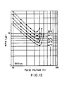
- the ferroelectric liquid crystal has a chiral smectic C phase at the operating temperature, exhibits minima in its ⁇ - V characteristics, and has a low spontaneous polarisation (preferably less than 20nC/cm 2 ).
- the cone angle at the operating temperature is between 10° and 45° and preferably 22.5°.
- the alignment layers 10, 12 are parallel - aligned and give a low surface tilt angle, for instance less than 6°, to achieve the C2 uniform alignment state.
- the uniaxial dielectric anisotropy is negative or zero.
- An example of a suitable material has a phase sequence temperature of: Sm C - 65° - Sm A - 86° - N - 98° - Iso
- N is the nematic state
- Iso is the isotropic phase.
- a memory angle of 26° is obtained at 8 volts, 29° at 9 volts and 31° at 10 volts.
- the material has ⁇ - V characteristics (without bias) at various temperatures as shown in Figure 13.
- intersections between the data electrodes 1 and the strobe electrodes 5 define individual pixels which are addressable independently of each other.
- FIG. 2 illustrates diagrammatically the relative timing of the data and strobe signals in the display shown in Figure 1.
- N strobe signals are supplied in sequence to groups of N strobe electrodes, where N is an integer greater than one.
- the N strobe signals are supplied simultaneously to the N strobe electrodes of each group.
- N is equal to two.
- strobe signals Vs1 and Vs2 are supplied simultaneously to the corresponding strobe electrodes in a first line address time (LAT) from t 0 to t 1
- strobe signals Vs3 and Vs4 are supplied simultaneously to their respective strobe electrodes in a succeeding LAT from t 1 to t 2 .
- LAT line address time
- the data signals Vd1 to Vd4 are supplied simultaneously with each other and in synchronism with the strobe signals.
- each data signal is represented by a rectangular box in Figure 2. Also, gaps are shown between consecutive data signals for the purpose of clarity although, in practice, consecutive data signals are contiguous.
- the strobe and data signals are inverted in polarity in alternate frames.
- Blanking pulses for resetting to black or white states all pixels belonging to the strobed electrodes may be supplied before the strobe signals.
- the blanking and strobe pulses are DC balanced so that the polarity of these pulses need not be inverted from frame to frame.
- FIG. 3 A first set of data and strobe waveforms is illustrated in Figure 3.
- each LAT such as the first LAT is subdivided into time slots, for instance as indicated at t a , t b and t c for four time slots per LAT.
- Figure 3 illustrates the two strobe waveforms referred to as Strobe-A and Strobe-B which are applied simultaneously to the pairs of strobe electrodes during each LAT.
- the data signals actually supplied to the data electrodes are selected from the four signals D-01 to D-04 illustrated in Figure 3 depending on the image data to be displayed in the two rows of pixels addressed in each LAT.
- the resultant waveforms appearing across the pixels for all of the combinations of strobe and data signals are shown in Figure 3.
- the strobe signals Strobe-A and Strobe-B are different from each other but are repeated during each LAT.
- Each strobe signal comprises a prepulse period followed by a strobe pulse.
- the prepulse periods are those periods before the amplitude of the strobe signal reaches 50% of its maximum value.
- the prepulse periods of the different strobe signals are different. As shown in Figure 3, the prepulse period of the strobe signal Strobe-A comprises the first two time slots whereas the prepulse period of the strobe signal Strobe-B comprises the first time slot.
- each data signal has no net DC component.
- the data signals have the same RMS voltage.
- the data signals have the same polarity behaviour with time.
- each data signal comprises a positive pulse followed by a negative pulse.
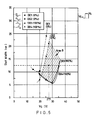
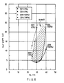
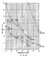
- Figures 4 and 5 illustrate the ⁇ -V characteristics of the pixels for the strobe signals Strobe-A and Strobe-B, respectively, with the different data signals.
- the strobe signals occupy four time slots of 12.5 microseconds to give an LAT of 50 microseconds.
- Strobe-A has an amplitude of 25 volts whereas Strobe-B has an amplitude of 27.5 volts.
- Each of the data signals comprises a positive pulse and a negative pulse, each of which has an amplitude Va, for instance, of 8 volts giving an RMS value of 5.66 volts for all of the data signals.
- N strobe electrodes are strobed at a time
- all of the pixels of the N rows can be independently addressed.
- the optical state of a pixel is unswitched when the waveform across it is such that the average value in the first two time slots is negative.
- the optical state of a pixel is switched when the waveform across it is such that the average value in the first two time slots is zero or positive, unless the value in the first slot is negative and the value in the second slot is greater than or equal to the value of the strobe pulse, in which case the optical state of the pixel is unswitched.
- the data signal D-01 causes switching of each pixel strobed by Strobe-A whereas each pixel strobed by Strobe-B is unswitched.
- the data signal D-02 When the data signal D-02 is supplied, no pixels are switched irrespective of which strobe signal is applied.
- the data signal D-03 When the data signal D-03 is applied, pixels strobed by Strobe-A are unswitched but pixels strobed by Strobe-B are switched.
- the data signal D-04 is applied, all pixels are switched irrespective of which strobe signal they receive.
- the full 2 N states of the two pixels in each column can be independently addressed and controlled. In the present case, there are four such states as described hereinbefore.
- the ⁇ -V curves illustrated in Figures 4 and 5 for the data signals are further classified as 0% curves which show slot widths for pixels to start switching and 100% curves which show slot width for pixels to switch fully.
- driving conditions above the 100% curves give pixel switching whereas drive conditions bellow the 0% curves give pixel non-switching.
- the area A shown in Figure 4, which is above the curves for the data signals D-01 and D-04 and below the curves for D-02 and D-03, is the effective working area for Strobe-A.
- the area B which is above the curves for the data signals D-03 and D-04 and below the curves for the data signals D-01 and D-02, is the effective working area for Strobe-B.
- data signals D-01 and D-04 give switching and data signals D-02 and D-03 give non-switching for Strobe-A.
- the data signals D-03 and D-04 give switching and the data signals D-01 and D-02 give non-switching for Strobe-B.
- the area of overlap between the areas A and B is the working area for this addressing scheme in that, under any conditions in the overlapping area, independent switching can be achieved for the two lines of pixels which are simultaneously strobed using the waveforms shown in Figure 3.
- FIG 6 illustrates another set of signals for addressing the FLCD of Figure 1.
- the strobe signals Strobe-A and Strobe-B are applied simultaneously to pairs of lines and are extended by one time slot beyond the LAT in accordance with the Malvern scheme, for instance as disclosed by J.R. Hughes and E.P. Raynes, Liquid Crystal 13, 597, 1993.
- the data signals D-01, D-02 and D-04 are as shown in Figure 3 but the data signal D-03 is replaced with a different data signal D-05. All of the data signals have an RMS voltage of 5.66 volts with Va being 8 volts.
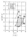
- Figures 7 and 8 show the ⁇ -V curves for Strobe-A and Strobe-B, respectively.
- the shaded areas at A and B indicate the working regions.
- pixel switching occurs for the combinations of data signals D-01 and D-04 with Strobe-A and for data signals D-05 and D-04 with Strobe-B.
- Other combinations result in non-switching of the addressed pixel.
- each pair of pixels in simultaneously strobed rows can be controlled by a common one of the data signals so as to adopt any of the four possible combinations of optical states.
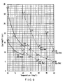
- Figures 9 and 10 illustrate the temperature dependence of driving windows using the waveforms shown in Figure 6 but with various Malvern expansions as disclosed in the Hughes and Raynes reference mentioned hereinbefore.
- Figures 9 and 10 illustrate the temperature dependence for Strobe-A and Strobe-B, respectively, and the references M1, M1.5 and M2 refer to no Malvern extension, Malvern extension by half a time slot, and Malvern extension by one time slot.
- the upper and lower curves for each expansion illustrate the maximum and minimum slot widths which give clear switching, so that driving conditions should be set between these curves.
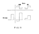
- Figure 11 illustrates the waveforms of a known driving scheme referred to as the JOERS/ALVEY driving scheme, for instance as disclosed by P.W.H. Surguy et al in Ferroelectrics, 122, 63, 1991.
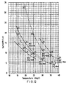
- Figure 12 corresponds to Figures 9 and 10 but illustrates the temperature dependence using the waveforms of Figure 11 with various Malvern expansions such that M1 refers to no Malvern expansion, M2 refers to Malvern expansion by one time slot, and M3 refers to Malvern expansion by two time slots.
- M1 refers to no Malvern expansion
- M2 refers to Malvern expansion by one time slot
- M3 refers to Malvern expansion by two time slots.
- the upper and lower curves for each expansion illustrate the maximum and minimum slot widths for clear switching.
- the vertical axes represent slot widths such that twice these values correspond to the LAT for a single line.
- two lines are scanned in four time slots whereas, for the known waveforms shown in Figure 11, two time slots are used to scan each line.
- the waveforms shown in Figure 6 provide a larger temperature margin and driving margin than the known waveforms shown in Figure 11.
- a device such as a ferroelectric liquid crystal device in which the effective scanning rate can be increased and/or power dissipation and heating of the device can be reduced.
- Strobe signals are supplied sequentially to groups of more than one strobe electrode of the device and any of a plurality of different data signals are supplied to each of a plurality of data electrodes of the device. It is thus possible to provide a display in which all combinations of optical states of pixels can be achieved for pixels which are connected to the same respective data electrodes and which are strobed simultaneously.
- a display panel of uniform appearance and having a rapid refresh rate is made possible.
- Such a display panel may be used, for example, as a large high content display panel.
- the frame refresh rate may be made sufficiently high such that the display panel may be used in high definition television (HDTV), even when temporal dithering techniques are applied to achieve grey scale.
Landscapes
- Engineering & Computer Science (AREA)
- Chemical & Material Sciences (AREA)
- Crystallography & Structural Chemistry (AREA)
- Physics & Mathematics (AREA)
- Computer Hardware Design (AREA)
- General Physics & Mathematics (AREA)
- Theoretical Computer Science (AREA)
- Liquid Crystal Display Device Control (AREA)
- Control Of Indicators Other Than Cathode Ray Tubes (AREA)
- Liquid Crystal (AREA)
Applications Claiming Priority (2)
| Application Number | Priority Date | Filing Date | Title |
|---|---|---|---|
| GB9712946A GB2326509A (en) | 1997-06-20 | 1997-06-20 | Addressing liquid crystal displays |
| GB9712946 | 1997-06-20 |
Publications (1)
| Publication Number | Publication Date |
|---|---|
| EP0886258A1 true EP0886258A1 (fr) | 1998-12-23 |
Family
ID=10814579
Family Applications (1)
| Application Number | Title | Priority Date | Filing Date |
|---|---|---|---|
| EP98304187A Withdrawn EP0886258A1 (fr) | 1997-06-20 | 1998-05-27 | Dispositif d'affichage à cristaux liquides ferroélectriques et méthode d'adressage d'un dispositif d'affichage à cristaux liquides ferroélectriques |
Country Status (5)
| Country | Link |
|---|---|
| US (1) | US6137463A (fr) |
| EP (1) | EP0886258A1 (fr) |
| JP (1) | JPH1172768A (fr) |
| KR (1) | KR100279684B1 (fr) |
| GB (1) | GB2326509A (fr) |
Cited By (1)
| Publication number | Priority date | Publication date | Assignee | Title |
|---|---|---|---|---|
| GB2347258A (en) * | 1999-02-24 | 2000-08-30 | Sharp Kk | Matrix array bistable devices |
Families Citing this family (1)
| Publication number | Priority date | Publication date | Assignee | Title |
|---|---|---|---|---|
| JP2006184543A (ja) | 2004-12-27 | 2006-07-13 | Sony Corp | 組レンズの組立て方法、この方法によって組立てられた組レンズ、および撮像装置 |
Citations (3)
| Publication number | Priority date | Publication date | Assignee | Title |
|---|---|---|---|---|
| JPS63151929A (ja) * | 1986-12-16 | 1988-06-24 | Matsushita Electric Ind Co Ltd | 光学変調素子の駆動方法 |
| EP0526095A2 (fr) * | 1991-07-24 | 1993-02-03 | Canon Kabushiki Kaisha | Affichage d'information |
| US5638195A (en) * | 1993-12-21 | 1997-06-10 | Canon Kabushiki Kaisha | Liquid crystal display device for improved halftone display |
Family Cites Families (12)
| Publication number | Priority date | Publication date | Assignee | Title |
|---|---|---|---|---|
| JP2612863B2 (ja) * | 1987-08-31 | 1997-05-21 | シャープ株式会社 | 表示装置の駆動方法 |
| GB8808812D0 (en) * | 1988-04-14 | 1988-05-18 | Emi Plc Thorn | Display device |
| US5289175A (en) * | 1989-04-03 | 1994-02-22 | Canon Kabushiki Kaisha | Method of and apparatus for driving ferroelectric liquid crystal display device |
| JP2592958B2 (ja) * | 1989-06-30 | 1997-03-19 | キヤノン株式会社 | 液晶装置 |
| JPH03189622A (ja) * | 1989-12-19 | 1991-08-19 | Citizen Watch Co Ltd | 強誘電性液晶素子 |
| JP3230755B2 (ja) * | 1991-11-01 | 2001-11-19 | 富士写真フイルム株式会社 | 平面型表示デバイスのマトリックス駆動方法 |
| GB9324710D0 (en) * | 1993-12-02 | 1994-01-19 | Central Research Lab Ltd | Analogue greyscale addressing |
| GB2293907A (en) * | 1994-10-03 | 1996-04-10 | Sharp Kk | Drive scheme for liquid crystal display |
| GB9407116D0 (en) * | 1994-04-11 | 1994-06-01 | Secr Defence | Ferroelectric liquid crystal display with greyscale |
| JPH0850278A (ja) * | 1994-06-01 | 1996-02-20 | Sharp Corp | 強誘電性液晶表示装置およびその階調表示駆動方法 |
| GB2293906A (en) * | 1994-10-03 | 1996-04-10 | Sharp Kk | Liquid crystal display |
| GB2294797A (en) * | 1994-11-01 | 1996-05-08 | Sharp Kk | Method of addressing a liquid crystal display |
-
1997
- 1997-06-20 GB GB9712946A patent/GB2326509A/en not_active Withdrawn
-
1998
- 1998-05-27 EP EP98304187A patent/EP0886258A1/fr not_active Withdrawn
- 1998-05-28 US US09/086,039 patent/US6137463A/en not_active Expired - Fee Related
- 1998-06-19 JP JP10173626A patent/JPH1172768A/ja not_active Withdrawn
- 1998-06-19 KR KR1019980023136A patent/KR100279684B1/ko not_active Expired - Fee Related
Patent Citations (3)
| Publication number | Priority date | Publication date | Assignee | Title |
|---|---|---|---|---|
| JPS63151929A (ja) * | 1986-12-16 | 1988-06-24 | Matsushita Electric Ind Co Ltd | 光学変調素子の駆動方法 |
| EP0526095A2 (fr) * | 1991-07-24 | 1993-02-03 | Canon Kabushiki Kaisha | Affichage d'information |
| US5638195A (en) * | 1993-12-21 | 1997-06-10 | Canon Kabushiki Kaisha | Liquid crystal display device for improved halftone display |
Non-Patent Citations (1)
| Title |
|---|
| PATENT ABSTRACTS OF JAPAN vol. 12, no. 415 (P - 781) 4 November 1988 (1988-11-04) * |
Cited By (2)
| Publication number | Priority date | Publication date | Assignee | Title |
|---|---|---|---|---|
| GB2347258A (en) * | 1999-02-24 | 2000-08-30 | Sharp Kk | Matrix array bistable devices |
| GB2347258B (en) * | 1999-02-24 | 2002-10-16 | Sharp Kk | Matrix array bistable devices |
Also Published As
| Publication number | Publication date |
|---|---|
| GB2326509A (en) | 1998-12-23 |
| KR19990007149A (ko) | 1999-01-25 |
| US6137463A (en) | 2000-10-24 |
| JPH1172768A (ja) | 1999-03-16 |
| GB9712946D0 (en) | 1997-08-20 |
| KR100279684B1 (ko) | 2001-02-01 |
Similar Documents
| Publication | Publication Date | Title |
|---|---|---|
| US5041821A (en) | Ferroelectric liquid crystal apparatus with temperature dependent DC offset voltage | |
| JP2683914B2 (ja) | 表示装置 | |
| US6075506A (en) | Display and method of operating a display | |
| KR0154356B1 (ko) | 디스플레이 장치 | |
| EP0564263B1 (fr) | Dispositif d'affichage | |
| EP0224243A2 (fr) | Dispositif de modulation optique et procédé de commande de celui-ci | |
| JPH01134346A (ja) | 強誘電性液晶表示装置及びその駆動方法並びに駆動波形発生方法 | |
| EP0691639B1 (fr) | Méthode et dispositif de commande d'un panneau d'affichage à cristaux liquides ferro-électriques | |
| JPH04269792A (ja) | マトリクス表示装置の駆動方法及びこの方法で動作し得るマトリクス表示装置 | |
| US5844537A (en) | Liquid crystal display, data signal generator, and method of addressing a liquid crystal display | |
| US6008787A (en) | Antiferrolectric liquid crystal panel and method for driving same | |
| KR100300552B1 (ko) | 광변조장치 | |
| US6351256B1 (en) | Addressing method and apparatus | |
| US6137463A (en) | Liquid crystal device and method of addressing a liquid crystal device | |
| US5764211A (en) | Apparatus and method for applying pre-pulses to row selection electrodes in a liquid crystal device to prevent patterning dependence of switching behaviour | |
| KR100324438B1 (ko) | 액정 디바이스 및 액정 디바이스의 어드레스 방법 | |
| KR100236433B1 (ko) | 강유전체 액정 장치를 어드레싱하기 위한 방법과 장치 및 강유전체 액정 장치 | |
| US6046715A (en) | Liquid crystal array device | |
| JP3093511B2 (ja) | 表示装置 | |
| JPS63249130A (ja) | 液晶装置の駆動法 | |
| GB2293905A (en) | Addressing a liquid crystal display | |
| GB2328773A (en) | Addressing a liquid crystal display | |
| JPS6134523A (ja) | 液晶装置 | |
| JPH10206825A (ja) | 液晶素子の駆動法 | |
| JPH1062754A (ja) | 液晶素子の駆動法 |
Legal Events
| Date | Code | Title | Description |
|---|---|---|---|
| PUAI | Public reference made under article 153(3) epc to a published international application that has entered the european phase |
Free format text: ORIGINAL CODE: 0009012 |
|
| AK | Designated contracting states |
Kind code of ref document: A1 Designated state(s): AT BE CH CY DE DK ES FI FR GB GR IE IT LI LU MC NL PT SE |
|
| AX | Request for extension of the european patent |
Free format text: AL;LT;LV;MK;RO;SI |
|
| AKX | Designation fees paid | ||
| STAA | Information on the status of an ep patent application or granted ep patent |
Free format text: STATUS: THE APPLICATION IS DEEMED TO BE WITHDRAWN |
|
| 18D | Application deemed to be withdrawn |
Effective date: 19990624 |
|
| REG | Reference to a national code |
Ref country code: DE Ref legal event code: 8566 |