EP0886295B1 - Panneau avant pour afficheur à plasma - Google Patents
Panneau avant pour afficheur à plasma Download PDFInfo
- Publication number
- EP0886295B1 EP0886295B1 EP98304818A EP98304818A EP0886295B1 EP 0886295 B1 EP0886295 B1 EP 0886295B1 EP 98304818 A EP98304818 A EP 98304818A EP 98304818 A EP98304818 A EP 98304818A EP 0886295 B1 EP0886295 B1 EP 0886295B1
- Authority
- EP
- European Patent Office
- Prior art keywords
- electroconductive
- film
- transparent
- layer
- front panel
- Prior art date
- Legal status (The legal status is an assumption and is not a legal conclusion. Google has not performed a legal analysis and makes no representation as to the accuracy of the status listed.)
- Expired - Lifetime
Links
Images
Classifications
-
- H—ELECTRICITY
- H05—ELECTRIC TECHNIQUES NOT OTHERWISE PROVIDED FOR
- H05K—PRINTED CIRCUITS; CASINGS OR CONSTRUCTIONAL DETAILS OF ELECTRIC APPARATUS; MANUFACTURE OF ASSEMBLAGES OF ELECTRICAL COMPONENTS
- H05K9/00—Screening of apparatus or components against electric or magnetic fields
- H05K9/0073—Shielding materials
- H05K9/0094—Shielding materials being light-transmitting, e.g. transparent, translucent
- H05K9/0096—Shielding materials being light-transmitting, e.g. transparent, translucent for television displays, e.g. plasma display panel
-
- H—ELECTRICITY
- H01—ELECTRIC ELEMENTS
- H01J—ELECTRIC DISCHARGE TUBES OR DISCHARGE LAMPS
- H01J11/00—Gas-filled discharge tubes with alternating current induction of the discharge, e.g. alternating current plasma display panels [AC-PDP]; Gas-filled discharge tubes without any main electrode inside the vessel; Gas-filled discharge tubes with at least one main electrode outside the vessel
- H01J11/10—AC-PDPs with at least one main electrode being out of contact with the plasma
-
- H—ELECTRICITY
- H01—ELECTRIC ELEMENTS
- H01J—ELECTRIC DISCHARGE TUBES OR DISCHARGE LAMPS
- H01J11/00—Gas-filled discharge tubes with alternating current induction of the discharge, e.g. alternating current plasma display panels [AC-PDP]; Gas-filled discharge tubes without any main electrode inside the vessel; Gas-filled discharge tubes with at least one main electrode outside the vessel
- H01J11/20—Constructional details
- H01J11/34—Vessels, containers or parts thereof, e.g. substrates
- H01J11/44—Optical arrangements or shielding arrangements, e.g. filters, black matrices, light reflecting means or electromagnetic shielding means
-
- H—ELECTRICITY
- H01—ELECTRIC ELEMENTS
- H01J—ELECTRIC DISCHARGE TUBES OR DISCHARGE LAMPS
- H01J2211/00—Plasma display panels with alternate current induction of the discharge, e.g. AC-PDPs
- H01J2211/20—Constructional details
- H01J2211/34—Vessels, containers or parts thereof, e.g. substrates
- H01J2211/44—Optical arrangements or shielding arrangements, e.g. filters or lenses
- H01J2211/446—Electromagnetic shielding means; Antistatic means
Definitions
- the present invention relates to a front panel for a plasma display.
- a plasma display has been drawing special interest as a display which has large surface area and is flat, however, the screen thereof generates an electromagnetic wave which exerts an influence on other apparatuses and, therefore, it is necessary to shield the wave.
- Such a front panel has problems that a large scale vacuum deposition apparatus is required and the production method thereof is complicated since formation of an electroconductive layer by vacuum deposition method and the like is required for each transparent substrate.
- JP-A-07-297591 describes a transparent electromagnetic shielding film produced by a method in which an adhesive layer and a separator are successively formed on one side of a plastic film, and a transparent electroconductive thin film and a transparent layer are successively formed on the other side.
- the shielding film is said to be useful in an optical diffuser for preventing electromagnetic noise and electrostatic induction generated from a back-light of a transmission-type liquid crystal display.
- JP-A-02-271697 describes an electrostatic and electromagnetic wave shielding material comprising a transparent conductive layer provided on one surface of a transparent film base material, a transparent adhesive layer provided on the transparent conductive layer, and a transparent substrate adhered to the transparent conductive layer through the transparent adhesive layer.
- the shielding material is said to be useful for shielding static electricity or electromagnetic waves generated from a display device.
- the present inventors have intensively investigated for developing a front panel which can efficiently shield an electromagnetic wave generated from a screen of a plasma display and can be produced in a relatively simple process. As a result, it has been found that such a front panel can be obtained by placing two or more electroconductive films on a transparent substrate.
- the present invention has been accomplished on the basis of the above findings.
- the present invention provides a front panel for a plasma display comprising a transparent substrate and two or more electroconductive films, each electroconductive film comprising a transparent polymer film with a transparent electroconductive layer on at least one surface thereof, wherein each transparent electroconductive layer has a surface resistance of 10 ⁇ per unit area or less and comprises a metal layer and dielectric layers placed on both surfaces of the metal layer.
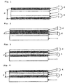
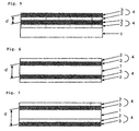
- Figs. 1 to 7 are schematic cross-sectional views of examples of the front panel for a plasma display of the present invention.
- the present invention provides a front panel for a plasma display comprising a transparent substrate and two or more electroconductive films.
- the transparent substrate in the front panel of the present invention preferably comprises a synthetic resin such as an acrylic resin, polycarbonate, polystyrene or methyl methacrylate-styrene copolymer, and the acrylic resin is especially preferred since it can be easily processed into the intended size and has excellent transparency.
- the transparent substrate used has a thickness of usually from about 0.01 mm to about 10 mm, preferably from about 0.5 mm to about 10 mm. Size of the transparent substrate is appropriately determined depending on screen size of the display.
- the transparent substrate may be substantially transparent, and further, may be colored by a dye, pigment and the like.
- Light transmittance at a wavelength in the range of from about 400 nm to about 600 nm is usually about 50% or more, preferably about 60% or more.
- the average light transmittance at a wavelength in the range of from about 850 nm to about 1000 nm is preferably about 10% or less.
- the transparent substrate having the ability to shield a near-infrared ray can be produced, for example, by molding a resin composition comprising a compound containing elemental copper, and a copolymer obtained by copolymerizing a monomer havinganunsaturated double bond and anelemental phosphorus-containing monomer (, which is described in detail, for example, in Japanese Patent Application Laid-Open (JP-A) No. Hei 6-118228), a resin composition comprising a copper compound and a phosphorus compound (, which is described in detail, for example, in Japanese Patent Application Publication (JP-B) No.
- JP-A Japanese Patent Application Laid-Open
- JP-B Japanese Patent Application Publication
- the substrate surface of at least one side on which the electroconductive film is laminated has been subjected to a hard coat treatment, so that when exposed to high temperature generated from the plasma display for long period of time, the electroconductive film is not easily released from the transparent substrate, and in the case in which the transparent substrate comprises an acrylic resin, the effect is remarkable.
- the hard coat layer used in the present invention may be a commonly used one. Examples thereof include layers prepared by polymerization and curing of polyfunctional monomers or oligomers thereof. Examples of the polyfunctional monomer include acryl-based monomers, silicon-based monomers, epoxy-based monomers and melamine-based monomers.
- a hard coat agent such as an acryl-based hard coat agent, silicon-based hard coat agent, epoxy-based hard coat agent or melamine-based hard coat agent, which contains one or more of the above polyfunctional monomers or oligomers thereof as a main component, is applied and then, is polymerized and cured to form a hard coat layer.
- acryl-based monomer for example, a polymerizable compound containing at least two (meth)acryloyloxy groups in the molecule may be listed.
- (meth)acryloyloxy represents both acryloyloxy and methacryloyloxy, and hereinafter, the term “(meth)” has an analogous meaning indicating the optional presence of a methyl substituent.
- the polymerizable compound examples include an ester compound of a polyhydric alcohol with (meth)acrylic acid, a urethane-modified (meth)acrylic oligomer obtained from a compound having an isocyanate group at the end and a (meth)acrylic acid derivative having a hydroxyl group.
- polyhydric alcohol examples include dihydric alcohol such as ethylene glycol, diethylene glycol, polyethylene glycol, propylene glycol, polypropylene glycol, propane diol, butane diol, pentane diol, hexane diol, neopentyl glycol, 2-ethyl-1,3-hexanediol, 2,2'-thiodiethanol and 1,4-cyclohexane dimethanol, and tri- or more hydric alcohol such as trimethylol propane, pentaglycerol, glycerol, pentaerythritol, diglycerol, dipentaglycerol and dipentaerythritol.
- dihydric alcohol such as ethylene glycol, diethylene glycol, polyethylene glycol, propylene glycol, polypropylene glycol, propane diol, butane diol, pentane diol, hexane diol, neopentyl glycol
- a polyvalent unsaturated carboxylic acid may be further added in small amount to prepare a mixed ester for imparting flexibility to the resulting cured film to prevent cracking.
- polyvalent unsaturated carboxylic acid examples include succinic acid, tetrahydro phthalic acid, phthalic acid, maleic acid, fumaric acid and itaconic acid.
- a urethane-modified (meth)acrylic oligomer can be obtained, for example, by reacting a (meth)acrylic acid derivative with an end isocyanate polyurethane obtained by reacting a polyisocyanate with an oligomer having a plurality of hydroxyl group.
- polyisocyanate hexamethylene diisocyanate and isophorone isocyanate may be exemplified; as the oligomer having a plurality of hydroxyl groups, polycaprolactone diol and polytetramethylene diol may be exemplified; and as the (meth)acrylic acid derivative, (meth)acrylic acid hydroxyalkylated compounds such as (meth)acrylic acid-2-hydroxyethyl and (meth)acrylic acid-2-hydroxypropyl may be exemplified.
- the polyfunctional monomer or oligomer thereof is usually, for example, mixed with an initiator and then, is applied on a transparent substrate by a common method such as a spin coating method, immersion coating method, roll-coat coating method, gravure-coat coating method and curtain flow coating method and then, it is polymerized and cured. Further, it may be diluted with various kinds of solvents before being applied, and in this case, the solvent is usually evaporated by the curing after the applying.
- a method such as an ultraviolet ray curing method, heat curing method or electron beam curing method is appropriately conducted depending on the kind of the polyfunctional monomer or oligomer thereof to be used.
- the thickness of the hard coat layer thus formed on the surface of the transparent substrate is not particularly restricted, and preferably from about 1 ⁇ m to about 20 ⁇ m. When the thickness is less than about 1 ⁇ m , interference stripes derived from the hard coat layer tend to easily occur, and when over about 20 ⁇ m, cracking tends to easily occur on the hard coat layer.
- an adhesive layer may be provided between the transparent substrate and the hard coat layer.
- the electroconductive film is obtained by placing a transparent electroconductive layer on at least one surface of a polymer film.
- the transparent electroconductive layer comprises a layer made of metal.
- Metals such as gold, silver, platinum, palladium, copper, titanium, chromium, molybdenum, nickel and zirconium may be exemplified, and these may be used alone or in combination of two or more. Among them, silver is preferred since an electroconductive film having excellent electroconductivity is easily obtained with silver.
- Dielectric layers are placed on both surfaces of the layer made of metal (which is called “a metal layer” hereinafter) since reflection of visible light by the metal layer can be lowered by the dielectric layers.
- a metal layer which is called "a metal layer” hereinafter
- Examples of the transparent electroconductive layer in view of structure include the following:
- the surface resistance of the transparent electroconductive layer is 10 ⁇ per unit area or less, preferably 6 ⁇ per unit area or less for obtaining sufficient electromagnetic wave shielding function.
- the transparent electroconductive layer can be placed on the surface of a polymer film, for example, by a method such as vacuum deposition, sputtering or ion-plating.
- the thickness of the transparent electroconductive layer is usually from about 30 nm to about 1000 nm, preferably from about 50 nm to about 500 nm. When the thickness is less than 30 nm, electroconductivity tends to be insufficient, though it depends on the kind of metal and metal oxide constituting the transparent electroconductive layer. On the other hand, when the thickness is more than 1000 nm, the transparency tends to be deficient, and for example, the tendency is remarkable when silver is used.
- the polymer film, on which the transparent electroconductive layer is formed is not particularly restricted, providing it has transparency, and in view of easy handling, processability and economy, there are usually used an ester-based resin film mainly containing an ester-based resin such as polyethylene terephthalate , an acryl-based resin film mainly containing an acryl-based resin such as polymethyl methacrylate, a cellulose-based resin film mainly containing a cellulose-based resin such as triacetylcellulose, a film mainly containing an olefin-based resin such as polypropylene or polymethylpentene, a polycarbonate-based resin film mainly containing a polycarbonate resin, or a polyvinyl chloride-based resin film mainly containing a polyvinyl chloride resin.
- the thickness of the film is usually from about 20 ⁇ m to about 500 ⁇ m.
- the electroconductive film can be obtained by cutting out of a film which is produced by using a roll film as a raw polymer film and a transparent electroconductive layer having been continuously placed on the polymer film.
- the two or more electroconductive films are placed on the transparent substrate.
- Three or more electroconductive films may be placed, however, two electroconductive films are usually placed in view of cost and procedure of the production process thereof since a desired electromagnetic-wave-shielding property is able to be obtained when two electroconductive films are placed.
- two or more electroconductive films 4 may be placed on at least one side of surface of the transparent substrate 1, or as shown in Fig. 1, the films 4 may be placed on both sides of surface of the transparent substrate 1 .
- an adhesive may be used effectively.
- the adhesive for example, an acryl-based adhesive and a rubber-based adhesive may be listed.
- the adhesive is applied on one side of surface of an electroconductive film, then, the electroconductive film is placed on a transparent substrate, then, they are press-bonded, for example using a roll press-bonding pasting machine or batch-wise pasting machine.
- the adhesive may advantageously be applied to the surface of the electroconductive film on the side opposite to the side on which the transparent electroconductive layer is placed.
- outward and inward mean “outward relative to the transparent substrate” and “inward relative to the transparent substrate” respectively.
- an electroconductive film 4 may be placed on a transparent substrate 1 so that the transparent electroconductive layer 3 faces outward, and onto this may be placed another electroconductive film 4 so that the transparent electroconductive layer 3 faces inward, or as shown in Fig. 3, an electroconductive film 4 may be placed on a transparent substrate 1 so that the transparent electroconductive layer 3 faces inward, and onto this may be placed another electroconductive film 4 so that the transparent electroconductive layer 3 also faces inward. Or as shown in Fig. 4, the electroconductive film 4 may by placed on a transparent substrate 1 so that the transparent electroconductive layer 3 faces inward, and onto this may be placed another electroconductive film 4 so that the transparent electroconductive layer 3 faces outward.
- the electroconductive film 4 may be placed on a transparent substrate 1 so that the transparent electroconductive layer 3 faces outward, and onto this may be placed another electroconductive film 4 so that the transparent electroconductive layer 3 also faces outward.
- both two transparent electroconductive layers 3 are placed internally in the structure of the front panel using an adhesive and, therefore, the front panel can not be earthed from the electroconductive layers so easily, but in the front panel shown in Fig. 4 or in Fig. 5, at least one transparent electroconductive layer is placed externally and onto that is there no adhesive, so the front panel can be easily earthed via the electroconductive layer compared with the panel shown in Fig. 2 or in Fig. 3 and, therefore, is preferred.
- one or more electroconductive films When one or more electroconductive films are placed on one side of surface of the transparent substrate, one or more electroconductive films may further be placed on the other side of surface thereof.
- the electroconductive films 4 may be placed so that both two transparent electroconductive layers 3 of the electroconductive films 4 face inward as shown in Fig. 6, however, it is preferable that at least one electroconductive film 4 is placed so that the transparent electroconductive layer 3 of the electroconductive film 4 faces inward and one electroconductive film 4 is placed so that the transparent electroconductive layer 3 of the electroconductive film 4 faces outward as shown in Fig. 7, and it is more preferable that one electroconductive film 4 is placed on each side of the transparent substrate 1 so that each transparent electroconductive layer 3 of the electroconductive films 4 faces outward as shown in Fig. 1, since the front panel shown in Fig. 7 or in Fig. 1 can be easily earthed compared with the panel shown in Fig. 6.
- the distance "d" of the transparent electroconductive layers placed on each electroconductive film is preferably 0.5 mm or more, more preferably 2 mm or more, and furthermore preferably in the range of from 2.5 mm to 10 mm in view of ability for shielding an electromagnetic wave generated from a plasma display.
- the distance "d" is essentially equal to at least the thickness of the transparent substrate, plus the thickness of the electroconductive layer, and is usually from about 0.01 mm to about 10 mm, preferably from about 0.5 mm to about 10 mm.
- the electroconductive films are placed on one side of surface of the transparent substrate, as shown in Figs. 2 to 5, especially when an electroconductive film is placed on one side of surface of the transparent substrate so that the transparent electroconductive layer faces outward, and onto this, another transparent electroconductive film is further placed on the former electroconductive film so that the transparent electroconductive layer of the latter film faces outward as shown in Fig.
- the distance "d" is essentially equal to the thickness of the polymer film consisting of the electroconductive film to be placed and is usually from about 20 ⁇ m to about 500 ⁇ m. Therefore, in view of. electromagnetic wave shielding ability, the electroconductive films are preferably placed on both sides of surface of a transparent substrate having a thickness of about 2 mm or more.
- the front panel of the present invention is obtained, and in this front panel, other films such as an anti-reflection film, near-infrared shielding film and surface protection film may be further applied on the electroconductive film.
- other films such as an anti-reflection film, near-infrared shielding film and surface protection film may be further applied on the electroconductive film.
- the anti-reflection'film is a film which is obtained by placing an anti-reflection layer on a transparent film.
- the anti-reflection film is a film having poor electroconductivity and the surface resistance thereof is usually over 50 ⁇ per unit area.
- this anti-reflection layer include a layer comprising a substance having a low refractive index, such as magnesium fluoride or silicon oxide, and a multilayer comprising a combination of a layer comprising a substance having a high refractive index such as titanium oxide, tantalum oxide, tin oxide, indium oxide, zirconium oxide or zinc oxide with a layer comprising a substance having a low refractive index.
- Aluminum oxide may be placed between the anti-reflection layer and the transparent film in the anti-reflection film.
- the anti-reflection film may have the following conformation of: a silicon oxide layer/a magnesium fluoride layer/an aluminum oxide layer/a transparent film.
- a film used as the anti-reflection film is not particularly restricted, providing it has transparency, and in view of easy handling, processability and economy, there are usually used a film mainly containing an ester-based resin such as polyethylene terephthalate, a film mainly containing an acryl-based resin such as polymethyl methacrylate, a film mainly containing a cellulose-based resin such as triacetylcellulose, a film mainly containing an olefin-based resin such as polypropylene or polymethylpentene, a film mainly containing a polycarbonate resin, or a film mainly containing a polyvinyl chloride resin.
- the thickness of the film is usually from about 20 ⁇ m to about 500 ⁇ m. It is preferable that the surface of the film has been subjected to hard coat treatment in view of hardness of the surface. The hard coat treatment is conducted in the same manner as described above.
- the anti-reflection layer can be formed on the film, for example, by a vacuum deposition method, a sputtering method and an ion-plating method, and a thickness thereof is appropriately determined depending on an effect of the anti-reflection and is usually from about 100 nm to about 500 nm.
- a stain-proofing layer may further be formed on the surface of the anti-reflection film.
- the stain-proofing layer can be easily formed, for example, by applying a solution of fluorine-based or silicon-based coupling agents on the anti-reflection film and then drying it.
- the anti-reflection film may be placed on an electroconductive film using, for example, an adhesive.
- the adhesive include an acryl-based adhesive and a rubber-based adhesive.
- the anti-reflection film may be placed on an electroconductive film in the same manner as in the electroconductive film being placed on the transparent substrate.
- a film which has been subjected to hard coat treatment, and the like may be placed on the electroconductive film as a surface protecting film.
- This surface protecting film may be placed on the electroconductive film, for example, by using an adhesive.
- an adhesive for example, an acryl-based pressure sensitive adhesive and a rubber-based pressure sensitive adhesive may be listed.
- the surface protecting film may be placed in the same manner as for the electroconductive film being placed on the transparent substrate.
- the front panel of the present invention is excellent as a front panel for a plasma display since it can effectively shield an electromagnetic wave generated from the screen of the plasma display and can be simply produced.
- Light transmittance of the front panel was measured in the range of from 400 nm to 1000 nm by using an automatic-recording spectrophotometer Model 330 manufactured by Hitachi, Ltd.
- the front panel was installed to the front face of a 20-inch plasma display and the screen was observed through the panel and then, differences in color and border of the image between before and after installing the front panel were confirmed.
- Electromagnetic wave shielding performance :
- a plasma display apparatus (Model PDS 1000, manufactured by Fujitsu General Co., Ltd.) to which the front panel has been installed was placed at a tilted angle of 15 degrees to the panel perpendicular to a domestic television, ahead of, and at a distant of 10 m from the television, and the image was exhibited.
- a remote-control signal (signal wavelength: 950 nm) was transmitted to the television from a position at an angle of 15 degrees titled in the direction opposite to the plasma display, ahead of, and at a distance of 3 m from the television to confirm that the television responds normally. Then, the plasma display apparatus was brought close to the television to measure the distance between the plasma display apparatus and the domestic television when the television became out of normal control.
- the front panel was placed in an oven at 80°C, was taken out after 1000 hours lapsed, and then the change in appearance of the front panel was visually observed.
- a transparent substrate which is acryl resin plate SUMIPEX E having size of 600 mm ⁇ 400 mm and a thickness of 4 mm, manufactured by Sumitomo Chemical Co., Ltd., and the substrate was lifted at a rate of 30 cm/minute to apply the hard coat agent on both sides of surface of the transparent substrate.
- the mixed solvent was vaporized, then, a hard coat layer was formed on both sides of surface of the transparent substrate by being irradiated by a 120 W metal halide lamp UB 0451, manufactured by AI GRAPHIC from a distance of 20 cm for 10 seconds.
- This solution was poured into a polymerization cell composed of a gasket made of polyvinyl chloride having a thickness of 3 mm and two pieces of glass plates of 620 mm ⁇ 420 mm ⁇ 10 mm, and was heated for 12 hours at 50°C and subsequently for 2 hours at 100°C for conducting thermal polymerization, to obtain a transparent substrate, which is in the form of a plate and has a size of 600 mm ⁇ 400 mm and a thickness of 3 mm, having an ability for shielding near-infrared ray.
- a urethane acrylate-based hard coat agent Koei hard M101 manufactured by Koei Chemical Industries Ltd.
- a mixed solvent comprising xylene, ethyl acetate and ethylene glycol monobutyl ether (mixing ratio 3:1:1) so that solid component content was 40%
- the substrate was lifted at a rate of 30 cm/minute to apply the hard coat agent on both sides of surface of the transparent substrate, and the mixed solvent was vaporized and then, a hard coat layer was formed on both sides of surface of the transparent substrate by being irradiated by a 120 W metal halide lamp UB 0451, manufactured by AI GRAPHIC from a distance of 20 cm for 10 seconds.
- ITO indium oxide-tin oxide
- silicon oxide layer silicon oxide layer
- ITO layer silicon oxide layer
- silicon oxide layer were sequentially placed in this order for formation of anti-reflection layers by DC magnetron sputtering method on a polyethylene terephthalate (hereinafter, referred to as PET) film having a thickness of 188 ⁇ m and being manufactured by Toyobo Co., Ltd., (trade name: ESTER FILM), to obtain an anti-reflection film.
- PET polyethylene terephthalate
- a mask film was placed on the side of surface opposite to the side of surface of the anti-reflection layer of the anti-reflection film obtained above and then, the anti-reflection film was immersed into a solution obtained above, was lifted at a rate of 15 cm/minute, to coat the both sides of surface of the film. After that, the film was left for a day at room temperature for evaporation of the mixed solvent, to form a stain-proofing layer on the anti-reflection layer.
- This front panel had a penetrating color of off-yellowish light-blue and had remarkably excellent appearance, and a reflection of a background was remarkably low. Visibility of this front panel was excellent when the front panel was installed in front of a plasma display. Further, in the remote control test, the domestic television was able to be normally controlled until the distance between the plasma display and the domestic television was shortened to 1.0 m. The evaluation results of a light transmittance, a surface reflectance, an electromagnetic wave shielding performance and a high temperature durable test are shown in Tables 1 to 4.
- This front panel had a penetrating color of off-yellowish light-blue and had excellent appearance, and a reflection of a background was remarkably low. Visibility of this front panel was excellent when the front panel was installed in front of a plasma display. Further, in the remote control test, the domestic television was able to be normally controlled until the distance between the plasma display and the domestic television was shortened to 1.3 m.
- the evaluation results of a light transmittance, a surface reflectance, an electromagnetic wave shielding performance and a high temperature durable test are shown in Tables 1 to 4.
- a front panel was obtained in the same manner as in Example 1 except that a PET film having a thickness of 50 ⁇ m manufactured by Toyobo Co., Ltd. which had been subjected to hard coat treatment was used instead of the anti-reflection film.
- This front panel was installed in front of a plasma display so that the side of surface having the electroconductive layer was used as an exhibiting screen.
- This front panel had a penetrating color of off-light-blue and had excellent appearance.
- the domestic television was able to be normally controlled until the distance between the plasma display and the domestic television was shortened to 1 0 m.
- Tables 1 to 4 The evaluation results of a light transmittance, a surface reflectance, an electromagnetic wave shielding performance and a high temperature durable test are shown in Tables 1 to 4.
- Example 3 Onto one side of surface of the same transparent substrate as used in Example 3, were placed the two electroconductive films ALTAIR XIR so that both transparent electroconductive layers of the electroconductive films faced outward as shown in Fig. 5, provided that the nearer transparent electroconductive layer to the substrate had a size of 200 mm ⁇ 200 mm and the upper transparent electroconductive layer had a size of 190 mm ⁇ 190 mm, to obtain a front panel.
- the exposed surface of the nearer transparent electroconductive layer to the substrate was seen 5 mm in each width at the periphery on the front panel, since the size of the nearer transparent electroconductive layer is larger than the other upper one.
- the placement of the electroconductive films was conducted by roll press bonding method by using an adhesive.
Landscapes
- Physics & Mathematics (AREA)
- Engineering & Computer Science (AREA)
- Plasma & Fusion (AREA)
- Microelectronics & Electronic Packaging (AREA)
- Electromagnetism (AREA)
- Shielding Devices Or Components To Electric Or Magnetic Fields (AREA)
- Devices For Indicating Variable Information By Combining Individual Elements (AREA)
- Gas-Filled Discharge Tubes (AREA)
Claims (10)
- Face avant destinée à un afficheur à plasma comprenant un substrat transparent (1) et deux ou davantage de couches électroconductrices (4), chaque couche électroconductrice (4) comprenant un film polymère transparent (2) avec une couche électroconductrice transparente (3) au moins sur une surface de celui-ci, dans laquelle chaque couche électroconductrice transparente (3) présente une résistance superficielle de 10 Ω ou moins par surface unitaire et comprend une couche métallique et des couches diélectriques placées sur les deux surfaces de la couche métallique.
- Face avant destinée à un afficheur à plasma selon la revendication 1, dans laquelle chaque couche électroconductrice transparente (3) présente une résistance superficielle de 6 Ω ou moins par surface unitaire.
- Face avant destinée à un afficheur à plasma selon la revendication 1 ou 2, dans laquelle deux ou davantage de couches électroconductrices (4) sont présentes sur un côté du substrat transparent (1).
- Face avant destinée à un afficheur à plasma selon la revendication 3, chacune desdites couches électroconductrices (4) comprenant ledit film polymère transparent (2) avec ladite couche électroconductrice transparente (3) sur une surface de celui-ci, dans laquelle une première couche électroconductrice (4) sur un côté du substrat transparent (1) est orientée de telle sorte que sa couche électroconductrice transparente (3) soit orientée vers l'extérieur par rapport au substrat transparent, et une deuxième couche électroconductrice (4) superposée à la première couche électroconductrice (4) est orientée de telle sorte que sa couche électroconductrice transparente (3) soit orientée vers l'extérieur par rapport au substrat transparent (1).
- Face avant destinée à un afficheur à plasma selon la revendication 1 ou 2, dans laquelle au moins une couche électroconductrice (4) est présente sur chaque côté du substrat transparent (1).
- Face avant destinée à un afficheur à plasma selon la revendication 5, chacune desdites couches électroconductrices (4) comprenant ledit film polymère transparent (2) avec ladite couche électroconductrice transparente (3) sur une surface de celui-ci, dans laquelle les couches électroconductrices (4) des deux côtés du substrat transparent (1) sont orientées de telle sorte que leurs couches électroconductrices soient orientées vers l'extérieur par rapport au substrat transparent.
- Face avant destinée à un afficheur à plasma selon la revendication 6, dans laquelle la distance entre la couche électroconductrice transparente (3) d'une couche électroconductrice (4) quelconque sur un côté du substrat transparent (1) et la couche électroconductrice transparente (3) d'une couche électroconductrice (4) quelconque sur le côté opposé du substrat transparent (1) est de 0,5 mm ou davantage.
- Face avant destinée à un afficheur à plasma selon l'une quelconque des revendications précédentes, qui comprend en outre, une couche dure, au moins sur une surface du substrat transparent (1) sur le côté du substrat transparent (1) sur lequel au moins une couche électroconductrice (4) est présente.
- Appareil afficheur à plasma comprenant une face avant destinée à un afficheur à plasma selon l'une quelconque des revendications précédentes.
- Procédé de blindage contre le rayonnement électromagnétique généré par un afficheur à plasma, qui comprend la mise en place, face à l'afficheur à plasma, d'une face avant destinée à un afficheur à plasma, telle que définie dans l'une quelconque des revendications 1 à 8.
Applications Claiming Priority (3)
| Application Number | Priority Date | Filing Date | Title |
|---|---|---|---|
| JP162672/97 | 1997-06-19 | ||
| JP16267297 | 1997-06-19 | ||
| JP16267297 | 1997-06-19 |
Publications (3)
| Publication Number | Publication Date |
|---|---|
| EP0886295A2 EP0886295A2 (fr) | 1998-12-23 |
| EP0886295A3 EP0886295A3 (fr) | 1999-02-10 |
| EP0886295B1 true EP0886295B1 (fr) | 2003-08-20 |
Family
ID=15759101
Family Applications (1)
| Application Number | Title | Priority Date | Filing Date |
|---|---|---|---|
| EP98304818A Expired - Lifetime EP0886295B1 (fr) | 1997-06-19 | 1998-06-18 | Panneau avant pour afficheur à plasma |
Country Status (3)
| Country | Link |
|---|---|
| US (1) | US6078139A (fr) |
| EP (1) | EP0886295B1 (fr) |
| DE (1) | DE69817263T2 (fr) |
Families Citing this family (15)
| Publication number | Priority date | Publication date | Assignee | Title |
|---|---|---|---|---|
| JP2001034177A (ja) * | 1999-07-16 | 2001-02-09 | Nitto Denko Corp | 透明電磁波シ―ルドフイルムの貼り合わせ方法 |
| KR100416083B1 (ko) * | 1999-11-02 | 2004-01-31 | 삼성에스디아이 주식회사 | 플라즈마 디스플레이 소자 |
| WO2002029830A1 (fr) * | 2000-09-29 | 2002-04-11 | Matsushita Electric Industrial Co., Ltd. | Substrat transparent a revetement anti-reflet conducteur multicouches, |
| JP2002260447A (ja) * | 2000-11-17 | 2002-09-13 | Furuya Kinzoku:Kk | 透明導電膜形成用材料とその製造方法、透明導電膜、タッチパネルとその製造方法、プラズマディスプレイとその製造方法、太陽電池とその製造方法、導電性フィルムとその製造方法、熱線反射ガラスとその製造方法、液晶表示装置とその製造方法、無機エレクトロルミネッセンス素子とその製造方法、及び、有機エレクトロルミネッセンス素子とその製造方法 |
| EP1350618B1 (fr) * | 2000-11-27 | 2009-01-14 | Teijin Limited | Film multicouche et film de reflexion proche infrarouge |
| JP2002341776A (ja) * | 2001-05-16 | 2002-11-29 | Nitto Denko Corp | ガラス割れ防止用フィルム状フィルタとプラズマ表示装置 |
| EP1280179A3 (fr) * | 2001-07-23 | 2003-09-03 | Asahi Glass Company Ltd. | Panneau d'affichage plat |
| US20050124417A1 (en) * | 2003-12-04 | 2005-06-09 | Sosnoski Michael J. | Gaming machine with electro-magnetic interference shielding |
| KR100787435B1 (ko) | 2005-11-22 | 2007-12-26 | 삼성에스디아이 주식회사 | 기체 여기 발광 소자 및 평판 표시장치 |
| WO2008099932A1 (fr) * | 2007-02-16 | 2008-08-21 | Kaneka Corporation | Film conducteur transparent et procédé de production de celui-ci |
| JP5223298B2 (ja) * | 2007-10-30 | 2013-06-26 | 横河電機株式会社 | 赤外線光源 |
| CN102137756A (zh) * | 2008-08-28 | 2011-07-27 | 三菱瓦斯化学株式会社 | 热塑性树脂层压体 |
| JP2014513845A (ja) * | 2012-04-19 | 2014-06-05 | 深▲セン▼欧菲光科技股▲フン▼有限公司 | 導電性構成要素およびその準備方法 |
| CN103631456B (zh) | 2012-08-24 | 2017-07-04 | 深圳欧菲光科技股份有限公司 | 薄膜感应器、包含该感应器的电容触摸屏及其制作方法和终端产品 |
| US9510456B2 (en) | 2012-11-09 | 2016-11-29 | Shenzhen O-Film Tech Co., Ltd. | Transparent conductor and preparation method thereof |
Family Cites Families (10)
| Publication number | Priority date | Publication date | Assignee | Title |
|---|---|---|---|---|
| US3647729A (en) * | 1967-04-10 | 1972-03-07 | Kyowa Gas Chem Ind Co Ltd | Infrared-absorbent methyl methacrylate resin composition and shaped articles thereof |
| JPS55142045A (en) * | 1979-04-20 | 1980-11-06 | Mitsubishi Rayon Co Ltd | Methacrylic resin material having excellent solar radiation absorptivity, and its preparation |
| US4732454A (en) * | 1985-04-22 | 1988-03-22 | Toray Industries, Inc. | Light-transmissible plate shielding electromagnetic waves |
| GB8713437D0 (en) * | 1987-06-09 | 1987-07-15 | Pilkington Brothers Plc | Shielding panel |
| JPH07115891B2 (ja) * | 1987-12-25 | 1995-12-13 | 旭硝子株式会社 | 建物用電磁波遮蔽窓ガラス |
| JPH02271697A (ja) * | 1989-04-13 | 1990-11-06 | Nitto Denko Corp | 静電気、電磁波シールド材 |
| GB8918859D0 (en) * | 1989-08-18 | 1989-09-27 | Pilkington Plc | Electromagnetic shielding panel |
| JP3224869B2 (ja) * | 1992-08-27 | 2001-11-05 | ダイセル化学工業株式会社 | 近赤外線吸収透明樹脂組成物及びその成形体 |
| JP3532611B2 (ja) * | 1994-04-28 | 2004-05-31 | 王子製紙株式会社 | 透明電磁波シールドフィルムおよびそれを用いた光拡散材の製造方法 |
| TW358895B (en) * | 1996-12-26 | 1999-05-21 | Sumitomo Chemical Co | Plasma display front panel |
-
1998
- 1998-06-18 US US09/099,207 patent/US6078139A/en not_active Expired - Fee Related
- 1998-06-18 DE DE69817263T patent/DE69817263T2/de not_active Expired - Fee Related
- 1998-06-18 EP EP98304818A patent/EP0886295B1/fr not_active Expired - Lifetime
Also Published As
| Publication number | Publication date |
|---|---|
| US6078139A (en) | 2000-06-20 |
| DE69817263T2 (de) | 2004-07-15 |
| EP0886295A3 (fr) | 1999-02-10 |
| EP0886295A2 (fr) | 1998-12-23 |
| DE69817263D1 (de) | 2003-09-25 |
Similar Documents
| Publication | Publication Date | Title |
|---|---|---|
| EP0886295B1 (fr) | Panneau avant pour afficheur à plasma | |
| US7521123B2 (en) | Transparent conductive laminate film, touch panel having this transparent conductive laminate film, and production method for this transparent conductive laminate film | |
| US6252703B1 (en) | Transparent laminate and filter for use for plasma display panel using the transparent laminate | |
| US9116380B2 (en) | Display panel device having touch input function | |
| US20030116270A1 (en) | Antireflection films for use with displays | |
| US6235398B1 (en) | Transparent laminate and filter for plasma display panel using the transparent laminate | |
| US6569516B1 (en) | Transparent laminate and plasma display panel filter utilizing same | |
| JP2004047456A (ja) | 透明導電材料およびタッチパネル | |
| EP0851452B1 (fr) | Panneau frontal d'afficheur à plasma | |
| EP1168004A2 (fr) | Face avant d'afficheur comprenant une couche antiréflechissante | |
| JPH1148411A (ja) | 前面板 | |
| US6111352A (en) | Explosion-proof film and cathode-ray tube | |
| KR20170097224A (ko) | 투명한 점착제층을 갖는 도전성 필름 적층체 | |
| JPH10223146A (ja) | プラズマディスプレイ用前面板 | |
| JP2000229371A (ja) | 透明積層体およびそれを用いたプラズマデイスプレイパネル用フイルタ | |
| JPH1062603A (ja) | 導電性を有する反射防止板およびこれを付与してなる光学部品 | |
| JPH10186128A (ja) | プラズマディスプレイ用前面板 | |
| JP3707263B2 (ja) | ディスプレイ用前面板 | |
| KR19980703086A (ko) | 다층 반사 방지 필름을 가진 플라스틱 광학 물품 | |
| JPH10153964A (ja) | ディスプレイ前面板 | |
| JPH1187988A (ja) | プラズマディスプレイ用前面板 | |
| JP3877356B2 (ja) | ディスプレイ用光学フィルター | |
| JP2000028813A (ja) | 光学フィルター及びその製造方法並びにプラズマディスプレイ用前面板 | |
| JP2000011902A (ja) | ディスプレイ用光学フィルター | |
| JPH11149063A (ja) | 反射防止膜付き眼鏡レンズ |
Legal Events
| Date | Code | Title | Description |
|---|---|---|---|
| PUAI | Public reference made under article 153(3) epc to a published international application that has entered the european phase |
Free format text: ORIGINAL CODE: 0009012 |
|
| AK | Designated contracting states |
Kind code of ref document: A2 Designated state(s): DE FR GB IT NL |
|
| AX | Request for extension of the european patent |
Free format text: AL;LT;LV;MK;RO;SI |
|
| PUAL | Search report despatched |
Free format text: ORIGINAL CODE: 0009013 |
|
| AK | Designated contracting states |
Kind code of ref document: A3 Designated state(s): AT BE CH CY DE DK ES FI FR GB GR IE IT LI LU MC NL PT SE |
|
| AX | Request for extension of the european patent |
Free format text: AL;LT;LV;MK;RO;SI |
|
| 17P | Request for examination filed |
Effective date: 19990722 |
|
| AKX | Designation fees paid |
Free format text: DE FR GB IT NL |
|
| 17Q | First examination report despatched |
Effective date: 20020213 |
|
| GRAH | Despatch of communication of intention to grant a patent |
Free format text: ORIGINAL CODE: EPIDOS IGRA |
|
| GRAH | Despatch of communication of intention to grant a patent |
Free format text: ORIGINAL CODE: EPIDOS IGRA |
|
| GRAA | (expected) grant |
Free format text: ORIGINAL CODE: 0009210 |
|
| AK | Designated contracting states |
Designated state(s): DE FR GB IT NL |
|
| REG | Reference to a national code |
Ref country code: GB Ref legal event code: FG4D |
|
| REF | Corresponds to: |
Ref document number: 69817263 Country of ref document: DE Date of ref document: 20030925 Kind code of ref document: P |
|
| ET | Fr: translation filed | ||
| PGFP | Annual fee paid to national office [announced via postgrant information from national office to epo] |
Ref country code: NL Payment date: 20040603 Year of fee payment: 7 |
|
| PGFP | Annual fee paid to national office [announced via postgrant information from national office to epo] |
Ref country code: FR Payment date: 20040608 Year of fee payment: 7 |
|
| PGFP | Annual fee paid to national office [announced via postgrant information from national office to epo] |
Ref country code: GB Payment date: 20040616 Year of fee payment: 7 |
|
| PLBE | No opposition filed within time limit |
Free format text: ORIGINAL CODE: 0009261 |
|
| STAA | Information on the status of an ep patent application or granted ep patent |
Free format text: STATUS: NO OPPOSITION FILED WITHIN TIME LIMIT |
|
| PGFP | Annual fee paid to national office [announced via postgrant information from national office to epo] |
Ref country code: DE Payment date: 20040701 Year of fee payment: 7 |
|
| 26N | No opposition filed |
Effective date: 20040524 |
|
| PG25 | Lapsed in a contracting state [announced via postgrant information from national office to epo] |
Ref country code: IT Free format text: LAPSE BECAUSE OF NON-PAYMENT OF DUE FEES Effective date: 20050618 Ref country code: GB Free format text: LAPSE BECAUSE OF NON-PAYMENT OF DUE FEES Effective date: 20050618 |
|
| PG25 | Lapsed in a contracting state [announced via postgrant information from national office to epo] |
Ref country code: NL Free format text: LAPSE BECAUSE OF NON-PAYMENT OF DUE FEES Effective date: 20060101 |
|
| PG25 | Lapsed in a contracting state [announced via postgrant information from national office to epo] |
Ref country code: DE Free format text: LAPSE BECAUSE OF NON-PAYMENT OF DUE FEES Effective date: 20060103 |
|
| PG25 | Lapsed in a contracting state [announced via postgrant information from national office to epo] |
Ref country code: FR Free format text: LAPSE BECAUSE OF NON-PAYMENT OF DUE FEES Effective date: 20060228 |
|
| GBPC | Gb: european patent ceased through non-payment of renewal fee |
Effective date: 20050618 |
|
| NLV4 | Nl: lapsed or anulled due to non-payment of the annual fee |
Effective date: 20060101 |
|
| REG | Reference to a national code |
Ref country code: FR Ref legal event code: ST Effective date: 20060228 |