EP0887633B1 - Montage de circuit pour détecter le passage d'une température critique d'un composant - Google Patents
Montage de circuit pour détecter le passage d'une température critique d'un composant Download PDFInfo
- Publication number
- EP0887633B1 EP0887633B1 EP98105982A EP98105982A EP0887633B1 EP 0887633 B1 EP0887633 B1 EP 0887633B1 EP 98105982 A EP98105982 A EP 98105982A EP 98105982 A EP98105982 A EP 98105982A EP 0887633 B1 EP0887633 B1 EP 0887633B1
- Authority
- EP
- European Patent Office
- Prior art keywords
- transistor
- circuit arrangement
- sense
- sense transistor
- arrangement according
- Prior art date
- Legal status (The legal status is an assumption and is not a legal conclusion. Google has not performed a legal analysis and makes no representation as to the accuracy of the status listed.)
- Expired - Lifetime
Links
Images

Classifications
-
- H—ELECTRICITY
- H03—ELECTRONIC CIRCUITRY
- H03K—PULSE TECHNIQUE
- H03K17/00—Electronic switching or gating, i.e. not by contact-making and –breaking
- H03K17/16—Modifications for eliminating interference voltages or currents
-
- G—PHYSICS
- G01—MEASURING; TESTING
- G01K—MEASURING TEMPERATURE; MEASURING QUANTITY OF HEAT; THERMALLY-SENSITIVE ELEMENTS NOT OTHERWISE PROVIDED FOR
- G01K3/00—Thermometers giving results other than momentary value of temperature
- G01K3/005—Circuits arrangements for indicating a predetermined temperature
-
- G—PHYSICS
- G01—MEASURING; TESTING
- G01K—MEASURING TEMPERATURE; MEASURING QUANTITY OF HEAT; THERMALLY-SENSITIVE ELEMENTS NOT OTHERWISE PROVIDED FOR
- G01K7/00—Measuring temperature based on the use of electric or magnetic elements directly sensitive to heat ; Power supply therefor, e.g. using thermoelectric elements
- G01K7/01—Measuring temperature based on the use of electric or magnetic elements directly sensitive to heat ; Power supply therefor, e.g. using thermoelectric elements using semiconducting elements having PN junctions
-
- H—ELECTRICITY
- H03—ELECTRONIC CIRCUITRY
- H03K—PULSE TECHNIQUE
- H03K17/00—Electronic switching or gating, i.e. not by contact-making and –breaking
- H03K17/08—Modifications for protecting switching circuit against overcurrent or overvoltage
- H03K2017/0806—Modifications for protecting switching circuit against overcurrent or overvoltage against excessive temperature
-
- Y—GENERAL TAGGING OF NEW TECHNOLOGICAL DEVELOPMENTS; GENERAL TAGGING OF CROSS-SECTIONAL TECHNOLOGIES SPANNING OVER SEVERAL SECTIONS OF THE IPC; TECHNICAL SUBJECTS COVERED BY FORMER USPC CROSS-REFERENCE ART COLLECTIONS [XRACs] AND DIGESTS
- Y10—TECHNICAL SUBJECTS COVERED BY FORMER USPC
- Y10S—TECHNICAL SUBJECTS COVERED BY FORMER USPC CROSS-REFERENCE ART COLLECTIONS [XRACs] AND DIGESTS
- Y10S323/00—Electricity: power supply or regulation systems
- Y10S323/907—Temperature compensation of semiconductor
Definitions
- Circuit arrangement for detecting the exceeding of a critical temperature of a component.
- the invention relates to a circuit arrangement for detecting the exceeding of a critical temperature of a component using at least one sense transistor having a temperature-dependent current-voltage characteristic and which is thermally connected to the device, and having a sense transistor in series switched current source.
- Such a circuit arrangement is known, for example, from EP 0 341 482 A1.
- the circuit in FIG. 1 has a bipolar transistor T 1 , to which a current source SQ is connected in series.
- the bipolar transistor T 1 is connected to the semiconductor device to be monitored for overtemperature, z.
- the current source SQ can be realized as a MOS semiconductor component, for example by an n-channel depletion transistor.
- the series connection of current source SQ and bipolar transistor T 1 is arranged between the terminals of a first and second supply potential V CC , GND.
- the base terminal of the transistor T 1 is connected to a reference voltage source VR.
- the current source SQ supplies the bipolar transistor T 1 with a constant current I B.
- a constant base voltage via the reference voltage source VR is impressed on the base terminal of the transistor T 1 .
- the bipolar transistor T 1 is blocked and its collector potential V Out corresponds to the value of the operating voltage.
- the shutdown temperature can be suitably selected.
- Such a temperature sensor arrangement must reliably detect the temperature of a semiconductor component and, in the event of an excess temperature of the semiconductor component, generate a signal which switches off the semiconductor component. Failure to do so may lead to the destruction of the semiconductor device.
- the parasitic junction leakage current is negligible at room temperature. However, at higher temperatures, usually at temperatures above 150 ° C, the parasitic leakage current reaches dangerously high levels.
- the parasitic collector substrate current I CS1 of a conventional npn bipolar transistor at 300 ° C. is already approximately 30 ⁇ A.
- Object of the present invention is therefore to provide a circuit arrangement for detecting the exceeding of its predetermined temperature of a semiconductor device, in which the mentioned parasitic leakage currents are circuitry compensated in a simple manner.
- circuit arrangement according to the invention is that the parasitic leakage currents are completely compensated at the sense transistor and thus the full functionality of the temperature sensor is ensured throughout the temperature range of the temperature sensor.
- Another essential advantage of the present invention is the circuitally simple implementation. Although the parasitic leakage currents can be reduced in the prior art, this circuitry reduction requires considerable circuit complexity. In addition, the parasitic leakage currents can never be completely eliminated over the entire temperature range.
- the device to be examined is usually a semiconductor device.
- this is preferably a power semiconductor component, for example a DMOS transistor or an SPT transistor.
- the invention also proves advantageous for applications with other devices that are not necessarily made of semiconductor material.
- the sense transistor is formed as an npn bipolar transistor.
- the sense transistor can also be realized as a pnp bipolar transistor or by a similar semiconductor device.
- the circuit arrangement for compensation of the parasitic leakage currents is formed by a measuring transistor and by two current mirror circuit.
- the measuring transistor is advantageously arranged in the immediate vicinity of the sense transistor, so that it is exposed to the same ambient temperature.
- the measuring transistor measures the parasitic leakage currents at the sense transistor.
- the parasitic collector base leakage current and the parasitic collector substrate leakage current can be compensated via the two current mirror circuits. It is particularly advantageous if the measuring transistor of the same conductivity type and identical to the sense transistor is constructed.
- a voltage divider can be connected upstream, via which the voltage tap is taken from the reference voltage source.
- the resistor is designed as a calibratable voltage divider.
- the current source can also be realized as a switchable, field-effect-controlled semiconductor component.
- a MOSFET is usually provided here.
- the driver circuit includes a current limit that is about 2 amperes. Since short-circuit strength is required at 40 volts drain / source voltage, it becomes necessary to use the temperature sensor at the potentially hottest point of the semiconductor device, i. H. in the middle of the DMOS power transistor. The duration of the thermal wave from the hottest point of the temperature sensor would otherwise lead to the thermal destruction of the power transistor before the overtemperature detection by the temperature sensor.
- the temperature sensor for example, at a switch-on of at least 2 ms without response of the temperature sensor in the event of non-short-circuit under the condition U DS ⁇ 18 V, I D ⁇ 2 A be functional.
- the temperature at the edge of the transistor can be about 200 ° C, depending on the starting temperature , while the temperature at the transistor center after that time is about 300 ° C.
- the mentioned high temperatures are not a reliability problem since they can occur at most 100 times for a maximum of 2 ms over the entire lifetime of the integrated circuit.
- elementary in such temperature measurement is that it defines and succeeds. Such requirements are required in particular for the specification of an airbag sensor.
- FIG. 2 shows a completely compensated temperature sensor according to the invention.
- the same or functionally identical elements as in Figure 1 are provided with the same reference numerals.
- FIG. 2 shows a sense transistor T 1 which is arranged in the center of a semiconductor component HLB, for example a DMOS transistor.
- the sense transistor T 1 is thermally connected to the semiconductor device HLB.
- Emitter side of the sense transistor T 1 is connected to the terminal of a first reference potential GND.
- Collector side of the sense transistor is connected via the current source SQ to the terminal of a second reference potential V CC .
- the base terminal of the sense transistor T 1 is also connected via a reference voltage source V R to the terminal of the first reference potential GND.
- the output signal of the temperature sensor arrangement can be tapped.
- the sense transistor T 1 is an npn bipolar transistor, but it may also be formed by a pnp transistor.
- the first supply potential GND is here the potential of the reference ground.
- the current source SQ can also be realized by a switchable field-effect-controlled semiconductor component, for example by an n-channel depletion MOSFET.
- a measuring transistor T 2 is arranged.
- the base / emitter path of the measuring transistor T 2 is in this case short-circuited.
- the measuring transistor T 2 is arranged in the immediate vicinity of the sense transistor T 1 and is also thermally connected to the semiconductor device HLB.
- the measuring transistor T 2 of the same conductivity type, in the present example is an NPN bipolar transistor, and identical to the sense transistor T 1 is constructed.
- the first current mirror circuit consists of two npn bipolar transistors T 3 , T 4 .
- the first current mirror circuit can also be implemented by other transistor types, For example, MOSFETs to be realized.
- the use of bipolar transistors in the present embodiment is preferable because of their more favorable voltage ratios.
- a second current mirror circuit is arranged between the collector terminals of the sense transistor T 1 and the measuring transistor T 2 and the terminal of the second supply potential V CC .
- the second current mirror circuit is realized by two p-MOS junction transistors M 1 , M 2 .
- the transistors M 1 , M 2 of the second current mirror circuit also bipolar.
- the parasitic collector / base leakage currents I CB1 , I CB2 and the parasitic collector substrate leakage currents I CS1 , I CS2 are plotted on the sense transistor T 1 and on the measuring transistor T 2 .
- the sense transistor T 2 to determine the parasitic currents is disposed adjacent the center of the semiconductor device HLB to the sense transistor T. 1
- the two transistors T 1 , T 2 are of the same conductivity type and symmetrically arranged in such a way that they have as possible the same ambient temperature. Therefore, their leakage currents I CB1 , I CB2 and I CS1 , I CS2 are almost identical. This fact is valid even if the corresponding reverse voltages U CB and U CS are different at the two transistors, since the voltage dependence of the reverse current can be largely neglected.
- the second current mirror M 1 , M 2 reflects the leakage current I CS2 from the measuring transistor T 2 to the collector of the sense transistor T 1 .
- the collector substrate reverse current I CS1 of the sense transistor becomes T 1 compensated.
- the collector base leakage current I CB1 is rendered ineffective by the bipolar current mirror T 3 , T 4 and the primary impressed leakage current I CB2 such that the current balance of the leakage currents I CB1 - I CB2 at the base of the sense transistor T 1 is also equal to zero.
- the sense transistor T 1 is provided at the collector over the entire temperature range with the same current supply, which is impressed by the current source SQ.
- the impressed base / emitter voltage thus remains constant regardless of the temperature.
- the temperature shutdown value can be dimensioned in a targeted manner.
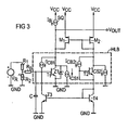
- Figure 3 shows an advantageous development of the temperature sensor arrangement according to the invention with fully compensated leakage currents corresponding to Figure 2.
- the same or functionally identical elements are provided with the same reference numerals corresponding to Figure 2.
- a Zener diode Z 1 is additionally provided for limiting the voltage between the collector / emitter terminal. Furthermore, a capacitor C is connected in parallel between the base / emitter terminal of the measuring transistor T 1 . The capacitor C renders the interference voltage originating from the supply voltage source largely harmless.
- the reference voltage source V R is a voltage divider consisting of a first resistor R 1 and a second resistor R 2 connected in parallel. At the base point between the two resistors R 1 , R 2 and the base terminal of the sense transistor T 1 , a sheet resistance R B is connected. About the voltage divider R 1 , R 2 , the reference voltage is divided down. The voltage tap then takes place via the web resistance R B.
- one of the two resistors R 1 , R 2 in the present case, the second resistor R 2 , adjustable. In this way, a defined voltage at the reference voltage source V R can be tapped.
- the response of the temperature sensor is so easily on the rotatable voltage divider R 1 , R 2 at the input, which reduces the reference voltage V R to the required value, easy to change.
Landscapes
- Physics & Mathematics (AREA)
- General Physics & Mathematics (AREA)
- Semiconductor Integrated Circuits (AREA)
- Measuring Temperature Or Quantity Of Heat (AREA)
Claims (8)
- Montage pour détecter qu'une température critique d'un composant (HLB) est dépassée, en utilisant au moins un transistor sense (T1) qui a une caractéristique courant-tension en fonction de la température et qui est relié thermiquement au composant (HLB), et comprenant une source (SQ) de courant montée en série avec le transistor sense (T1),
caractérisé
en ce qu'il est prévu un dispositif de circuit pour la compensation des courants de fuite (ICB1, ICS1) parasites sur le transistor sense (T1) et qui a les caractéristiques suivantes :- au moins un transistor (T2) de mesure, qui est relié thermiquement au composant à semi-conducteurs et qui est disposé symétriquement du transistor sense (T1), les transistors (T2) de mesure et les transistors sense (T1) étant d'une constitution identique ;- un premier circuit (T3, T4) miroir de courant, qui est monté entre les bornes de base des transistors sense (T1) et des transistors (T2) de mesure et la borne d'un premier potentiel (GND) d'alimentation ; et- un deuxième circuit (M1, M2) miroir de courant, qui est monté entre les bornes de collecteur des transistors sense (T1) et des transistors (T2) de mesure et la borne d'un deuxième potentiel (Vcc) d'alimentation. - Montage suivant la revendication 1,
caractérisé
en ce que le composant (HLB) est un composant à semi-conducteurs. - Montage suivant l'une des revendications 1 à 2,
caractérisé
en ce que le transistor sense (T1) est un transistor bipolaire. - Montage suivant l'une des revendications 1 à 3,
caractérisé
en ce qu'un diviseur (R1, R2) de tension est monté en parallèle à la section base-émetteur du transistor sense (T1). - Montage suivant la revendication 4,
caractérisé
en ce que le diviseur (R1, R2) de tension peut être étalonné. - Montage suivant l'une des revendications 1 à 5,
caractérisé
en ce qu'un condensateur (C) est monté en parallèle à la section base-émetteur du transistor sense (T1). - Montage suivant l'une des revendications 1 à 6,
caractérisé
en ce que la source (SQ) de courant est un composant à semi-conducteurs commandé par effet de champ. - Montage suivant l'une des revendications 1 à 7,
caractérisé
en ce qu'une diode (Z1) Zener est montée en parallèle à la section collecteur-émetteur du transistor sense (T1).
Applications Claiming Priority (2)
| Application Number | Priority Date | Filing Date | Title |
|---|---|---|---|
| DE19727229A DE19727229C1 (de) | 1997-06-26 | 1997-06-26 | Schaltungsanordnung zum Erfassen des Überschreitens einer kritischen Temperatur eines Bauelements |
| DE19727229 | 1997-06-26 |
Publications (2)
| Publication Number | Publication Date |
|---|---|
| EP0887633A1 EP0887633A1 (fr) | 1998-12-30 |
| EP0887633B1 true EP0887633B1 (fr) | 2006-07-26 |
Family
ID=7833760
Family Applications (1)
| Application Number | Title | Priority Date | Filing Date |
|---|---|---|---|
| EP98105982A Expired - Lifetime EP0887633B1 (fr) | 1997-06-26 | 1998-04-01 | Montage de circuit pour détecter le passage d'une température critique d'un composant |
Country Status (3)
| Country | Link |
|---|---|
| US (1) | US6144246A (fr) |
| EP (1) | EP0887633B1 (fr) |
| DE (2) | DE19727229C1 (fr) |
Families Citing this family (12)
| Publication number | Priority date | Publication date | Assignee | Title |
|---|---|---|---|---|
| US6744586B2 (en) | 2000-01-03 | 2004-06-01 | Seagate Technology Llc | Method and apparatus for monitoring temperature |
| IT1318952B1 (it) * | 2000-10-02 | 2003-09-19 | St Microelectronics Srl | Circuito di protezione alle alte correnti in convertitori perilluminazione |
| US6554470B2 (en) * | 2000-11-07 | 2003-04-29 | Maxim Integrated Products, Inc. | M-level diode junction temperature measurement method cancelling series and parallel parasitic influences |
| US6501327B1 (en) * | 2000-11-10 | 2002-12-31 | Analog Devices, Inc. | Input bias current reduction circuit for multiple input stages having a common input |
| DE10205502B4 (de) * | 2002-02-09 | 2009-01-15 | Infineon Technologies Ag | Halbleiterbauelement mit integriertem Temperatursensor |
| US6806772B2 (en) | 2002-11-06 | 2004-10-19 | Itt Manufacturing Enterprises, Inc. | Power transistor array temperature control system |
| US7000946B2 (en) * | 2003-01-21 | 2006-02-21 | Delphi Technologies, Inc. | Temperature compensated air bag control system |
| US7857509B2 (en) | 2007-08-22 | 2010-12-28 | Gm Global Technology Operations, Inc. | Temperature sensing arrangements for power electronic devices |
| JP4960808B2 (ja) * | 2007-08-30 | 2012-06-27 | セイコーインスツル株式会社 | 半導体温度センサ |
| US8057094B2 (en) * | 2007-11-16 | 2011-11-15 | Infineon Technologies Ag | Power semiconductor module with temperature measurement |
| DE102008055697B4 (de) * | 2008-06-05 | 2017-12-21 | Continental Teves Ag & Co. Ohg | Elektronische Temperaturmessschaltung |
| US9240775B2 (en) | 2013-03-12 | 2016-01-19 | Intel Deutschland Gmbh | Circuit arrangements |
Family Cites Families (10)
| Publication number | Priority date | Publication date | Assignee | Title |
|---|---|---|---|---|
| US4216394A (en) * | 1978-06-26 | 1980-08-05 | Rca Corporation | Leakage current compensation circuit |
| DE2948198C2 (de) * | 1979-11-30 | 1986-09-04 | Robert Bosch Gmbh, 7000 Stuttgart | Auswerteschaltung für elektrische Signale |
| US4503381A (en) * | 1983-03-07 | 1985-03-05 | Precision Monolithics, Inc. | Integrated circuit current mirror |
| US4613772A (en) * | 1984-04-11 | 1986-09-23 | Harris Corporation | Current compensation for logic gates |
| DE3417211A1 (de) * | 1984-05-10 | 1985-11-14 | Robert Bosch Gmbh, 7000 Stuttgart | Temperatursensor |
| JPH0693485B2 (ja) * | 1985-11-29 | 1994-11-16 | 日本電装株式会社 | 半導体装置 |
| JPH07114354B2 (ja) * | 1987-12-11 | 1995-12-06 | ローム株式会社 | トランジスタ制御回路の高温リーク補償回路 |
| DE58900553D1 (de) * | 1988-05-11 | 1992-01-23 | Siemens Ag | Schaltungsanordnung zum erfassen der uebertemperatur eines halbleiterbauelements. |
| GB9206058D0 (en) * | 1992-03-20 | 1992-05-06 | Philips Electronics Uk Ltd | A semiconductor switch and a temperature sensing circuit for such a switch |
| DE19534604C1 (de) * | 1995-09-18 | 1996-10-24 | Siemens Ag | Durch Feldeffekt steuerbares Halbleiterbauelement mit mehreren Temperatursensoren zum Schutz vor Überlastung |
-
1997
- 1997-06-26 DE DE19727229A patent/DE19727229C1/de not_active Expired - Fee Related
-
1998
- 1998-04-01 EP EP98105982A patent/EP0887633B1/fr not_active Expired - Lifetime
- 1998-04-01 DE DE59813654T patent/DE59813654D1/de not_active Expired - Lifetime
- 1998-06-26 US US09/105,230 patent/US6144246A/en not_active Expired - Lifetime
Also Published As
| Publication number | Publication date |
|---|---|
| EP0887633A1 (fr) | 1998-12-30 |
| US6144246A (en) | 2000-11-07 |
| DE19727229C1 (de) | 1998-07-23 |
| DE59813654D1 (de) | 2006-09-07 |
Similar Documents
| Publication | Publication Date | Title |
|---|---|---|
| DE69610068T2 (de) | Halbleiter-versorgungseinrichtung | |
| DE69033248T2 (de) | Schaltung zur Leistungsabgabe mit Stromerfassung | |
| DE69126826T2 (de) | Statischer Schalter | |
| DE102009061841B3 (de) | Halbleiterchip | |
| DE3500039C2 (fr) | ||
| EP0887633B1 (fr) | Montage de circuit pour détecter le passage d'une température critique d'un composant | |
| DE4133225C2 (de) | Schaltnetzteil mit Überstromschutzschaltung | |
| DE3934577A1 (de) | Stromversorgungseinrichtung mit einschaltstrombegrenzungsschaltung | |
| DE10000224B4 (de) | Leistungsverstärker mit einer Schutzschaltung | |
| DE1063713B (de) | Transistor mit temperaturkompensiertem Kollektorstrom | |
| DE69413798T2 (de) | Elektronische Leistungsvorrichtung mit drei Anschlüssen und isoliertem Gate mit einer Sättigungsausgangskennlinie veränderlicher Neigung in diskontinuierlicher Abhängigkeit vom Ausgangsstrom | |
| EP0780672A1 (fr) | Dispositif semi-conducteur contrÔlable par effet de champ, à capteur de température | |
| EP0144978A2 (fr) | Montage pour la commande d'un thyristor à l'aide d'un phototransistor | |
| EP0341482B1 (fr) | Circuit pour déterminer le suréchauffement d'un élément semi-conducteur | |
| DE4305038C2 (de) | MOSFET mit Temperaturschutz | |
| DE102006008292B4 (de) | Überlastschutz für steuerbare Stromverbraucher | |
| DE2821007A1 (de) | Impulsverstaerker | |
| DE4429903B4 (de) | Leistungshalbleiteranordnung mit Überlastschutzschaltung | |
| EP0732810B1 (fr) | Commutateur semi-conducteur commandable | |
| EP0735351B1 (fr) | Montage de circuit pour détecter la température d'un élément semi-conducteur de puissance | |
| DE4223274A1 (de) | Treiberschaltung fuer induktive lasten | |
| DE19546132C2 (de) | Schaltungsanordnung zum Schutz vor eingangsseitigem Überstrom bei Spannungszwischenkreisumrichtern | |
| EP1285483B1 (fr) | Composant semi-conducteur | |
| DE10205502B4 (de) | Halbleiterbauelement mit integriertem Temperatursensor | |
| DE19756640A1 (de) | Hilfsenergiefreier Gleichstromübertrager |
Legal Events
| Date | Code | Title | Description |
|---|---|---|---|
| PUAI | Public reference made under article 153(3) epc to a published international application that has entered the european phase |
Free format text: ORIGINAL CODE: 0009012 |
|
| AK | Designated contracting states |
Kind code of ref document: A1 Designated state(s): DE ES FR GB IE IT PT |
|
| AX | Request for extension of the european patent |
Free format text: AL;LT;LV;MK;RO;SI |
|
| 17P | Request for examination filed |
Effective date: 19990205 |
|
| AKX | Designation fees paid |
Free format text: DE ES FR GB IE IT PT |
|
| RAP1 | Party data changed (applicant data changed or rights of an application transferred) |
Owner name: INFINEON TECHNOLOGIES AG |
|
| GRAP | Despatch of communication of intention to grant a patent |
Free format text: ORIGINAL CODE: EPIDOSNIGR1 |
|
| GRAS | Grant fee paid |
Free format text: ORIGINAL CODE: EPIDOSNIGR3 |
|
| GRAA | (expected) grant |
Free format text: ORIGINAL CODE: 0009210 |
|
| AK | Designated contracting states |
Kind code of ref document: B1 Designated state(s): DE ES FR GB IE IT PT |
|
| PG25 | Lapsed in a contracting state [announced via postgrant information from national office to epo] |
Ref country code: IT Free format text: LAPSE BECAUSE OF FAILURE TO SUBMIT A TRANSLATION OF THE DESCRIPTION OR TO PAY THE FEE WITHIN THE PRESCRIBED TIME-LIMIT;WARNING: LAPSES OF ITALIAN PATENTS WITH EFFECTIVE DATE BEFORE 2007 MAY HAVE OCCURRED AT ANY TIME BEFORE 2007. THE CORRECT EFFECTIVE DATE MAY BE DIFFERENT FROM THE ONE RECORDED. Effective date: 20060726 Ref country code: IE Free format text: LAPSE BECAUSE OF FAILURE TO SUBMIT A TRANSLATION OF THE DESCRIPTION OR TO PAY THE FEE WITHIN THE PRESCRIBED TIME-LIMIT Effective date: 20060726 Ref country code: GB Free format text: LAPSE BECAUSE OF FAILURE TO SUBMIT A TRANSLATION OF THE DESCRIPTION OR TO PAY THE FEE WITHIN THE PRESCRIBED TIME-LIMIT Effective date: 20060726 |
|
| REG | Reference to a national code |
Ref country code: GB Ref legal event code: FG4D Free format text: NOT ENGLISH |
|
| REG | Reference to a national code |
Ref country code: IE Ref legal event code: FG4D Free format text: LANGUAGE OF EP DOCUMENT: GERMAN |
|
| REF | Corresponds to: |
Ref document number: 59813654 Country of ref document: DE Date of ref document: 20060907 Kind code of ref document: P |
|
| PG25 | Lapsed in a contracting state [announced via postgrant information from national office to epo] |
Ref country code: ES Free format text: LAPSE BECAUSE OF FAILURE TO SUBMIT A TRANSLATION OF THE DESCRIPTION OR TO PAY THE FEE WITHIN THE PRESCRIBED TIME-LIMIT Effective date: 20061106 |
|
| PG25 | Lapsed in a contracting state [announced via postgrant information from national office to epo] |
Ref country code: PT Free format text: LAPSE BECAUSE OF FAILURE TO SUBMIT A TRANSLATION OF THE DESCRIPTION OR TO PAY THE FEE WITHIN THE PRESCRIBED TIME-LIMIT Effective date: 20061226 |
|
| GBV | Gb: ep patent (uk) treated as always having been void in accordance with gb section 77(7)/1977 [no translation filed] |
Effective date: 20060726 |
|
| ET | Fr: translation filed | ||
| PLBE | No opposition filed within time limit |
Free format text: ORIGINAL CODE: 0009261 |
|
| STAA | Information on the status of an ep patent application or granted ep patent |
Free format text: STATUS: NO OPPOSITION FILED WITHIN TIME LIMIT |
|
| 26N | No opposition filed |
Effective date: 20070427 |
|
| PGFP | Annual fee paid to national office [announced via postgrant information from national office to epo] |
Ref country code: FR Payment date: 20070416 Year of fee payment: 10 |
|
| REG | Reference to a national code |
Ref country code: FR Ref legal event code: ST Effective date: 20081231 |
|
| PG25 | Lapsed in a contracting state [announced via postgrant information from national office to epo] |
Ref country code: FR Free format text: LAPSE BECAUSE OF NON-PAYMENT OF DUE FEES Effective date: 20080430 |
|
| PGFP | Annual fee paid to national office [announced via postgrant information from national office to epo] |
Ref country code: DE Payment date: 20170613 Year of fee payment: 20 |
|
| REG | Reference to a national code |
Ref country code: DE Ref legal event code: R071 Ref document number: 59813654 Country of ref document: DE |