EP0889447A2 - Détecteur optique pour ensembles d'examen de pièces de monnaie - Google Patents
Détecteur optique pour ensembles d'examen de pièces de monnaie Download PDFInfo
- Publication number
- EP0889447A2 EP0889447A2 EP98108480A EP98108480A EP0889447A2 EP 0889447 A2 EP0889447 A2 EP 0889447A2 EP 98108480 A EP98108480 A EP 98108480A EP 98108480 A EP98108480 A EP 98108480A EP 0889447 A2 EP0889447 A2 EP 0889447A2
- Authority
- EP
- European Patent Office
- Prior art keywords
- optical
- optical sensor
- electronic switch
- sensor according
- electronic
- Prior art date
- Legal status (The legal status is an assumption and is not a legal conclusion. Google has not performed a legal analysis and makes no representation as to the accuracy of the status listed.)
- Granted
Links
- 230000003287 optical effect Effects 0.000 title claims abstract description 42
- 230000000712 assembly Effects 0.000 title 1
- 238000000429 assembly Methods 0.000 title 1
- 230000000630 rising effect Effects 0.000 claims abstract description 6
- 239000003990 capacitor Substances 0.000 claims description 10
- 230000005540 biological transmission Effects 0.000 claims description 4
- 238000004146 energy storage Methods 0.000 abstract description 5
- 238000005265 energy consumption Methods 0.000 description 2
- 230000004888 barrier function Effects 0.000 description 1
- 238000010586 diagram Methods 0.000 description 1
- 239000004065 semiconductor Substances 0.000 description 1
- 230000001960 triggered effect Effects 0.000 description 1
- 238000010200 validation analysis Methods 0.000 description 1
Images

Classifications
-
- G—PHYSICS
- G07—CHECKING-DEVICES
- G07D—HANDLING OF COINS OR VALUABLE PAPERS, e.g. TESTING, SORTING BY DENOMINATIONS, COUNTING, DISPENSING, CHANGING OR DEPOSITING
- G07D5/00—Testing specially adapted to determine the identity or genuineness of coins, e.g. for segregating coins which are unacceptable or alien to a currency
Definitions
- the invention relates to an optical sensor in coin testing arrangements according to the preamble of claim 1.
- Coin validation arrangements several sensors are required that detect the presence report a coin, for example when entering a channel leading to the checkout e.g. B. to generate a so-called. Cashier signal.
- Accepting multiple coins Coin testers are also controlled by so-called sorting flaps by presence sensors. It is also known to fill the level in so-called coin tubes in money changers monitor with sensors. It is also known to have such presence sensors run as optical sensors. This is usually a light source and a photoelectric receiver is provided, the output signal of the photoelectric Depends on the presence of a coin in the light path.
- the optical transmitter is usually a light-emitting diode (LED) educated.
- a light-sensitive semiconductor is usually used as the optical receiver, for example a photosensitive transistor.
- the invention has for its object an optical sensor for coin testing arrangements to create that reduces energy consumption and safer against Incident light is.
- At least two are optical Transmitter operated in pulses via a corresponding electronic switch, by going to an energy storage device at intervals via an electronic switch be connected.
- the energy store is preferably a capacitor that between the control pulses for the electronic switch or the optical Transmitter generated flash pulses is charged.
- the control of the electronic Switch is made by a microprocessor, which is already in such Coin checking arrangements is provided. This also takes over the query of the optical Receiver, and expediently such that the processor the query circuit controls so that it only during the transmission pulse or during a Time when the optical transmitter emits its flash is sensitive.
- the pulsed operation of the optical transmitters saves a lot of energy, so that the sensor according to the invention, in particular in the case of battery-operated machines Coin checking arrangements is of great advantage. By removing only during the The operating time of the optical transmitters is largely eliminated.
- the optical sensor according to the invention therefore offers high operational reliability.
- optical transmitters can be connected in series, which are then the same Generate a light pulse by either one or more photosensitive receivers is received.
- optical transmitters with assigned electronic switch and energy storage arranged such that the one electronic switch with the rising and the other is operated with the falling edge of a control pulse.
- This arrangement has the advantage that only one control line for at least two optical Transmitter is required.
- Control lines of a processor tend to use them as sparingly as possible. This is achieved with the invention.
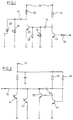
- Two photosensitive diodes 10, 12 in Fig. 1 are in series with a capacitor 14 and 16.
- the capacitors 14, 16 are connected via a resistor 18 or 20 on a common current source 22.
- a transistor 24 or 26 switched in parallel with the diodes 10, 12 in parallel with the diodes 10, 12 in parallel with a transistor 24 or 26 switched.
- a resistor 28 is connected in parallel with the diode 10 and in parallel a diode 30 connected in the opposite direction to the diode 12.
- the base of transistor 24 is through a resistor 32 to an output line of a processor (not shown) connected, which periodically emits control pulses at intervals.
- Such a control pulse is shown in Fig. 3a and designated 34.
- the duration of the pulses 34 is e.g. a few microseconds and their distance e.g. 20 to 30 microseconds.
- the pulse 34 has a rising edge 36 and a falling edge Flank 38.
- both transistors 24, 26 are blocked. Appears a Pulse 34, transistor 24 turns on, causing the previously charged capacitor 14 can discharge and generate a short current pulse in the diode 10, whereby a light pulse is emitted. With the falling edge 38 blocks Transistor 24, and capacitor 14 is recharged. The base current opens the transistor 26 and now enables the discharge of the capacitor 16, which in addition leads that the light-emitting diode 12 now emits a light pulse.
- the receiver circuit is shown. It comprises two parallel ones photosensitive transistors 40, 42.
- the operation of the circuit is like follows. In the idle state, a transistor 44 should be conductive. His collector is over one Resistor 46 connected to a current source 22. Its base is over one Resistor 48 also on this current source.
- the collector of a transistor 50 whose base is connected to the collector of transistor 44 is due to described operating mode on supply voltage.
- the collector of the transistor 50 is through a capacitor 52 with a point between the base of the transistor 44 and the resistor 48 connected. Has the voltage across capacitor 52 Supply voltage level minus the voltage drop on the base emitter path of transistor 50.
- FIG. 3b shows in FIG. 3b which pulses at the output 54 of the circuit arrangement 2 occur when the distance between the diodes 12 and 10 or 42 and 40 is not covered by a coin or the like. It's easy to see that a first pulse 56 by the rising edge 36 and a second Pulse was triggered by the falling edge 58.
- the processor can thus determine whether at the time of pulse 36, 38 (rising and falling edge), a pulse on the Receiver side is generated. Is this e.g. for the one receiving transistor 40 or 42 not the case, for example by covering the diode 10, only a pulse 58a is generated (Fig. 3c). However, if diode 12 is covered, a pulse 56b is generated (Fig. 3d).
Landscapes
- Physics & Mathematics (AREA)
- General Physics & Mathematics (AREA)
- Testing Of Coins (AREA)
- Geophysics And Detection Of Objects (AREA)
- Electronic Switches (AREA)
- Control Of Vending Devices And Auxiliary Devices For Vending Devices (AREA)
- Inspection Of Paper Currency And Valuable Securities (AREA)
Applications Claiming Priority (2)
| Application Number | Priority Date | Filing Date | Title |
|---|---|---|---|
| DE29711694U | 1997-07-03 | ||
| DE29711694U DE29711694U1 (de) | 1997-07-03 | 1997-07-03 | Optischer Sensor in Münzprüfanordnungen |
Publications (3)
| Publication Number | Publication Date |
|---|---|
| EP0889447A2 true EP0889447A2 (fr) | 1999-01-07 |
| EP0889447A3 EP0889447A3 (fr) | 1999-10-13 |
| EP0889447B1 EP0889447B1 (fr) | 2003-06-18 |
Family
ID=8042573
Family Applications (1)
| Application Number | Title | Priority Date | Filing Date |
|---|---|---|---|
| EP98108480A Expired - Lifetime EP0889447B1 (fr) | 1997-07-03 | 1998-05-09 | Détecteur optique pour ensembles d'examen de pièces de monnaie |
Country Status (3)
| Country | Link |
|---|---|
| EP (1) | EP0889447B1 (fr) |
| DE (2) | DE29711694U1 (fr) |
| ES (1) | ES2198616T3 (fr) |
Cited By (2)
| Publication number | Priority date | Publication date | Assignee | Title |
|---|---|---|---|---|
| US6314827B1 (en) | 1997-09-01 | 2001-11-13 | Kanzaki Kokyukoki Mfg. Co., Ltd. | Transmission for a working vehicle |
| BE1016016A3 (fr) * | 2003-03-14 | 2006-01-10 | Int Currency Tech | Circuit de commande d'energie a utiliser dans un distributeur automatique. |
Families Citing this family (1)
| Publication number | Priority date | Publication date | Assignee | Title |
|---|---|---|---|---|
| ES2387027B1 (es) * | 2011-02-15 | 2013-06-24 | Ojmar, S.A. | Cerradura con deteccion optica de moneda. |
Family Cites Families (4)
| Publication number | Priority date | Publication date | Assignee | Title |
|---|---|---|---|---|
| DE2055134A1 (de) * | 1970-11-10 | 1972-05-18 | Pruemm G | Elektronischer Münzprüfer |
| DE3416045A1 (de) * | 1984-04-30 | 1985-10-31 | Siemens AG, 1000 Berlin und 8000 München | Verfahren zur erkennung von muenzen bei selbstverkaeufern |
| DE4301530C1 (de) * | 1993-01-21 | 1994-06-30 | Nat Rejectors Gmbh | Induktiver Einschaltsensor für batteriebetriebene Münzprüfer |
| US5673781A (en) * | 1995-11-21 | 1997-10-07 | Coin Acceptors, Inc. | Coin detection device and associated method |
-
1997
- 1997-07-03 DE DE29711694U patent/DE29711694U1/de not_active Expired - Lifetime
-
1998
- 1998-05-09 ES ES98108480T patent/ES2198616T3/es not_active Expired - Lifetime
- 1998-05-09 DE DE59808736T patent/DE59808736D1/de not_active Expired - Lifetime
- 1998-05-09 EP EP98108480A patent/EP0889447B1/fr not_active Expired - Lifetime
Cited By (2)
| Publication number | Priority date | Publication date | Assignee | Title |
|---|---|---|---|---|
| US6314827B1 (en) | 1997-09-01 | 2001-11-13 | Kanzaki Kokyukoki Mfg. Co., Ltd. | Transmission for a working vehicle |
| BE1016016A3 (fr) * | 2003-03-14 | 2006-01-10 | Int Currency Tech | Circuit de commande d'energie a utiliser dans un distributeur automatique. |
Also Published As
| Publication number | Publication date |
|---|---|
| EP0889447A3 (fr) | 1999-10-13 |
| EP0889447B1 (fr) | 2003-06-18 |
| DE59808736D1 (de) | 2003-07-24 |
| DE29711694U1 (de) | 1997-09-18 |
| ES2198616T3 (es) | 2004-02-01 |
Similar Documents
| Publication | Publication Date | Title |
|---|---|---|
| EP1936400B1 (fr) | Lecteur laser | |
| DE3939191C2 (fr) | ||
| DE3543992A1 (de) | Feuerdetektor-einrichtung von lichtabschwaechender bauart | |
| DE2409113B2 (de) | Lichtschrankenanordnung | |
| DE3605885C2 (fr) | ||
| DE19907547A1 (de) | Optoelektronische Vorrichtung | |
| DE102018117878B4 (de) | Sicherheitslichtgitter | |
| EP0889447B1 (fr) | Détecteur optique pour ensembles d'examen de pièces de monnaie | |
| DE3518025A1 (de) | Reflexionslichtschranke | |
| EP0898368A2 (fr) | Dispositif capteur | |
| DE1947558A1 (de) | Vorrichtung zum UEberpruefen des einwandfreien Betriebes eines Laser-Entfernungsmessers | |
| DE69111579T2 (de) | Anwesenheitsnachweissystem in einem Regal einer tragbaren Einheit mit Fähigkeit zum Senden oder Empfangen eines eine Ausweiszahl enthaltenden Signals. | |
| EP0222195A1 (fr) | Procédé et dispositif pour la transmission de données au moyen de plusieurs lignes parallèles, en particulier des fibres optiques | |
| DE3611408C2 (fr) | ||
| DE3412734C2 (de) | Schaltungsanordnung zur Auswertung des normalerweise zwischen einem Minimalwert und einem Maximalwert liegenden Impedanzwertes einer eingangsseitig angeschlossenen Indikatorimpedanz | |
| DE102017119283B4 (de) | Sensorsystem | |
| EP0254125B1 (fr) | Système de signalisation de dangers | |
| DE202018104258U1 (de) | Sicherheitslichtgitter | |
| DE2600798C3 (de) | Verfahren und Schaltungsanordnung zur Funktionsprüfung von Geophonen, die in Überwachungsanlagen angeordnet sind, bzw. zur Funktionsprüfung der Überwachungsanlagen | |
| DE2337290B2 (de) | Überwachungseinrichtung für ein Thyristorventil | |
| EP4141492B1 (fr) | Agencement de barrière lumineuse et procédé de fonctionnement d'un agencement de barrière lumineuse | |
| DE3931939A1 (de) | Winkelmessvorrichtung | |
| EP0243941A2 (fr) | Procédé de détermination de la distance d'un objet et circuit pour la mise en oeuvre du procédé | |
| DE3540434A1 (de) | Schaltungsanordnung zum abfragen des zustands wenigstens einer tasteinrichtung und liefern einer anzeige durch eine anzeigeeinrichtung | |
| DE3912999A1 (de) | Recorder mit bandsensoren fuer schaltvorgaege |
Legal Events
| Date | Code | Title | Description |
|---|---|---|---|
| PUAI | Public reference made under article 153(3) epc to a published international application that has entered the european phase |
Free format text: ORIGINAL CODE: 0009012 |
|
| AK | Designated contracting states |
Kind code of ref document: A2 Designated state(s): CH DE ES FR GB IT LI NL |
|
| AX | Request for extension of the european patent |
Free format text: AL;LT;LV;MK;RO;SI |
|
| PUAL | Search report despatched |
Free format text: ORIGINAL CODE: 0009013 |
|
| AK | Designated contracting states |
Kind code of ref document: A3 Designated state(s): AT BE CH CY DE DK ES FI FR GB GR IE IT LI LU MC NL PT SE |
|
| AX | Request for extension of the european patent |
Free format text: AL;LT;LV;MK;RO;SI |
|
| RIC1 | Information provided on ipc code assigned before grant |
Free format text: 6G 07F 3/02 A, 6G 07D 5/00 B, 6G 07F 3/00 B |
|
| 17P | Request for examination filed |
Effective date: 20000321 |
|
| AKX | Designation fees paid |
Free format text: CH DE ES FR GB IT LI NL |
|
| GRAH | Despatch of communication of intention to grant a patent |
Free format text: ORIGINAL CODE: EPIDOS IGRA |
|
| RIC1 | Information provided on ipc code assigned before grant |
Free format text: 7G 07D 5/00 A, 7G 07F 5/22 B |
|
| GRAH | Despatch of communication of intention to grant a patent |
Free format text: ORIGINAL CODE: EPIDOS IGRA |
|
| GRAA | (expected) grant |
Free format text: ORIGINAL CODE: 0009210 |
|
| AK | Designated contracting states |
Designated state(s): CH DE ES FR GB IT LI NL |
|
| PG25 | Lapsed in a contracting state [announced via postgrant information from national office to epo] |
Ref country code: NL Free format text: LAPSE BECAUSE OF FAILURE TO SUBMIT A TRANSLATION OF THE DESCRIPTION OR TO PAY THE FEE WITHIN THE PRESCRIBED TIME-LIMIT Effective date: 20030618 |
|
| REG | Reference to a national code |
Ref country code: GB Ref legal event code: FG4D Free format text: NOT ENGLISH |
|
| REG | Reference to a national code |
Ref country code: CH Ref legal event code: EP |
|
| REF | Corresponds to: |
Ref document number: 59808736 Country of ref document: DE Date of ref document: 20030724 Kind code of ref document: P |
|
| GBT | Gb: translation of ep patent filed (gb section 77(6)(a)/1977) |
Effective date: 20031015 |
|
| NLV1 | Nl: lapsed or annulled due to failure to fulfill the requirements of art. 29p and 29m of the patents act | ||
| REG | Reference to a national code |
Ref country code: ES Ref legal event code: FG2A Ref document number: 2198616 Country of ref document: ES Kind code of ref document: T3 |
|
| ET | Fr: translation filed | ||
| PLBE | No opposition filed within time limit |
Free format text: ORIGINAL CODE: 0009261 |
|
| STAA | Information on the status of an ep patent application or granted ep patent |
Free format text: STATUS: NO OPPOSITION FILED WITHIN TIME LIMIT |
|
| RIC2 | Information provided on ipc code assigned after grant |
Ipc: 7G 07F 3/00 A |
|
| PG25 | Lapsed in a contracting state [announced via postgrant information from national office to epo] |
Ref country code: LI Free format text: LAPSE BECAUSE OF NON-PAYMENT OF DUE FEES Effective date: 20040531 Ref country code: CH Free format text: LAPSE BECAUSE OF NON-PAYMENT OF DUE FEES Effective date: 20040531 |
|
| 26N | No opposition filed |
Effective date: 20040319 |
|
| REG | Reference to a national code |
Ref country code: CH Ref legal event code: PL |
|
| PGFP | Annual fee paid to national office [announced via postgrant information from national office to epo] |
Ref country code: FR Payment date: 20080228 Year of fee payment: 11 |
|
| REG | Reference to a national code |
Ref country code: FR Ref legal event code: ST Effective date: 20100129 |
|
| PG25 | Lapsed in a contracting state [announced via postgrant information from national office to epo] |
Ref country code: FR Free format text: LAPSE BECAUSE OF NON-PAYMENT OF DUE FEES Effective date: 20090602 |
|
| PGFP | Annual fee paid to national office [announced via postgrant information from national office to epo] |
Ref country code: GB Payment date: 20110523 Year of fee payment: 14 |
|
| GBPC | Gb: european patent ceased through non-payment of renewal fee |
Effective date: 20120509 |
|
| PG25 | Lapsed in a contracting state [announced via postgrant information from national office to epo] |
Ref country code: GB Free format text: LAPSE BECAUSE OF NON-PAYMENT OF DUE FEES Effective date: 20120509 |
|
| PGFP | Annual fee paid to national office [announced via postgrant information from national office to epo] |
Ref country code: ES Payment date: 20140521 Year of fee payment: 17 Ref country code: IT Payment date: 20140523 Year of fee payment: 17 |
|
| PGFP | Annual fee paid to national office [announced via postgrant information from national office to epo] |
Ref country code: DE Payment date: 20140708 Year of fee payment: 17 |
|
| REG | Reference to a national code |
Ref country code: DE Ref legal event code: R119 Ref document number: 59808736 Country of ref document: DE |
|
| PG25 | Lapsed in a contracting state [announced via postgrant information from national office to epo] |
Ref country code: IT Free format text: LAPSE BECAUSE OF NON-PAYMENT OF DUE FEES Effective date: 20150509 |
|
| PG25 | Lapsed in a contracting state [announced via postgrant information from national office to epo] |
Ref country code: DE Free format text: LAPSE BECAUSE OF NON-PAYMENT OF DUE FEES Effective date: 20151201 |
|
| REG | Reference to a national code |
Ref country code: ES Ref legal event code: FD2A Effective date: 20160628 |
|
| PG25 | Lapsed in a contracting state [announced via postgrant information from national office to epo] |
Ref country code: ES Free format text: LAPSE BECAUSE OF NON-PAYMENT OF DUE FEES Effective date: 20150510 |