EP0889458A2 - Verfahren und Einrichtung zur Steuerung eines räumlichen Lichtmodulators - Google Patents
Verfahren und Einrichtung zur Steuerung eines räumlichen Lichtmodulators Download PDFInfo
- Publication number
- EP0889458A2 EP0889458A2 EP98401657A EP98401657A EP0889458A2 EP 0889458 A2 EP0889458 A2 EP 0889458A2 EP 98401657 A EP98401657 A EP 98401657A EP 98401657 A EP98401657 A EP 98401657A EP 0889458 A2 EP0889458 A2 EP 0889458A2
- Authority
- EP
- European Patent Office
- Prior art keywords
- light
- spatial light
- light modulator
- image
- pixel
- Prior art date
- Legal status (The legal status is an assumption and is not a legal conclusion. Google has not performed a legal analysis and makes no representation as to the accuracy of the status listed.)
- Withdrawn
Links
Images





Classifications
-
- G—PHYSICS
- G09—EDUCATION; CRYPTOGRAPHY; DISPLAY; ADVERTISING; SEALS
- G09G—ARRANGEMENTS OR CIRCUITS FOR CONTROL OF INDICATING DEVICES USING STATIC MEANS TO PRESENT VARIABLE INFORMATION
- G09G3/00—Control arrangements or circuits, of interest only in connection with visual indicators other than cathode-ray tubes
- G09G3/20—Control arrangements or circuits, of interest only in connection with visual indicators other than cathode-ray tubes for presentation of an assembly of a number of characters, e.g. a page, by composing the assembly by combination of individual elements arranged in a matrix no fixed position being assigned to or needed to be assigned to the individual characters or partial characters
- G09G3/34—Control arrangements or circuits, of interest only in connection with visual indicators other than cathode-ray tubes for presentation of an assembly of a number of characters, e.g. a page, by composing the assembly by combination of individual elements arranged in a matrix no fixed position being assigned to or needed to be assigned to the individual characters or partial characters by control of light from an independent source
- G09G3/36—Control arrangements or circuits, of interest only in connection with visual indicators other than cathode-ray tubes for presentation of an assembly of a number of characters, e.g. a page, by composing the assembly by combination of individual elements arranged in a matrix no fixed position being assigned to or needed to be assigned to the individual characters or partial characters by control of light from an independent source using liquid crystals
- G09G3/3611—Control of matrices with row and column drivers
- G09G3/3622—Control of matrices with row and column drivers using a passive matrix
- G09G3/3629—Control of matrices with row and column drivers using a passive matrix using liquid crystals having memory effects, e.g. ferroelectric liquid crystals
-
- G—PHYSICS
- G09—EDUCATION; CRYPTOGRAPHY; DISPLAY; ADVERTISING; SEALS
- G09G—ARRANGEMENTS OR CIRCUITS FOR CONTROL OF INDICATING DEVICES USING STATIC MEANS TO PRESENT VARIABLE INFORMATION
- G09G3/00—Control arrangements or circuits, of interest only in connection with visual indicators other than cathode-ray tubes
- G09G3/20—Control arrangements or circuits, of interest only in connection with visual indicators other than cathode-ray tubes for presentation of an assembly of a number of characters, e.g. a page, by composing the assembly by combination of individual elements arranged in a matrix no fixed position being assigned to or needed to be assigned to the individual characters or partial characters
- G09G3/34—Control arrangements or circuits, of interest only in connection with visual indicators other than cathode-ray tubes for presentation of an assembly of a number of characters, e.g. a page, by composing the assembly by combination of individual elements arranged in a matrix no fixed position being assigned to or needed to be assigned to the individual characters or partial characters by control of light from an independent source
- G09G3/3406—Control of illumination source
-
- G—PHYSICS
- G09—EDUCATION; CRYPTOGRAPHY; DISPLAY; ADVERTISING; SEALS
- G09G—ARRANGEMENTS OR CIRCUITS FOR CONTROL OF INDICATING DEVICES USING STATIC MEANS TO PRESENT VARIABLE INFORMATION
- G09G2310/00—Command of the display device
- G09G2310/02—Addressing, scanning or driving the display screen or processing steps related thereto
- G09G2310/0235—Field-sequential colour display
-
- G—PHYSICS
- G09—EDUCATION; CRYPTOGRAPHY; DISPLAY; ADVERTISING; SEALS
- G09G—ARRANGEMENTS OR CIRCUITS FOR CONTROL OF INDICATING DEVICES USING STATIC MEANS TO PRESENT VARIABLE INFORMATION
- G09G2310/00—Command of the display device
- G09G2310/02—Addressing, scanning or driving the display screen or processing steps related thereto
- G09G2310/024—Scrolling of light from the illumination source over the display in combination with the scanning of the display screen
-
- G—PHYSICS
- G09—EDUCATION; CRYPTOGRAPHY; DISPLAY; ADVERTISING; SEALS
- G09G—ARRANGEMENTS OR CIRCUITS FOR CONTROL OF INDICATING DEVICES USING STATIC MEANS TO PRESENT VARIABLE INFORMATION
- G09G2310/00—Command of the display device
- G09G2310/08—Details of timing specific for flat panels, other than clock recovery
-
- G—PHYSICS
- G09—EDUCATION; CRYPTOGRAPHY; DISPLAY; ADVERTISING; SEALS
- G09G—ARRANGEMENTS OR CIRCUITS FOR CONTROL OF INDICATING DEVICES USING STATIC MEANS TO PRESENT VARIABLE INFORMATION
- G09G2320/00—Control of display operating conditions
- G09G2320/02—Improving the quality of display appearance
- G09G2320/0233—Improving the luminance or brightness uniformity across the screen
-
- G—PHYSICS
- G09—EDUCATION; CRYPTOGRAPHY; DISPLAY; ADVERTISING; SEALS
- G09G—ARRANGEMENTS OR CIRCUITS FOR CONTROL OF INDICATING DEVICES USING STATIC MEANS TO PRESENT VARIABLE INFORMATION
- G09G2320/00—Control of display operating conditions
- G09G2320/02—Improving the quality of display appearance
- G09G2320/0247—Flicker reduction other than flicker reduction circuits used for single beam cathode-ray tubes
-
- G—PHYSICS
- G09—EDUCATION; CRYPTOGRAPHY; DISPLAY; ADVERTISING; SEALS
- G09G—ARRANGEMENTS OR CIRCUITS FOR CONTROL OF INDICATING DEVICES USING STATIC MEANS TO PRESENT VARIABLE INFORMATION
- G09G2320/00—Control of display operating conditions
- G09G2320/06—Adjustment of display parameters
- G09G2320/0626—Adjustment of display parameters for control of overall brightness
- G09G2320/064—Adjustment of display parameters for control of overall brightness by time modulation of the brightness of the illumination source
-
- G—PHYSICS
- G09—EDUCATION; CRYPTOGRAPHY; DISPLAY; ADVERTISING; SEALS
- G09G—ARRANGEMENTS OR CIRCUITS FOR CONTROL OF INDICATING DEVICES USING STATIC MEANS TO PRESENT VARIABLE INFORMATION
- G09G3/00—Control arrangements or circuits, of interest only in connection with visual indicators other than cathode-ray tubes
- G09G3/20—Control arrangements or circuits, of interest only in connection with visual indicators other than cathode-ray tubes for presentation of an assembly of a number of characters, e.g. a page, by composing the assembly by combination of individual elements arranged in a matrix no fixed position being assigned to or needed to be assigned to the individual characters or partial characters
- G09G3/2007—Display of intermediate tones
- G09G3/2018—Display of intermediate tones by time modulation using two or more time intervals
-
- G—PHYSICS
- G09—EDUCATION; CRYPTOGRAPHY; DISPLAY; ADVERTISING; SEALS
- G09G—ARRANGEMENTS OR CIRCUITS FOR CONTROL OF INDICATING DEVICES USING STATIC MEANS TO PRESENT VARIABLE INFORMATION
- G09G3/00—Control arrangements or circuits, of interest only in connection with visual indicators other than cathode-ray tubes
- G09G3/20—Control arrangements or circuits, of interest only in connection with visual indicators other than cathode-ray tubes for presentation of an assembly of a number of characters, e.g. a page, by composing the assembly by combination of individual elements arranged in a matrix no fixed position being assigned to or needed to be assigned to the individual characters or partial characters
- G09G3/2007—Display of intermediate tones
- G09G3/2018—Display of intermediate tones by time modulation using two or more time intervals
- G09G3/2022—Display of intermediate tones by time modulation using two or more time intervals using sub-frames
-
- G—PHYSICS
- G09—EDUCATION; CRYPTOGRAPHY; DISPLAY; ADVERTISING; SEALS
- G09G—ARRANGEMENTS OR CIRCUITS FOR CONTROL OF INDICATING DEVICES USING STATIC MEANS TO PRESENT VARIABLE INFORMATION
- G09G3/00—Control arrangements or circuits, of interest only in connection with visual indicators other than cathode-ray tubes
- G09G3/20—Control arrangements or circuits, of interest only in connection with visual indicators other than cathode-ray tubes for presentation of an assembly of a number of characters, e.g. a page, by composing the assembly by combination of individual elements arranged in a matrix no fixed position being assigned to or needed to be assigned to the individual characters or partial characters
- G09G3/34—Control arrangements or circuits, of interest only in connection with visual indicators other than cathode-ray tubes for presentation of an assembly of a number of characters, e.g. a page, by composing the assembly by combination of individual elements arranged in a matrix no fixed position being assigned to or needed to be assigned to the individual characters or partial characters by control of light from an independent source
Definitions
- the present invention relates to an apparatus and method for displaying an image through modulation of an incident light from a light source by a spatial light modulator which modulates the light at each pixel thereof in a binary manner.
- Liquid crystal display units using a liquid crystal panel as a spatial light modulator have widely been used as image displaying apparatuses which display an image through modulation of an incident light from a light source by the spatial light modulator which modulates the light at each pixel thereof.
- Many of such conventional image displaying apparatuses are of a type in which a TN liquid crystal or an STN liquid crystal is used as the liquid crystal panel and continuously changed in state to modulate the light intensity.
- a TN liquid crystal or an STN liquid crystal is used as the liquid crystal panel and continuously changed in state to modulate the light intensity.
- such liquid crystal panels responds slowly and cannot operate at a high speed.
- a spatial light modulator which is made of a light modulating material capable of working fast, such as ferroelectric liquid crystal (FLC).
- FLC ferroelectric liquid crystal
- the light modulating material such as the FLC is hard to continuously change in state and can normally take only two states. Therefore, the light or optical modulation by the spatial light modulator using such a light modulating material only turns on and off a light for the binary light modulation.
- a pulse width modulation is done by the spatial light modulator turning on and off the incident light.
- the human eyes have a persistence so that a quantity of incident light upon the eyes is integrated and the result of the integration is recognised as a light intensity. So, if the pulse width modulation could be effected at a sufficiently high speed, the human eyes would recognise an incident light as if the light had a gradation of intensity.
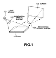
- FIG. 1 shows the concept of such an image displaying apparatus.
- a light source 101 irradiates a light through a light-irradiation optical system 102 to a spatial light modulator 103.
- the light reflected from the spatial light modulator 103 is projected by a light-projection optical system 104 onto a screen 105.
- the light source 101 is continuously turned on to provide the light at a predetermined intensity, and the light from the source 101 is modulated in pulse width by the spatial light modulator 103 which turns on and off the light source 101.
- the spatial light modulator 103 may be of a transmission type although that illustrated in FIG. 1 is of a reflection type.
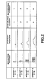
- FIG. 2 shows the basic principle of a pulse width modulation adopted in the above-mentioned image displaying apparatus to realize a display with a gradation of light intensity.
- FIG. 2 shows a relationship between patterns of modulation by the spatial light modulator 103 and light intensities recognisable by the human eyes (recognisable intensity).
- the human eyes will integrate a quantity of light reflected and modulated by the spatial light modulator 103, and recognise the integrated value as an intensity. Therefore, even if an actual light intensity is constant, as the width of a light pulse reflected from the spatial light modulator 103 is changed, the intensity recognised by the human eyes will change correspondingly to a magnitude of the pulse width change. Therefore, by controlling the pattern of modulation by the spatial light modulator 103, it is possible to effect an intensity modulation of a light.
- a characteristic (property) A in an area in the plane of the spatial light modulator 103 is different from a characteristic (property) B in another area, namely, if there exists an in-plane variation in on/off characteristic of the spatial light modulator 103, the intensity response of a light modulated by the spatial light modulator 103 will vary from one to another area with a result that an intensity recognised by the human eyes will vary. More particularly, if the spatial light modulator 103 varies in in-plane characteristic from one to another area, the light pulse intensity and shape, premises for intensity modulation through the pulse width modulation, will also vary from one to another in-plane area, so that the intensity will be non-uniform.
- This problem can be solved with a completely uniform characteristic over the plane of the spatial light modulator 103.
- it is extremely difficult to have the complete uniformity of the characteristic over the plane of the spatial light modulator 103.
- it has been difficult with the conventional image displaying apparatus to eliminate the light intensity non-uniformity due to the non-uniform in-plane distribution of the characteristic of the spatial light modulator 103.
- the minimum pulse width has to be reduced.
- the display period of one screen is about 16 msec for which a pulse width modulation should be done to realize a display with a gradation of light intensity.
- the necessary minimum pulse width has to be 62 ⁇ sec.
- the minimum pulse width has to be 15 ⁇ sec.
- the minimum pulse width should be several tens ⁇ sec. Since the TN liquid crystal and STN liquid crystal have a response speed of several msec to several hundreds msec, the minimum pulse width cannot be several tens ⁇ sec. On the contrary, the light modulating material, such as FLC, can attain a minimum pulse width of several tens ⁇ sec. However, even if a light modulating material having a high response such as FLC is used, it is necessary to use a very high voltage to excite the light modulating material in order to have such a small minimum pulse width. Namely, the requirements for excitation of the light modulating material are very difficult to meet. Therefore, a pulse width modulation in the conventional image displaying apparatus using a spatial light modulator which provides a binary modulation of a light cannot provide a satisfactory display of an image with a gradation of light intensity.
- the present invention has an object to overcome the above-mentioned drawbacks of the prior art by providing an image displaying apparatus and method which can provide a satisfactory display of an image with a gradation of light intensity even with a spatial light modulator which provides a binary light or optical modulation.
- an image displaying apparatus comprising, according to the present invention, a spatial light modulator having a plurality of pixels formed therein and modulating a light at each pixel thereof in a binary manner correspondingly to a pixel data of an image to be displayed; and a light source which is turned off during changing in state of a pixel formed in the spatial light modulator, and irradiates a light pulse to the spatial light modulator while the pixel state is steady; the light pulse from the light source being modulated by the spatial light modulator at each pixel to display the image.
- the above object can also be accomplished by providing an image displaying method comprising the following steps, according to the present invention, of: modulating a light from a light source at each pixel of a spatial light modulator which modulates a light in a binary manner correspondingly to a pixel data of an image to be displayed; turning off the light source during changing in pixel state of the spatial light modulator; and irradiating a light pulse from the light source to the spatial light modulator while the pixel state of the spatial light modulator is steady.
- the light source is turned off while the pixel state in the spatial light modulator is being changed, and the light pulse is irradiated to the spatial light modulator when the pixel of the spatial light modulator is in the steady state.
- the present invention no image is displayed while the pixel state in the spatial light modulator is being changed. Therefore, even if there exists an in-plane characteristic variation while the pixel state of the spatial light modulator is being changed, it will not cause any non-uniform intensity in an image to be displayed.
- a light pulse irradiated to the spatial light modulator is modulated to provide a gradation of light intensity. Therefore, according to the present invention, a gradation of light intensity can be attained even with the spatial light modulator which cannot respond fast.
- the light pulse may be modulated with a consideration given only to the integrated value of the light pulse quantity, not to a pulse width, number of pulses, pulse intensity, pulse shape, pulse position, etc. That is to say, the quantity of the light pulse irradiated to the spatial light modulator may be adjusted through adjustment of the pulse width, number of light pulses, pulse intensity, pulse shape, etc. based on the product of a length of irradiation time and an irradiation intensity.
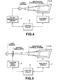
- the image displaying apparatus is destined for use as a display unit of a TV receiver, computer monitor, portable terminal, etc. As seen, it comprises a light source 1 to emit a light pulse, a pulse modulation circuit 2 to modulate the light pulse from the light source 1, a spatial light modulator 3 to modulate the light pulse from the light source 1 at each pixel thereof, a spatial light modulator drive circuit 4 to drive the spatial light modulator 3, a light-irradiation optical system 5 to irradiate the light pulse from the light source 1 to the spatial light modulator 3, a control circuit 6 to control the pulse modulation circuit 2 and spatial light modulator drive circuit 4, a screen (not illustrated in FIG. 4) onto which a light modulated by the spatial light modulator 3 is projected, and a light-projection optical system (not illustrated in FIG. 4) to project the light modulated by the spatial light modulator 3 onto the screen.
- a light source 1 to emit a light pulse
- a pulse modulation circuit 2 to modulate the light pulse from the light source 1
- control circuit 6 For displaying an image by the image displaying apparatus, data of the image is supplied to the control circuit 6.
- the control circuit 6 will control, based on the supplied image data, the pulse modulation circuit 2 and spatial light modulator drive circuit 4.
- the pulse modulation circuit 2 is controlled by the control circuit 6 to drive the light source 1 to emit a light pulse.
- the spatial light modulator drive circuit 4 is controlled by the control circuit 6 to drive the spatial light modulator 4.
- the light source 1 emits a light pulse as mentioned above. More particularly, the light pulse from the light source 1 has the width, number, etc. thereof controlled by the pulse modulation circuit 2 as will be further discussed later.
- the light source 1 may be any one of a halogen lamp, metal halide lamp, xenon lamp, light emitting diode and the like.
- a halogen lamp, metal halide lamp, xenon lamp or the like is suitable for use since it provides a sufficient quantity of light.
- a light emitting diode is suitable for use as the light source 1 since it can conveniently meet a requirement for a smaller screen and lower power consumption.
- the light source 1 should be a one which can emit red, green and blue light pulses corresponding to the three primary colours of a light and should be time-shared for display of an image with red, green and blue light pulses.
- red, green and blue light pulses corresponding to the three primary colours three independent light sources may be used for the respective colours.
- a light pulse from one light source may be divided by a dichroic mirror or the like into red, green and blue light pulses.
- the light pulse emitted from the light source 1 is irradiated to the spatial light modulator 3 through the light-irradiation optical system 5.
- the light pulse is modulated at each pixel of the spatial light modulator 3.
- This spatial light modulator 3 is made of a light modulating material capable of working fast, such as FLC, to have a plurality of pixels formed therein.
- the spatial light modulator 3 is driven by the drive circuit 4 to modulate a light at each pixel thereof in a binary manner correspondingly to a pixel data of an image to be displayed. Thereafter, the light modulated at each pixel and reflected by the spatial light modulator 3 is projected onto the screen through the light-projection optical system, so that the image is displayed on the screen.
- the spatial light modulator 3 may be of either a reflection type or a transmission type as previously mentioned.
- the spatial light modulator of the reflection type can be designed that a memory element or the like for driving the spatial light modulator at each pixel thereof is disposed at the opposite side to the light reflecting surface with the memory element not limiting the effective aperture of the pixel. Namely, in the reflection-type spatial light modulator, the effective aperture of each pixel can be increased.
- the image displaying apparatus can be designed to have a thinner structure. More particularly, the image displaying apparatus can be thinned very much by disposing a backlight at the back of the transmission-type spatial light modulator and displaying an image with a light having gone out of the backlight and passed through the spatial light modulator.
- the light source 1 is turned off during changing in state of a pixel formed in the spatial light modulator 3, and a light pulse from the light source 1 is irradiated to the spatial light modulator 3 when the state of a pixel formed in the spatial light modulator 3 is steady.
- the pulse modulation circuit 2 is connected to the light source 1 in the image displaying apparatus illustrated in FIG. 4 so that the light pulse outgoing from the light source 1 is modulated by the pulse modulation circuit 2.
- the turn-off of the light source 1 does mean that the light from the light source 1 will not reach the human eyes watching an image being displayed but not that the light source 1 has to be turned on actually.
- an optical or light modulator 7 acting as a light shutter may be disposed between the light source 1 and light-irradiation optical system 5, and a shutter drive circuit 8 to control the operation of the optical modulator 7 be provided in place of the pulse modulation circuit 2, as illustrated in FIG. 5.
- the optical modulator 7 shapes into a pulse the light emitted from the light source 1 and incident upon the spatial light modulator 3.
- the shutter drive circuit 8 By controlling the open-closing timing of the optical modulator 7 by the shutter drive circuit 8, the light pulse irradiated to the spatial light modulator 3 is controlled as to its width, number, etc.
- a mechanical shutter may be used as the optical modulator 7 but that an optical modulator using an acousto-optic modulation element (AOM) and needing no mechanism operation is suitable for the optical modulator 7.
- AOM acousto-optic modulation element
- a display period of one image to be displayed with 16 levels will be taken as one field.
- the one field is of 16 msec.
- One image having the 16 levels is comprised of at least four kinds of images different in intensity from one another. Such an image is called a "bit plane”.
- a display period of one bit plane is called a "sub-field”. That is to say, one image having 16 levels consists of at least four bit planes.
- one field consists of four sub-fields.
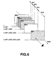
- a first bit plane BP1 is first displayed at a time point t in a period of a first sub-field SF1 as shown in FIG. 6.
- a second bit plane BP2 is displayed at a time point t + SF1 in a period of a second sub-field SF2.
- a third bit plane BP3 is displayed at a time point t + SF1 + SF2 in a period of a third sub-field SF3.
- a fourth bit plane BP4 is displayed at a time point t + SF1 + SF2 + SF3 for a period of a fourth sub-field SF4.
- the first bit plane BP1 is displayed as an image of which the intensity level recognisable by the human eyes is 1.
- the second, third and fourth bit planes. such levels are 2, 4 and 8, respectively.
- an image can be displayed with 16 levels. Namely, when these four bit planes BP1, BP2, BP3 and BP4 are displayed continuously, the human eyes will recognise an image displayed with 16 levels under the afterimage effect.
- one image having 16 levels may be composed of five or more bit planes.
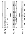
- one field is divided into four sub-fields SF1, SF2, SF3 and SF4 and bit planes BP1, BP2, BP3 and BP4 are displayed in each sub-field, as illustrated in FIG. 7A.
- these sub-fields and bit planes may be further sub-divided as illustrated in FIGS. 7B and 7C.
- the numbers of the sub-fields and of the bit planes and the arranged orders of the sub-fields and the bit planes are not limited to those in the above example illustrated in FIGS. 7A, 7B and 7C, but may be freely set.
- the fourth bit plane BP4 is further divided into bit planes BP4A and BP4B, and the fourth sub-field for which the fourth bit plane BP4 is displayed is subdivided into sub-fields SF4A and SF4B.
- the sub-fields are arranged in an order of SF4A, SF1, SF2, SF3 and SF4B, and the bit planes are displayed in an order of BP4A, BP1, BP2, BP3 and BP4B.
- the third bit plane BP3 is further divided into bit planes BP3A and BP3B, and the fourth bit plane BP4 is subdivided into bit planes BP4A and BP4B.
- the third sub-field SF3 for which the third bit plane BP3 is displayed is subdivided into sub-fields SF3A and SF3B
- the fourth sub-field for which the fourth bit plane BP4 is displayed is subdivided into sub-fields SF4A and SF4B.
- the sub-fields are arranged in an order of SF4A, SF3A, SF1, SF2, SF3B and SF4B while the bit planes are displayed in an order of BP4A, BP3A, BP1, BP2, BP3B and BP4B.
- the light source is always kept illuminated with a predetermined intensity and the spatial light modulator is driven at a high speed to adjust the intensity of each bit plane, namely, the displaying period of each bit plane.
- the spatial light modulator is driven at a high speed to adjust the intensity of each bit plane, namely, the displaying period of each bit plane.
- emitted from the light source 1 is pulsed and subjected to a pulse modulation to adjust the intensity. How the light from the light source I is pulsed and displayed as an image will be discussed in detail below.
- the light source is turned off during changing of pixel state and turned on only when the pixel state is steady.
- the spatial light modulator 3 is of a reflection type using a light modulating material having a state memorising characteristic. Namely, it suffices to apply a driving voltage when a pixel is rewritten and thereafter the pixel state is maintained even with the driving voltage made zero.
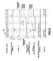
- FIG. 8 shows time changes of a light irradiated from the light source, a driving voltage applied to the spatial light modulator 3 to change the state of the pixel m, a driving voltage applied to the spatial light modulator 3 to change the state of the pixel n, a state of a portion of the spatial light modulator 3 for the pixel m, a state of a portion of the spatial light modulator 3 for the pixel n, a reflected light from the pixel m of the spatial light modulator 3, and a reflected light from the pixel n of the spatial light modulator 3.
- the light source 1 is turned off during the period (transition period) for which the pixels m and n are changed in state.
- the light source 1 is turned on only for a period (steady-state period) for which all the pixels m and n are in their steady states.
- the characteristics of all the pixels of the spatial light modulator are not uniform but the response characteristics of them vary in plane from one to another area. Therefore, if the spatial light modulator is applied with a same driving voltage to the different pixels m and n thereof, the pixels m and n may possibly respond in different manners as the case may be. Namely, even if the pixels m and n are applied with a same driving voltage, they will possibly be different in state from each other. Therefore, when an image is displayed during the transition period, an intensity non-uniformity will take place.
- the light source 1 is turned off for the transition period so that no image is displayed. Therefore, even if the pixel m responds in a different manner from the pixel n during the transition period, such a difference will not have any influence on image display. Thus, even if there takes place any in-plane characteristic variation in the spatial light modulator 3, an image free from intensity non-uniformity and having an outstanding quality can be displayed.
- the light pulse irradiated to the spatial light modulator 3 can be modulated to implement a display with many levels.
- the pulse modulation will be described below with reference to eight embodiments of the present invention.
- the aforementioned four bit planes BP1, BP2, BP3 and BP4 will be used for a display with 16 levels. That is to say, the first bit plane BP1 of which the intensity level recognisable by the human eyes is 1 is displayed for the first sub-field SF1. The second bit plane BP2 of which the intensity level recognisable by the human eyes is 2, is displayed for the second sub-field SF2. The third bit plane BP3 of which the intensity level recognisable by the human eyes is 4 is displayed for the third sub-field SF3. The fourth bit plane BP4 of which the intensity level recognisable by the human eyes is 8 is displayed for the fourth sub-field SF4.
- a display with 16 levels of intensity this number of levels being relatively small, will be described.
- the present invention can of course be applied to a display with more or less levels.
- the present invention is advantageous in that an image can be displayed with an increased number of levels even without any fast response of the spatial light modulator 3.
- eight bits of level data can be assigned to each pixel of the spatial light modulator 3 to display an image with 256 levels. Further, ten such bits can be assigned to each pixel to display an image with 1024 levels.
- bit planes of one image having 16 levels are referred to for the simplicity of description and illustration. It should also be appreciated, however, that according to the present invention, one image having 16 levels can of course be composed of five or more bit planes as seen from FIG. 7.
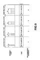
- all the sub-fields are set to have a same length of period and a light pulse from the light source is subjected to a pulse width modulation, as shown in FIG. 9.
- the light pulse is modulated with the light source 1 turned on and off by the pulse modulation circuit 2 at a predetermined timing in the image displaying apparatus as illustrated in FIG. 10. Also, in the image displaying apparatus in FIG. 6, the light pulse modulation is done with the on-off timing of the optical modulator 7 controlled by the shutter drive circuit 8. The above is also true for the second to seventh embodiments which will be described following the explanation of the first embodiment.
- a light pulse modulated to have a width corresponding to each bit plane is irradiated from the light source I to the spatial light modulator 3 for the period of each sub-field in the first embodiment.
- the light pulse irradiated to the spatial light modulator 3 is modulated to have a width ⁇ for the first sub-field SF1.
- the pulse width of the irradiated light pulse for the second sub-field SF2 is 2 ⁇ ⁇
- that of the irradiated light pulse for the third sub-field SF3 is 4 ⁇ ⁇
- that for the fourth sub-field SF4 is 8 ⁇ ⁇ .
- the level of the first bit plane BP1 recognisable by the human eyes is 1, that of the second bit plane BP2 is 2, that of the third bit plane BP3 is 4, and that of the fourth bit plane is 8.
- these bit planes BP1, BP2, BP3 and BP4 are superposed one on the other to display an image with 16 levels.
- the period of the sub-fields should be decreased to increase the number bit planes. Since the response speed of the spatial light modulator is limited, however, decreasing the sub-field period is also limited. Thus, it was difficult to increase the number of levels for use in image display in the conventional image displaying apparatus.
- the light pulse is modulated to change the level of each bit plane irrespectively of the length of period of the sub-field.
- the spatial light modulator 3 it is possible to increase the number of bit planes different in intensity level. Therefore, according to the present invention, it is possible to display an image with much more levels than ever.
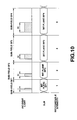
- the period of a sub-field is changed while the light pulse from the source 1 is subjected to a pulse width modulation as illustrated in FIG. 10.
- the periods of the first sub-field SF1 and second sub-field SF2 are set t1
- the periods of the third and fourth sub-fields SF3 and SF4 are set two times longer than those of the first and second sub-fields SF1 and SF2, namely, 2 x t1.
- a light pulse modulated to have a width corresponding to each bit plane is irradiated from the light source 1 to the spatial light modulator 3.
- the light pulse irradiated to the spatial light modulator 3 is modulated to have a width ⁇ .
- the second sub-field SF2 it is modulated to have a width 2 ⁇ ⁇ .
- the third sub-field SF3 it is modulated to have a field 4 ⁇ ⁇ .
- the fourth sub-field SF4 it is modulated to have a width 8 ⁇ ⁇ .
- the level of the first bit plane BP1 recognisable by the human eyes is 1, that of the second bit plane BP2 is 2, that of the third bit plane BP3 is 4, and that of the fourth bit plane BP4 is 8.
- an image is displayed with 16 levels by superposing the bit planes BP1 to BP4 one on the other.
- the length of period of the sub-field is changed to decrease the off period of the light source for a bit plane for which a light pulse having a small width is irradiated from the light source 1, thus permitting to utilise the light with a higher efficiency. Because of the reduced off period, an image flickering due to pulsation of the light from the source 1 can be suppressed.
- ratio in length of period between the sub-fields is not limited to the above example, but may be freely set.
- all the sub-fields are set to have a same length of period, the light pulse from the source 1 is subjected to a pulse width modulation, and two light pulses are emitted from the source 1 for one sub-field, as illustrated in FIG. 11.
- two light pulses modulated to have a width corresponding to bit planes within the period of each sub-field are emitted from the source 1 to the spatial light modulator 3.
- a light pulse having a width ⁇ /2 is irradiated two time points to the spatial light modulator 3 at a predetermined interval, as shown in FIG. 11.
- a light pulse having a width ⁇ is irradiated twice to the spatial light modulator 3 at the predetermined interval.
- a light pulse having a width 2 ⁇ ⁇ is irradiated twice to the spatial light modulator 3 at the predetermined interval.
- a light pulse having a width 4 ⁇ ⁇ is irradiated twice to the spatial light modulator 3 at the predetermined interval.
- the level of the first bit plane BP1 recognisable by the human eyes is 1, that of the second bit plane BP2 is 2, that of the third bit plane BP3 is 4, and that of the fourth bit plane BP4 is 8.
- an image is displayed with 16 levels by superposing the bit planes BP1 to BP4 one on the other.
- a light pulse is irradiated to the spatial light modulator 3 more than once within one sub-field period to reduce the period for which the light source 1 is continuously off, thus the sub-field period can be used effectively. Since the continuous off period is reduced, image flickering due to the pulsation of the light from the source 1 can be suppressed.
- the light pulse is emitted twice within one sub-field period.
- the light pulse may be emitted more than three times within one sub-field period if the light source 1 can be turned on and off at a sufficiently high speed.
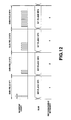
- all the sub-fields are set to have a same period to change the number of light pulses irradiated to the spatial light modulator 3 for the period of each sub-field as illustrated in FIG. 12.
- a light pulse having width T is irradiated once to the spatial light modulator 3, as illustrated in FIG. 12.
- a light pulse having width ⁇ is irradiated twice at a predetermined interval.
- a light pulse having a width ⁇ is irradiated 4 times at the predetermined interval.
- a light pulse having a width ⁇ is irradiated 8 times at the predetermined interval.
- the level of the bit plane BP 1 recognisable by the human eyes is 1. That of the bit plane BP2 is 2, that of the bit plane BP3 is 4 and that of the bit plane BP4 is 8. As having been described in the foregoing, an image is displayed with 16 levels by superposing the bit planes BP1 to BP4 one on the other.
- the sub-field period is changed while the number of light pulses irradiated to the spatial light modulator is changed for each sub-field period, as illustrated in FIG. 13.
- the periods of the first and second sub-fields SF1 and SF2 are set tl, and those of the third and fourth sub-fields SF3 and SF4 are set double that of the first and second sub-fields SF1 and SF2, namely, 2 ⁇ t1.
- the number of light pulses irradiated from the light source 1 to the spatial light modulator 3 is changed.
- a light pulse having a width ⁇ is irradiated once to the spatial light modulator 3.
- a light pulse having a width ⁇ is irradiated twice to the spatial light modulator 3 at a predetermined interval.
- a light pulse having a width ⁇ is irradiated 4 times to the spatial light modulator 3.
- a light pulse having a width ⁇ is irradiated 8 times to the spatial light modulator at the predetermined interval.
- the level of the first bit plane BP1 recognisable by the human eyes is 1, that of the second bit plane BP2 is 2, that of the third bit plane BP3 is 4, and that of the fourth bit plane BP4 is 8.
- these bit planes BP1, BP2, BP3 and BP4 are superposed one on the other to display an image with 16 levels.
- the length of the sub-field is changed to decrease the off period of the light source for a bit plane for which a small number of light pulses is irradiated from the light source 1, thus permitting to utilise the light with a higher efficiency. Because of the reduced off period, an image flickering due to pulsation of the light from the source 1 can be suppressed.
- ratio in length of period between the sub-fields is not limited to the above example, but may be freely set.
- all the sub-fields have a same length of period, the sub-field period is imaginarily divided by two, and the spatial light modulator is irradiated with different numbers of light pulses for the sub-fields, respectively, as illustrated in FIG. 14.
- the divisor of the sub-field is not limited to two but may be freely set.
- a light pulse having a width ⁇ /2 is irradiated once to the spatial light modulator 3 and for the latter half, a light pulse having a width ⁇ /2 is irradiated once to the spatial light modulator 3.
- a light pulse having a width ⁇ /2 is irradiated twice to the spatial light modulator 3 and for the latter half, a light pulse having a width T/2 is irradiated twice to the spatial light modulator 3.
- a light pulse having a width ⁇ /2 is irradiated 4 times to the spatial light modulator 3 and for the latter half, a light pulse having a width ⁇ /2 is irradiated 4 times to the spatial light modulator 3.
- a light pulse having a width ⁇ /2 is irradiated 8 times to the spatial light modulator 3 and for the latter half of the fourth sub-field SF4, a light pulse having a width ⁇ /2 is irradiated 8 times to the spatial light modulator 3.
- the level of the first bit plane BP1 recognisable by the human eyes is 1.
- the levels recognisable by the human eyes are 2, 4 and 8, respectively.
- one sub-field is divided into a plurality of sub-fields, and a predetermined number of light pulses is irradiated to each of the sub-divided sub-field, so that the period for which the light source 1 is continuously turned off can be reduced and thus the light can be used more efficiently. Because of the reduced off period, an image flicker due to pulsation of the light from the source 1 can be suppressed.
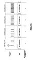
- all the sub-fields have a same length of period, and the number of light pulses irradiated to the spatial light modulator 3 is changed for each sub-field period, as illustrated in FIG. 15.
- the light pulse is emitted at time points nearly uniformly distributed over the sub-field period.
- the period of all the sub-fields is a predetermined length.
- a time point at which each pixel of the spatial light modulator 3 gets steady and a first bit plane BP1 is displayed on the spatial light modulator 3 is set Sl
- a one at which each pixel of the spatial light modulator 3 gets steady and a second bit plane BP2 is displayed on the spatial light modulator 3 is set S2
- a one at which each pixel of the spatial light modulator 3 gets steady and a third bit plane BP3 is displayed on the spatial light modulator 3 is set S3
- a one at which each pixel of the spatial light modulator 3 gets steady and a fourth bit plane BP4 is displayed on the spatial light modulator 3 is set S4.
- a light pulse having a width ⁇ /2 is irradiated twice to the spatial light modulator 3 for the first sub-field SF1.
- the light pulse is irradiated at a time point S1 + t/3, and at a time point S1 + 2 ⁇ t/3, respectively.
- a light pulse having a width ⁇ /2 is irradiated 4 times to the spatial light modulator 3.
- the light pulse is irradiated at a time point S2 + t/5, at a time point S2 + 2 ⁇ t/5, at a time point S2 + 3 ⁇ t/5, and at a time point S2 + 4 ⁇ t/5, respectively.
- a light pulse having a width ⁇ /2 is irradiated 8 times to the spatial light modulator 3.
- the light pulse is irradiated at a time point S3 + t/9, at a time point S3 + 2 ⁇ t/9, at a time point S3 + 3 ⁇ t/9, at a time point S3 + 4 ⁇ t/9, at a time point S3 + 5 ⁇ t/9, at a time point S3 + 6 ⁇ t/9, at a time point S3 + 7 ⁇ t/9, and at a time point S3 + 8 ⁇ t/9, respectively.
- a light pulse having a width ⁇ /2 is irradiated 16 times to the spatial light modulator 3.
- the light pulse is irradiated at a time point S4 + t/17, at a time point S4 + 2 ⁇ t/17, at a time point S4 + 3 ⁇ t/17, at a time point S4 + 4 ⁇ t/17, at a time point S4 + 5 ⁇ t/17, at a time point S4 + 6 ⁇ t/17, at a time point S4 + 7 ⁇ t/17, at a time point S4 + 8 ⁇ t/17, at a time point S4 + 9 ⁇ t/17, at a time point S4 + 10 ⁇ t/17, at a time point S4 + 11 ⁇ t/17, at a time point S4 + 12 ⁇ t/17, at a time point S4 + 13 ⁇ t/17, at a time point S
- the level of the first bit plane BP1 recognisable by the human eyes is 1, that of the second bit plane BP2 is 2, that of the third bit plane BP3 is 4, and that of the fourth bit plane BP4 is 8.
- an image is displayed with 16 levels by superposing the bit planes one on the other.
- a light pulse is emitted at time points nearly uniformly distributed over the entire sub-field period to reduce the period for which the light source 1 is continuously off, thus the sub-field period can be used effectively. Since the continuous off period is reduced, image flicker due to the pulsation of the light from the source 1 can be suppressed.
- the sub-field period is changed in length while the number of light pulses irradiated to the spatial light modulator 3 is changed for each of the sub-field periods, as shown in FIG. 16. Also, a light pulse is emitted at time points nearly uniformly distributed over the entire sub-field period.
- each pixel of the spatial light modulator 3 gets steady and the first bit plane BP2 is displayed on the spatial light modulator 3, both at a time point S2. Furthermore, it is assumed that the state of each pixel of the spatial light modulator 3 gets steady and the first bit plane BP3 is displayed on the spatial light modulator 3, both at a time point S3. Also it is assumed that each pixel of the spatial light modulator 3 is in the steady state and the first bit plane BP4 is displayed on the spatial light modulator 3, both at a time point S4.
- ratio in period between the sub-fields is not limited to the above but can be freely set.
- the length of the steady-state period of the spatial light modulator 3 within the periods of the first and second sub-fields SF1 and SF2 should preferably be t while that within the periods of the third and fourth sub-fields SF3 and SF4 should preferably be 2 t.
- a light pulse having a width ⁇ /2 is irradiated twice to the spatial light modulator 3 for the first sub-field SF1.
- the light pulse is irradiated at a time point S1 + t/3, and at a time point S1 + 2 ⁇ t/3, respectively.
- a light pulse having a width ⁇ /2 is irradiated 4 times to the spatial light modulator 3.
- the light pulse is irradiated at a time point S2 + t/5, at a time point S2 + 2 ⁇ t/5, at a time point S2 + 3 ⁇ t/5, and at a time point S2 + 4 ⁇ t/5, respectively.
- a light pulse having a width ⁇ /2 is irradiated 8 times to the spatial light modulator 3.
- the light pulse is irradiated at a time point S3 + 2 ⁇ t/9, at a time point S3 + 4 ⁇ t/9, at a time point S3 + 6 ⁇ t/9, at a time point S3 + 8 ⁇ t/9, at a time point S3 + 10 ⁇ t/9, at a time point S3 + 12 ⁇ t/9, at a time point S3 + 14 ⁇ t/9, and at a time point S3 + 16 ⁇ t/9, respectively.
- a light pulse having a width ⁇ /2 is irradiated 16 times to the spatial light modulator 3.
- the light pulse is irradiated at a time point S4 + 2 ⁇ t/17, at a time point S4 + 4 ⁇ t/17, at a time point S4 + 6 ⁇ t/17, at a time point S4 + 8 ⁇ t/17, at a time point S4 + 10 ⁇ t/17, at a time point S4 + 12 ⁇ t/17, at a time point S4 + 14 ⁇ t/17, at a time point S4 + 16 ⁇ t/17, at a time point S4 + 18 ⁇ t/17, at a time point S4 + 20 ⁇ t/17, at a time point S4 + 22 ⁇ t/17, at a time point S4 + 24 ⁇ t/17, at a time point S4 + 26 ⁇ t/17, at a
- the level of the first bit plane BP1 recognisable by the human eyes is 1, that of the second bit plane BP2 is 2, that of the third bit plane BP3 is 4, and that of the fourth bit plane BP4 is 8.
- an image is displayed with 16 levels by superposing the bit planes BP1 to BP4 one on the other.
- the length of the sub-field is changed to decrease the off period of the light source for a bit plane for which a small number of light pulses is irradiated from the light source 1, thus permitting to utilise the light with a higher efficiency. Because of the reduced off period, an image flickering due to pulsation of the light from the source 1 can be suppressed.
- a light pulse can be emitted from the source 1 and modulated to display an image with many levels not by driving the spatial light modulator 3 at a high speed.
- the spatial light modulator 3 is driven at a high speed to change the sub-field period for each bit plane for displaying an image with many levels.
- the sub-field period cannot be sufficiently decreased so that it is extremely difficult to increase the number of levels for displaying an image.
- the number of bit planes can be easily increased for more levels even when a sufficient length of sub-field period is secured for operation of the spatial light modulator 3.
- the present invention permits to display an image with a sufficient number of levels even with a spatial light modulator which provides a binary light modulation. Since the light source is turned off during a period of transition in which pixel status is being changed, an image has an excellent quality without intensity non-uniformity even when the spatial light modulator incurs in-plane variation of its characteristics.
Landscapes
- Engineering & Computer Science (AREA)
- Physics & Mathematics (AREA)
- Computer Hardware Design (AREA)
- General Physics & Mathematics (AREA)
- Theoretical Computer Science (AREA)
- Chemical & Material Sciences (AREA)
- Crystallography & Structural Chemistry (AREA)
- Control Of Indicators Other Than Cathode Ray Tubes (AREA)
- Liquid Crystal Display Device Control (AREA)
- Liquid Crystal (AREA)
Applications Claiming Priority (2)
| Application Number | Priority Date | Filing Date | Title |
|---|---|---|---|
| JP17738797A JP3840746B2 (ja) | 1997-07-02 | 1997-07-02 | 画像表示装置及び画像表示方法 |
| JP177387/97 | 1997-07-02 |
Publications (2)
| Publication Number | Publication Date |
|---|---|
| EP0889458A2 true EP0889458A2 (de) | 1999-01-07 |
| EP0889458A3 EP0889458A3 (de) | 1999-03-31 |
Family
ID=16030058
Family Applications (1)
| Application Number | Title | Priority Date | Filing Date |
|---|---|---|---|
| EP98401657A Withdrawn EP0889458A3 (de) | 1997-07-02 | 1998-07-02 | Verfahren und Einrichtung zur Steuerung eines räumlichen Lichtmodulators |
Country Status (5)
| Country | Link |
|---|---|
| US (1) | US6008929A (de) |
| EP (1) | EP0889458A3 (de) |
| JP (1) | JP3840746B2 (de) |
| KR (1) | KR100865325B1 (de) |
| CN (1) | CN1150503C (de) |
Cited By (27)
| Publication number | Priority date | Publication date | Assignee | Title |
|---|---|---|---|---|
| EP1091342A3 (de) * | 1999-10-04 | 2001-12-19 | Matsushita Electric Industrial Co., Ltd. | Technik zur Anzeige einer hohen Anzahl von Graustufen |
| WO2002056288A1 (en) * | 2001-01-10 | 2002-07-18 | Mitsubishi Denki Kabushiki Kaisha | Color image display |
| WO2003003337A1 (en) * | 2001-06-27 | 2003-01-09 | Matsushita Electric Industrial Co., Ltd. | Color image displaying method and apparatus |
| WO2003079317A3 (en) * | 2002-03-20 | 2004-12-29 | Koninkl Philips Electronics Nv | Method of driving a foil display screen and device having such a display screen |
| WO2007040732A1 (en) * | 2005-09-14 | 2007-04-12 | Hewlett-Packard Development Company, L.P. | Image display system and method |
| WO2007040733A3 (en) * | 2005-09-14 | 2007-05-24 | Hewlett Packard Development Co | Image display system and method using a sequence of bit plane time slices |
| WO2008078278A1 (en) | 2006-12-22 | 2008-07-03 | Philips Intellectual Property & Standards Gmbh | Method of adjusting the light output of a projector system, and system for adjusting the light output of a projector system |
| EP1794741A4 (de) * | 2004-09-17 | 2009-09-30 | Uni Pixel Displays Inc | Datencodierungsverfahren mit verbesserter bandbreite |
| EP2402934A3 (de) * | 2005-12-19 | 2012-10-17 | Pixtronix Inc. | Direktansichtsanzeige |
| EP2402933A3 (de) * | 2005-12-19 | 2012-10-17 | Pixtronix Inc. | Direktansichtsanzeige |
| US8482496B2 (en) | 2006-01-06 | 2013-07-09 | Pixtronix, Inc. | Circuits for controlling MEMS display apparatus on a transparent substrate |
| US8519945B2 (en) | 2006-01-06 | 2013-08-27 | Pixtronix, Inc. | Circuits for controlling display apparatus |
| US8519923B2 (en) | 2005-02-23 | 2013-08-27 | Pixtronix, Inc. | Display methods and apparatus |
| US8526096B2 (en) | 2006-02-23 | 2013-09-03 | Pixtronix, Inc. | Mechanical light modulators with stressed beams |
| US8599463B2 (en) | 2008-10-27 | 2013-12-03 | Pixtronix, Inc. | MEMS anchors |
| US9082353B2 (en) | 2010-01-05 | 2015-07-14 | Pixtronix, Inc. | Circuits for controlling display apparatus |
| US9087486B2 (en) | 2005-02-23 | 2015-07-21 | Pixtronix, Inc. | Circuits for controlling display apparatus |
| US9134552B2 (en) | 2013-03-13 | 2015-09-15 | Pixtronix, Inc. | Display apparatus with narrow gap electrostatic actuators |
| US9135868B2 (en) | 2005-02-23 | 2015-09-15 | Pixtronix, Inc. | Direct-view MEMS display devices and methods for generating images thereon |
| US9158106B2 (en) | 2005-02-23 | 2015-10-13 | Pixtronix, Inc. | Display methods and apparatus |
| US9176318B2 (en) | 2007-05-18 | 2015-11-03 | Pixtronix, Inc. | Methods for manufacturing fluid-filled MEMS displays |
| US9229222B2 (en) | 2005-02-23 | 2016-01-05 | Pixtronix, Inc. | Alignment methods in fluid-filled MEMS displays |
| US9261694B2 (en) | 2005-02-23 | 2016-02-16 | Pixtronix, Inc. | Display apparatus and methods for manufacture thereof |
| US9336732B2 (en) | 2005-02-23 | 2016-05-10 | Pixtronix, Inc. | Circuits for controlling display apparatus |
| US9500853B2 (en) | 2005-02-23 | 2016-11-22 | Snaptrack, Inc. | MEMS-based display apparatus |
| WO2018192661A1 (en) * | 2017-04-20 | 2018-10-25 | Huawei Technologies Co., Ltd. | System, apparatus and method for displaying image data |
| EP3590110A4 (de) * | 2017-06-22 | 2020-01-08 | Compound Photonics U.S. Corporation | Systeme und verfahren zum ansteuern einer anzeigevorrichtung |
Families Citing this family (61)
| Publication number | Priority date | Publication date | Assignee | Title |
|---|---|---|---|---|
| US20030107539A1 (en) * | 1995-01-31 | 2003-06-12 | Wood Lawson A. | Display apparatus and method |
| US7253794B2 (en) * | 1995-01-31 | 2007-08-07 | Acacia Patent Acquisition Corporation | Display apparatus and method |
| JP2001125547A (ja) * | 1999-10-28 | 2001-05-11 | Sony Corp | 液晶表示装置及びその表示方法 |
| US6559827B1 (en) | 2000-08-16 | 2003-05-06 | Gateway, Inc. | Display assembly |
| US6621615B2 (en) * | 2001-07-25 | 2003-09-16 | Eastman Kodak Company | Method and system for image display |
| US7064740B2 (en) | 2001-11-09 | 2006-06-20 | Sharp Laboratories Of America, Inc. | Backlit display with improved dynamic range |
| US7417782B2 (en) | 2005-02-23 | 2008-08-26 | Pixtronix, Incorporated | Methods and apparatus for spatial light modulation |
| US7142186B2 (en) * | 2003-03-24 | 2006-11-28 | Hivix Co., Ltd | Method and apparatus for converting gradation data in STN LCD |
| JP2004354717A (ja) * | 2003-05-29 | 2004-12-16 | Seiko Epson Corp | 表示装置および投射型表示装置 |
| KR20060038988A (ko) * | 2003-07-11 | 2006-05-04 | 코닌클리케 필립스 일렉트로닉스 엔.브이. | 광학 표면 제조를 위한 몰드 제조 방법, 컨택트 렌즈 제조방법 및 이러한 방법들에 사용되는 디바이스 |
| US8157389B2 (en) * | 2003-11-01 | 2012-04-17 | Silicon Quest Kabushiki-Kaisha | Synchronous control system for light source and spatial light modulator employed in projection apparatus |
| US7817330B2 (en) * | 2003-11-01 | 2010-10-19 | Silicon Quest Kabushiki-Kaisha | Projection apparatus with adjustable light source |
| US7948505B2 (en) * | 2003-11-01 | 2011-05-24 | Silicon Quest Kabushiki-Kaisha | Method for reducing temporal artifacts in digital video systems |
| WO2005052673A2 (en) | 2003-11-21 | 2005-06-09 | Sharp Laboratories Of America, Inc. | Liquid crystal display with adaptive color |
| US7612757B2 (en) | 2004-05-04 | 2009-11-03 | Sharp Laboratories Of America, Inc. | Liquid crystal display with modulated black point |
| US7505018B2 (en) | 2004-05-04 | 2009-03-17 | Sharp Laboratories Of America, Inc. | Liquid crystal display with reduced black level insertion |
| US8395577B2 (en) | 2004-05-04 | 2013-03-12 | Sharp Laboratories Of America, Inc. | Liquid crystal display with illumination control |
| US7602369B2 (en) | 2004-05-04 | 2009-10-13 | Sharp Laboratories Of America, Inc. | Liquid crystal display with colored backlight |
| US7532192B2 (en) | 2004-05-04 | 2009-05-12 | Sharp Laboratories Of America, Inc. | Liquid crystal display with filtered black point |
| US7777714B2 (en) | 2004-05-04 | 2010-08-17 | Sharp Laboratories Of America, Inc. | Liquid crystal display with adaptive width |
| US7872631B2 (en) | 2004-05-04 | 2011-01-18 | Sharp Laboratories Of America, Inc. | Liquid crystal display with temporal black point |
| US7023451B2 (en) | 2004-06-14 | 2006-04-04 | Sharp Laboratories Of America, Inc. | System for reducing crosstalk |
| US7556836B2 (en) | 2004-09-03 | 2009-07-07 | Solae, Llc | High protein snack product |
| US7898519B2 (en) | 2005-02-17 | 2011-03-01 | Sharp Laboratories Of America, Inc. | Method for overdriving a backlit display |
| KR100632540B1 (ko) * | 2004-11-16 | 2006-10-09 | 삼성전기주식회사 | 온오프 동작하는 광원을 이용한 스캐닝 장치 |
| US8050512B2 (en) | 2004-11-16 | 2011-11-01 | Sharp Laboratories Of America, Inc. | High dynamic range images from low dynamic range images |
| US8050511B2 (en) | 2004-11-16 | 2011-11-01 | Sharp Laboratories Of America, Inc. | High dynamic range images from low dynamic range images |
| US7525528B2 (en) | 2004-11-16 | 2009-04-28 | Sharp Laboratories Of America, Inc. | Technique that preserves specular highlights |
| US7405852B2 (en) | 2005-02-23 | 2008-07-29 | Pixtronix, Inc. | Display apparatus and methods for manufacture thereof |
| US7742016B2 (en) | 2005-02-23 | 2010-06-22 | Pixtronix, Incorporated | Display methods and apparatus |
| US7746529B2 (en) | 2005-02-23 | 2010-06-29 | Pixtronix, Inc. | MEMS display apparatus |
| US7616368B2 (en) | 2005-02-23 | 2009-11-10 | Pixtronix, Inc. | Light concentrating reflective display methods and apparatus |
| US7304786B2 (en) | 2005-02-23 | 2007-12-04 | Pixtronix, Inc. | Methods and apparatus for bi-stable actuation of displays |
| US7304785B2 (en) | 2005-02-23 | 2007-12-04 | Pixtronix, Inc. | Display methods and apparatus |
| US7755582B2 (en) | 2005-02-23 | 2010-07-13 | Pixtronix, Incorporated | Display methods and apparatus |
| US8121401B2 (en) | 2006-01-24 | 2012-02-21 | Sharp Labortories of America, Inc. | Method for reducing enhancement of artifacts and noise in image color enhancement |
| US9143657B2 (en) | 2006-01-24 | 2015-09-22 | Sharp Laboratories Of America, Inc. | Color enhancement technique using skin color detection |
| MY157840A (en) * | 2006-06-02 | 2016-07-29 | Compound Photonics Ltd | An optically addressed gray scale electric charge-accumulating spatial light modulator |
| BRPI0712687C8 (pt) * | 2006-06-02 | 2019-09-10 | Compound Photonics Ltd | método para realizar ações direcionadas para transmitir luz de gravação; válvula de gravação óptica |
| US7876489B2 (en) | 2006-06-05 | 2011-01-25 | Pixtronix, Inc. | Display apparatus with optical cavities |
| WO2008027217A2 (en) * | 2006-08-29 | 2008-03-06 | Olympus Corporation | A method for reducing temporal artifacts in digital video systems |
| CN101165760B (zh) * | 2006-10-19 | 2010-05-12 | 立景光电股份有限公司 | 液晶显示器的显示方法 |
| EP2080045A1 (de) | 2006-10-20 | 2009-07-22 | Pixtronix Inc. | Lichtleiter und rücklichtsysteme mit lichtumlenkern bei variierenden dichten |
| US8941580B2 (en) | 2006-11-30 | 2015-01-27 | Sharp Laboratories Of America, Inc. | Liquid crystal display with area adaptive backlight |
| US7852546B2 (en) | 2007-10-19 | 2010-12-14 | Pixtronix, Inc. | Spacers for maintaining display apparatus alignment |
| US20080273044A1 (en) * | 2007-05-02 | 2008-11-06 | Govorkov Sergei V | Semiconductor light-emitting device illuminated projection display with high grayscale resolution |
| US8520290B2 (en) * | 2007-08-16 | 2013-08-27 | Silicon Quest Kabushiki Kaisha | Display system for higher grayscale with a varying light source |
| JP5141277B2 (ja) | 2008-02-08 | 2013-02-13 | ソニー株式会社 | 点灯期間設定方法、表示パネルの駆動方法、バックライトの駆動方法、点灯期間設定装置、半導体デバイス、表示パネル及び電子機器 |
| US8248560B2 (en) | 2008-04-18 | 2012-08-21 | Pixtronix, Inc. | Light guides and backlight systems incorporating prismatic structures and light redirectors |
| JP2010054989A (ja) * | 2008-08-29 | 2010-03-11 | Mitsubishi Electric Corp | 階調制御方法および表示装置 |
| US8162483B2 (en) * | 2009-06-25 | 2012-04-24 | Eastman Kodak Company | Hierarchical light intensity control in light projector |
| WO2011097252A2 (en) | 2010-02-02 | 2011-08-11 | Pixtronix, Inc. | Methods for manufacturing cold seal fluid-filled display apparatus |
| BR112012022900A2 (en) | 2010-03-11 | 2018-06-05 | Pixtronix, Inc. | Transflexive and reflective modes of operation for a display device |
| US8444275B2 (en) | 2010-08-12 | 2013-05-21 | Eastman Kodak Company | Light source control for projector with multiple pulse-width modulated light sources |
| JP2013015803A (ja) * | 2011-06-10 | 2013-01-24 | Jvc Kenwood Corp | 液晶表示装置及びその駆動方法 |
| US8749538B2 (en) | 2011-10-21 | 2014-06-10 | Qualcomm Mems Technologies, Inc. | Device and method of controlling brightness of a display based on ambient lighting conditions |
| US9183812B2 (en) | 2013-01-29 | 2015-11-10 | Pixtronix, Inc. | Ambient light aware display apparatus |
| JP2016180802A (ja) * | 2015-03-23 | 2016-10-13 | キヤノン株式会社 | 投影制御装置、及び制御方法、プログラム |
| JP2017227781A (ja) * | 2016-06-23 | 2017-12-28 | セイコーエプソン株式会社 | 電気光学装置、電気光学装置の駆動方法、および電子機器 |
| WO2018224692A1 (en) | 2017-06-09 | 2018-12-13 | Barco N.V. | Laser power management in a laser projector |
| US10175565B1 (en) | 2017-12-15 | 2019-01-08 | Christie Digital Systems Usa, Inc. | Light pulse system |
Citations (3)
| Publication number | Priority date | Publication date | Assignee | Title |
|---|---|---|---|---|
| EP0261896A2 (de) | 1986-09-20 | 1988-03-30 | THORN EMI plc | Anzeigevorrichtung |
| WO1997004436A1 (en) * | 1995-07-20 | 1997-02-06 | UNIVERSITY TECHNOLOGY CORPORATION for THE BOARD OF REGENTS OF THE UNIVERSITY OF COLORADO | Apparatus and method for displaying binary images |
| EP0875881A2 (de) * | 1997-04-30 | 1998-11-04 | SHARP Corporation | Lichtmodulatoren mit aktiver Matrix, Verwendung eines Lichtmodulators mit aktiver Matrix und Anzeige |
Family Cites Families (9)
| Publication number | Priority date | Publication date | Assignee | Title |
|---|---|---|---|---|
| US5239293A (en) * | 1988-08-09 | 1993-08-24 | Thomson - Csf | Method and device for the rear illumination of a liquid crystal matrix display panel |
| US5416496A (en) * | 1989-08-22 | 1995-05-16 | Wood; Lawson A. | Ferroelectric liquid crystal display apparatus and method |
| JPH0566501A (ja) * | 1991-09-09 | 1993-03-19 | Toshiba Corp | 投射型液晶表示装置 |
| JP2639764B2 (ja) * | 1991-10-08 | 1997-08-13 | 株式会社半導体エネルギー研究所 | 電気光学装置の表示方法 |
| JPH05127608A (ja) * | 1991-11-01 | 1993-05-25 | Canon Inc | 液晶表示装置 |
| US5302966A (en) * | 1992-06-02 | 1994-04-12 | David Sarnoff Research Center, Inc. | Active matrix electroluminescent display and method of operation |
| US5717422A (en) * | 1994-01-25 | 1998-02-10 | Fergason; James L. | Variable intensity high contrast passive display |
| EP0762370A3 (de) * | 1995-08-02 | 1998-01-07 | Canon Kabushiki Kaisha | Ansteuerungsverfahren für ein Anzeigegerät mit optischer Modulationsvorrichtung |
| US5729243A (en) * | 1995-12-21 | 1998-03-17 | Philips Electronics North-America Corporation | Multi-frame-rate operation of digital light-modulators |
-
1997
- 1997-07-02 JP JP17738797A patent/JP3840746B2/ja not_active Expired - Lifetime
-
1998
- 1998-06-30 US US09/107,143 patent/US6008929A/en not_active Expired - Lifetime
- 1998-07-01 KR KR1019980026427A patent/KR100865325B1/ko not_active Expired - Lifetime
- 1998-07-02 CN CNB981033768A patent/CN1150503C/zh not_active Expired - Lifetime
- 1998-07-02 EP EP98401657A patent/EP0889458A3/de not_active Withdrawn
Patent Citations (3)
| Publication number | Priority date | Publication date | Assignee | Title |
|---|---|---|---|---|
| EP0261896A2 (de) | 1986-09-20 | 1988-03-30 | THORN EMI plc | Anzeigevorrichtung |
| WO1997004436A1 (en) * | 1995-07-20 | 1997-02-06 | UNIVERSITY TECHNOLOGY CORPORATION for THE BOARD OF REGENTS OF THE UNIVERSITY OF COLORADO | Apparatus and method for displaying binary images |
| EP0875881A2 (de) * | 1997-04-30 | 1998-11-04 | SHARP Corporation | Lichtmodulatoren mit aktiver Matrix, Verwendung eines Lichtmodulators mit aktiver Matrix und Anzeige |
Cited By (35)
| Publication number | Priority date | Publication date | Assignee | Title |
|---|---|---|---|---|
| EP1091342A3 (de) * | 1999-10-04 | 2001-12-19 | Matsushita Electric Industrial Co., Ltd. | Technik zur Anzeige einer hohen Anzahl von Graustufen |
| WO2002056288A1 (en) * | 2001-01-10 | 2002-07-18 | Mitsubishi Denki Kabushiki Kaisha | Color image display |
| US7034801B2 (en) | 2001-01-10 | 2006-04-25 | Mitsubishi Denki Kabushiki Kaisha | Color image display |
| WO2003003337A1 (en) * | 2001-06-27 | 2003-01-09 | Matsushita Electric Industrial Co., Ltd. | Color image displaying method and apparatus |
| WO2003079317A3 (en) * | 2002-03-20 | 2004-12-29 | Koninkl Philips Electronics Nv | Method of driving a foil display screen and device having such a display screen |
| EP1794741A4 (de) * | 2004-09-17 | 2009-09-30 | Uni Pixel Displays Inc | Datencodierungsverfahren mit verbesserter bandbreite |
| US9177523B2 (en) | 2005-02-23 | 2015-11-03 | Pixtronix, Inc. | Circuits for controlling display apparatus |
| US9261694B2 (en) | 2005-02-23 | 2016-02-16 | Pixtronix, Inc. | Display apparatus and methods for manufacture thereof |
| US9500853B2 (en) | 2005-02-23 | 2016-11-22 | Snaptrack, Inc. | MEMS-based display apparatus |
| US9336732B2 (en) | 2005-02-23 | 2016-05-10 | Pixtronix, Inc. | Circuits for controlling display apparatus |
| US9274333B2 (en) | 2005-02-23 | 2016-03-01 | Pixtronix, Inc. | Alignment methods in fluid-filled MEMS displays |
| US9229222B2 (en) | 2005-02-23 | 2016-01-05 | Pixtronix, Inc. | Alignment methods in fluid-filled MEMS displays |
| US9158106B2 (en) | 2005-02-23 | 2015-10-13 | Pixtronix, Inc. | Display methods and apparatus |
| US9135868B2 (en) | 2005-02-23 | 2015-09-15 | Pixtronix, Inc. | Direct-view MEMS display devices and methods for generating images thereon |
| US8519923B2 (en) | 2005-02-23 | 2013-08-27 | Pixtronix, Inc. | Display methods and apparatus |
| US9087486B2 (en) | 2005-02-23 | 2015-07-21 | Pixtronix, Inc. | Circuits for controlling display apparatus |
| WO2007040733A3 (en) * | 2005-09-14 | 2007-05-24 | Hewlett Packard Development Co | Image display system and method using a sequence of bit plane time slices |
| WO2007040732A1 (en) * | 2005-09-14 | 2007-04-12 | Hewlett-Packard Development Company, L.P. | Image display system and method |
| EP2402934A3 (de) * | 2005-12-19 | 2012-10-17 | Pixtronix Inc. | Direktansichtsanzeige |
| EP2402933A3 (de) * | 2005-12-19 | 2012-10-17 | Pixtronix Inc. | Direktansichtsanzeige |
| US8519945B2 (en) | 2006-01-06 | 2013-08-27 | Pixtronix, Inc. | Circuits for controlling display apparatus |
| US8482496B2 (en) | 2006-01-06 | 2013-07-09 | Pixtronix, Inc. | Circuits for controlling MEMS display apparatus on a transparent substrate |
| US9128277B2 (en) | 2006-02-23 | 2015-09-08 | Pixtronix, Inc. | Mechanical light modulators with stressed beams |
| US8526096B2 (en) | 2006-02-23 | 2013-09-03 | Pixtronix, Inc. | Mechanical light modulators with stressed beams |
| US8355033B2 (en) | 2006-12-22 | 2013-01-15 | Koninklijke Philips Electronics N.V. | Method of adjusting the light output of a projector system, and system for adjusting the light output of a projector system |
| WO2008078278A1 (en) | 2006-12-22 | 2008-07-03 | Philips Intellectual Property & Standards Gmbh | Method of adjusting the light output of a projector system, and system for adjusting the light output of a projector system |
| US9176318B2 (en) | 2007-05-18 | 2015-11-03 | Pixtronix, Inc. | Methods for manufacturing fluid-filled MEMS displays |
| US8599463B2 (en) | 2008-10-27 | 2013-12-03 | Pixtronix, Inc. | MEMS anchors |
| US9182587B2 (en) | 2008-10-27 | 2015-11-10 | Pixtronix, Inc. | Manufacturing structure and process for compliant mechanisms |
| US9116344B2 (en) | 2008-10-27 | 2015-08-25 | Pixtronix, Inc. | MEMS anchors |
| US9082353B2 (en) | 2010-01-05 | 2015-07-14 | Pixtronix, Inc. | Circuits for controlling display apparatus |
| US9134552B2 (en) | 2013-03-13 | 2015-09-15 | Pixtronix, Inc. | Display apparatus with narrow gap electrostatic actuators |
| WO2018192661A1 (en) * | 2017-04-20 | 2018-10-25 | Huawei Technologies Co., Ltd. | System, apparatus and method for displaying image data |
| US11252383B2 (en) | 2017-04-20 | 2022-02-15 | Huawei Technologies Co., Ltd. | System, apparatus and method for displaying image data |
| EP3590110A4 (de) * | 2017-06-22 | 2020-01-08 | Compound Photonics U.S. Corporation | Systeme und verfahren zum ansteuern einer anzeigevorrichtung |
Also Published As
| Publication number | Publication date |
|---|---|
| KR19990013518A (ko) | 1999-02-25 |
| US6008929A (en) | 1999-12-28 |
| JPH1124038A (ja) | 1999-01-29 |
| CN1211024A (zh) | 1999-03-17 |
| EP0889458A3 (de) | 1999-03-31 |
| KR100865325B1 (ko) | 2009-02-05 |
| JP3840746B2 (ja) | 2006-11-01 |
| CN1150503C (zh) | 2004-05-19 |
Similar Documents
| Publication | Publication Date | Title |
|---|---|---|
| US6008929A (en) | Image displaying apparatus and method | |
| KR100493839B1 (ko) | 화상 표시 장치 및 화상 표시 방법 | |
| JP4348457B2 (ja) | 高ダイナミックレンジのディスプレイ、ディスプレイコントローラ及び画像表示方法 | |
| US5767828A (en) | Method and apparatus for displaying grey-scale or color images from binary images | |
| US6239780B1 (en) | Multiplexed display element sequential color LCD panel | |
| CN100545721C (zh) | 高动态范围显示装置 | |
| US6567065B1 (en) | Ferroelectric liquid crystal display and method of driving the same | |
| EP1950730A2 (de) | Rücklicht und Flüssigkristallanzeige | |
| US20060279710A1 (en) | Image projection apparatus | |
| JPH01200232A (ja) | 強誘電性液晶表示装置 | |
| JP3559922B2 (ja) | 液晶表示装置 | |
| US8063922B2 (en) | Liquid crystal display device | |
| JP2008225105A (ja) | 空間光変調器 | |
| CN112637576B (zh) | 投影设备以及投影控制方法 | |
| EP1989886B1 (de) | Projektion von farbbildern mittels räumlicher lichtmodulierung und lichtquellenmodulierung | |
| JP7464690B2 (ja) | 表示パネル及びその駆動方法 | |
| EP0887786A2 (de) | Anzeigegerät mit einem optischen räumlichen Modulator | |
| JP3351888B2 (ja) | 階調表現方法及び画像表現装置 | |
| JPH11259020A (ja) | 画像表示装置 | |
| JP2002278501A (ja) | 階調表示方法、画像表示方法及び画像表示装置 | |
| JP4077139B2 (ja) | 画像表示装置 | |
| JPH0297916A (ja) | 液晶パネルの背面照射方法及び装置 | |
| JP2003295833A (ja) | 画像表示装置及びその駆動方法 | |
| JP2000338459A (ja) | 液晶ディスプレイ | |
| EP3607743B1 (de) | Anzeigesystem, steuerung für ein anzeigesystem und verfahren zur bildanzeige |
Legal Events
| Date | Code | Title | Description |
|---|---|---|---|
| PUAI | Public reference made under article 153(3) epc to a published international application that has entered the european phase |
Free format text: ORIGINAL CODE: 0009012 |
|
| AK | Designated contracting states |
Kind code of ref document: A2 Designated state(s): DE FR GB |
|
| AX | Request for extension of the european patent |
Free format text: AL;LT;LV;MK;RO;SI |
|
| PUAL | Search report despatched |
Free format text: ORIGINAL CODE: 0009013 |
|
| AK | Designated contracting states |
Kind code of ref document: A3 Designated state(s): AT BE CH CY DE DK ES FI FR GB GR IE IT LI LU MC NL PT SE |
|
| AX | Request for extension of the european patent |
Free format text: AL;LT;LV;MK;RO;SI |
|
| 17P | Request for examination filed |
Effective date: 19990924 |
|
| AKX | Designation fees paid |
Free format text: DE FR GB |
|
| 17Q | First examination report despatched |
Effective date: 20071016 |
|
| STAA | Information on the status of an ep patent application or granted ep patent |
Free format text: STATUS: THE APPLICATION IS DEEMED TO BE WITHDRAWN |
|
| 18D | Application deemed to be withdrawn |
Effective date: 20140201 |