EP0889559A2 - Connecteur pour carte imprimée et sa méthode de fabrication - Google Patents
Connecteur pour carte imprimée et sa méthode de fabrication Download PDFInfo
- Publication number
- EP0889559A2 EP0889559A2 EP98112086A EP98112086A EP0889559A2 EP 0889559 A2 EP0889559 A2 EP 0889559A2 EP 98112086 A EP98112086 A EP 98112086A EP 98112086 A EP98112086 A EP 98112086A EP 0889559 A2 EP0889559 A2 EP 0889559A2
- Authority
- EP
- European Patent Office
- Prior art keywords
- terminal fittings
- connector
- connector housing
- circuit board
- portions
- Prior art date
- Legal status (The legal status is an assumption and is not a legal conclusion. Google has not performed a legal analysis and makes no representation as to the accuracy of the status listed.)
- Granted
Links
Images


Classifications
-
- H—ELECTRICITY
- H01—ELECTRIC ELEMENTS
- H01R—ELECTRICALLY-CONDUCTIVE CONNECTIONS; STRUCTURAL ASSOCIATIONS OF A PLURALITY OF MUTUALLY-INSULATED ELECTRICAL CONNECTING ELEMENTS; COUPLING DEVICES; CURRENT COLLECTORS
- H01R12/00—Structural associations of a plurality of mutually-insulated electrical connecting elements, specially adapted for printed circuits, e.g. printed circuit boards [PCB], flat or ribbon cables, or like generally planar structures, e.g. terminal strips, terminal blocks; Coupling devices specially adapted for printed circuits, flat or ribbon cables, or like generally planar structures; Terminals specially adapted for contact with, or insertion into, printed circuits, flat or ribbon cables, or like generally planar structures
- H01R12/70—Coupling devices
- H01R12/71—Coupling devices for rigid printing circuits or like structures
- H01R12/712—Coupling devices for rigid printing circuits or like structures co-operating with the surface of the printed circuit or with a coupling device exclusively provided on the surface of the printed circuit
- H01R12/716—Coupling device provided on the PCB
-
- H—ELECTRICITY
- H01—ELECTRIC ELEMENTS
- H01R—ELECTRICALLY-CONDUCTIVE CONNECTIONS; STRUCTURAL ASSOCIATIONS OF A PLURALITY OF MUTUALLY-INSULATED ELECTRICAL CONNECTING ELEMENTS; COUPLING DEVICES; CURRENT COLLECTORS
- H01R43/00—Apparatus or processes specially adapted for manufacturing, assembling, maintaining, or repairing of line connectors or current collectors or for joining electric conductors
- H01R43/20—Apparatus or processes specially adapted for manufacturing, assembling, maintaining, or repairing of line connectors or current collectors or for joining electric conductors for assembling or disassembling contact members with insulating base, case or sleeve
- H01R43/205—Apparatus or processes specially adapted for manufacturing, assembling, maintaining, or repairing of line connectors or current collectors or for joining electric conductors for assembling or disassembling contact members with insulating base, case or sleeve with a panel or printed circuit board
-
- Y—GENERAL TAGGING OF NEW TECHNOLOGICAL DEVELOPMENTS; GENERAL TAGGING OF CROSS-SECTIONAL TECHNOLOGIES SPANNING OVER SEVERAL SECTIONS OF THE IPC; TECHNICAL SUBJECTS COVERED BY FORMER USPC CROSS-REFERENCE ART COLLECTIONS [XRACs] AND DIGESTS
- Y10—TECHNICAL SUBJECTS COVERED BY FORMER USPC
- Y10T—TECHNICAL SUBJECTS COVERED BY FORMER US CLASSIFICATION
- Y10T29/00—Metal working
- Y10T29/49—Method of mechanical manufacture
- Y10T29/49002—Electrical device making
- Y10T29/49117—Conductor or circuit manufacturing
- Y10T29/49204—Contact or terminal manufacturing
- Y10T29/49208—Contact or terminal manufacturing by assembling plural parts
-
- Y—GENERAL TAGGING OF NEW TECHNOLOGICAL DEVELOPMENTS; GENERAL TAGGING OF CROSS-SECTIONAL TECHNOLOGIES SPANNING OVER SEVERAL SECTIONS OF THE IPC; TECHNICAL SUBJECTS COVERED BY FORMER USPC CROSS-REFERENCE ART COLLECTIONS [XRACs] AND DIGESTS
- Y10—TECHNICAL SUBJECTS COVERED BY FORMER USPC
- Y10T—TECHNICAL SUBJECTS COVERED BY FORMER US CLASSIFICATION
- Y10T29/00—Metal working
- Y10T29/49—Method of mechanical manufacture
- Y10T29/49002—Electrical device making
- Y10T29/49117—Conductor or circuit manufacturing
- Y10T29/49204—Contact or terminal manufacturing
- Y10T29/49208—Contact or terminal manufacturing by assembling plural parts
- Y10T29/49218—Contact or terminal manufacturing by assembling plural parts with deforming
-
- Y—GENERAL TAGGING OF NEW TECHNOLOGICAL DEVELOPMENTS; GENERAL TAGGING OF CROSS-SECTIONAL TECHNOLOGIES SPANNING OVER SEVERAL SECTIONS OF THE IPC; TECHNICAL SUBJECTS COVERED BY FORMER USPC CROSS-REFERENCE ART COLLECTIONS [XRACs] AND DIGESTS
- Y10—TECHNICAL SUBJECTS COVERED BY FORMER USPC
- Y10T—TECHNICAL SUBJECTS COVERED BY FORMER US CLASSIFICATION
- Y10T29/00—Metal working
- Y10T29/49—Method of mechanical manufacture
- Y10T29/49002—Electrical device making
- Y10T29/49117—Conductor or circuit manufacturing
- Y10T29/49204—Contact or terminal manufacturing
- Y10T29/49208—Contact or terminal manufacturing by assembling plural parts
- Y10T29/4922—Contact or terminal manufacturing by assembling plural parts with molding of insulation
-
- Y—GENERAL TAGGING OF NEW TECHNOLOGICAL DEVELOPMENTS; GENERAL TAGGING OF CROSS-SECTIONAL TECHNOLOGIES SPANNING OVER SEVERAL SECTIONS OF THE IPC; TECHNICAL SUBJECTS COVERED BY FORMER USPC CROSS-REFERENCE ART COLLECTIONS [XRACs] AND DIGESTS
- Y10—TECHNICAL SUBJECTS COVERED BY FORMER USPC
- Y10T—TECHNICAL SUBJECTS COVERED BY FORMER US CLASSIFICATION
- Y10T29/00—Metal working
- Y10T29/49—Method of mechanical manufacture
- Y10T29/49002—Electrical device making
- Y10T29/49117—Conductor or circuit manufacturing
- Y10T29/49204—Contact or terminal manufacturing
- Y10T29/49208—Contact or terminal manufacturing by assembling plural parts
- Y10T29/49222—Contact or terminal manufacturing by assembling plural parts forming array of contacts or terminals
Definitions
- the present invention relates to a connector for a circuit and is particularly designed to make terminal fittings less susceptible to deformation and damage from the outside. Furthermore the present invention relates to a method for producing a connector for a circuit board, having substantially bent terminal fittings, preferably for producing a connector according to the invention.
- FIG. 6 shows a prior art connector for a circuit board, in which a receptacle 31 into which a mating housing is fittable is formed at a front part of a housing 30.
- a plurality of terminal fittings 32 are pressed into the inner wall of the housing 30.
- the portions of the terminal fittings 32 on one side project into the receptacle 31, and those on the other side extend straight backward of the housing 30 and are then bent downward.
- the ends of the terminal fittings 32 on the other side are, if necessary, inserted through an unillustrated alignment plate to be mounted on the housing 30 to be positioned.
- the connector is conveyed to a place of operation for the connection with a circuit board.
- the other ends of the respective terminal fittings 32 are inserted into through holes formed in an unillustrated circuit board and then soldered to be connected.
- the respective terminal fittings 32 are bent as shown in FIG. 7 after being pressed into the wall of the housing 30.
- the housing 30 with the terminal fitting 32 mounted thereon is set in a positioning jig 35.
- a receiving portion 36 is located below portions of the terminal fittings 32 to be bent, and portions thereof which are more toward their leading ends than these portions to be bent are not supported at all.
- a bending jig 37 is lowered toward the portions of the terminal fittings 32 to be bent, the terminal fittings 32 are bent substantially at right angles about the portions thereof to be bent as indicated in phantom line in FIG. 7.
- the housing 30 needs to be so formed as to leave an open space behind and above the receptacle 31 in order to avoid the interference with the bending jig 37.
- the ends of the respective terminal fittings 37 to be bent need to be exposed upward, with the result that the terminal fittings 32 may be deformed upon being subjected to an external force.
- the terminal filings 37 are positioned by the alignment plate as described above, if an external force acts, for example, on the bent portions of the terminal fittings 37, the leading ends of the terminal fittings 37 may be opened wider, thereby making the connection with the circuit board 34 difficult.
- the present invention was developed in view of the problems residing in the prior art, and an object thereof is to provide a connector for a circuit board which can prevent terminal fittings from being damaged. Furthermore it is an object of the invention to provide an improved method for producing a connector.
- a connector for a circuit board in which terminal fittings are so mounted as to project substantially backward from a connector housing to be fixed to a circuit board and the projecting portions of the terminal fittings are bent at an angle different from 0° or 180°, preferably substantially normal to a longitudinal direction thereof in their intermediate positions and are formed at their leading ends with mount portions to be fixed to the circuit board, wherein at least one protection wall extends from the connector housing and substantially covers or protects the backward projecting portions of the terminal fittings.
- the connector can prevent the unwanted bending of the terminal fittings from a lateral direction, e.g. during shipping.
- the protection wall is an upper protection wall for substantially covering the backward projecting portions of the terminal fittings substantially from a lateral direction arranged at an angle different from 0° or 180°, preferably between about 40° and about 140° with respect to a longitudinal direction of the projecting portions, preferably from above.
- a connector for a circuit board in which terminal fittings are so mounted as to project backward from a connector housing to be fixed to a circuit board and the projecting portions of the terminal fittings are bent downward in their intermediate positions and are formed at their leading ends with mount portions to be inserted into through holes of the circuit board, wherein an upper protection wall for covering the backward projecting portions of the terminal fittings from above extends from the connector housing.
- the lateral direction is arranged substantially normal to the longitudinal direction of the projecting portions and/or wherein the lateral direction is substantially parallel to a second longitudinal direction of the mount portions.
- an open space substantially behind the connector housing is a jig insertion space for the insertion and withdrawal of at least a part of a bending jig for the terminal fittings.
- the terminal fittings inserted into the connector housing are bent by the bending jig inserted through the jig insertion space behind the connector housing.
- the connector housing comprises a plurality of protection walls for substantially covering the backward projecting portions of the terminal fittings from substantially all lateral directions except the direction of a mount side of the connector housing at which a mount plate and/or the circuit board is/are to be mounted.
- the projecting portions of the terminal fittings can be efficiently protected against damages.
- the mount portions are to be substantially inserted into through holes of the circuit board.
- the terminal fittings are to be mounted on or in the connector housing by means of a terminal support wall adjacent to a connector receptacle for receiving a mating connector, wherein the terminal support wall is most preferably projecting in a direction substantially parallel to the projecting portion for forming one or more restricting portions for restricting a lateral bending of the projecting portion.
- a method for producing a connector for a circuit board, having substantially bent terminal fittings comprising the steps of:
- the backward projecting portion is inserted into a receiving groove of the bending jig by a length corresponding to the length of the portion of the terminal fittings to be bent, wherein the receiving groove has preferably a depth corresponding to the length.
- the method further comprises the step of covering the terminal fittings from a lateral direction arranged at an angle different from 0° or 180°, preferably between about 40° and about 140° with respect to a longitudinal direction of the projecting portions by forming at least one protection wall extending from the connector housing.
- the connector comprises: a connector housing having a mounting face for mounting to the circuit board, a terminal support wall extending substantially orthogonally from the mounting face, said terminal support wall being formed with a plurality of holes extending therethrough and aligned substantially parallel to the mounting face of the connector housing, a plurality of terminal fittings mounted respectively in the holes of the terminal support wall, each said terminal fitting having a mating end projecting from a first side of the terminal support wall and a board mounting end projecting from a second side of said terminal support wall each said terminal fitting further having a bend between said terminal support wall and said board mounting end, such that portions of each said terminal fitting between said bend and said mating end are aligned substantially parallel to the board mounting face of the connector housing and such that portions of each said terminal fitting between the bend and the board mounting portion are aligned substantially orthogonally to the board mounting face of the connector housing, said connector housing further comprising at least one protection wall extending unitarily from the terminal support wall to a location such that said protection wall protects portions of each said terminal fitting
- the at least one protection wall comprises an upper protection wall extending substantially parallel to said board mounting face of said connector housing and disposed such that said terminal fittings are between said upper protection wall and said board mounting face of said connector housing, said at least one protection wall further comprising first and second side protection walls extending unitarily from said terminal support wall and further extending substantially orthogonally and unitarily from said upper protection wall, said side protecting walls being disposed such that said terminal fittings are between said side protection walls.
- the connector further comprises a mount plate having a plurality of apertures extending therethrough, said mount plate being aligned substantially parallel to said board mounting face of said connector housing and being secured intermediate said side protection walls such that portions of said respective terminal fittings between said bend and said board mounting end pass through said respective apertures in said mount plate, whereby said mount plate positions and protects said terminal fitting prior to mounting said connector on said circuit board.
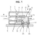
- a connector for a circuit board according to the invention is comprised of at least two kinds of a plurality of male terminal fittings 2 having lengths different from each other and/or from that of the connector housing 1.
- the connector housing 1 is made e.g. of a synthetic resin material to have a substantially block-like shape and is to be closely fixed to the preferably upper surface of a circuit board 5.
- a substantially rectangular tubular receptacle 3 into which an unillustrated mating connector housing is fittable or insertable.
- a plurality of press holes 6 (in this embodiment, five each of press holes 6 are formed on upper and lower levels as shown in FIG.
- terminal support wall 4 preferably substantially closes the tubular receptacle 3 in a longitudinal direction A of the terminal fittings 2 or a mating direction A of the unillustrated mating female connector.
- the male terminal fittings 2 are mounted or mountable by being pressed or inserted or arranged through the respective press holes 6.
- the male terminal fittings 2 mounted on the upper level are substantially longer than those mounted on the lower level.
- the former terminal fittings 2 along a direction of mating A into the receptacle 3 or horizontally project into the receptacle 3, and distal projecting portions thereof serve as engaging portions which are substantially parallel to each other and have the substantially same length. These engaging portions are brought or bringable into contact with unillustrated female terminal fittings being inserted in a mating direction A when the connector housing 1 is engaged with the mating connector housing 1.
- portions 2B of the male terminal fittings 2 projecting outside from the terminal support wall 4 are bent at angles different from 0° or 180°, preferably substantially at right angles in a manner to be described later, and the leading ends thereof serve as mount portions 2A to the circuit board 5.
- the mount portions 2A are inserted into through holes or recesses 7 of the circuit board 5 and secured to the circuit board 5 by unillustrated solder, clamps or the like fixing means.
- the opening edges of the upper press holes 6 and/or the terminal support wall 4 project backward or in a direction away from the receptacle behind the terminal support wall 4 of the connector housing 1, forming restricting projections 8 which receive the supported side of the male terminal fittings 2 over a specified or predetermined or predeterminable length. In this way, the deformation of the male terminal fittings 2 at their supported side (or their side away from their distal projecting portions projecting into the receptacle 3) is prevented.
- a pair of side protection walls 9 and an upper protection wall 10 are so formed as to substantially surround the respective male terminal fittings 2 at a rear part or portion of the connector housing 1.
- These protection walls 9, 10 are so formed as to be substantially in flush with the connector housing 1, and have such lengths that the rear edges thereof are located more outside or backward than the rear edges of the upper male terminal fittings 2.
- the rear part of the connector housing 1 except the rear and lower surfaces is substantially covered by the protection walls 9, 10, thereby preventing the respective terminal fittings 2 from being damaged by an external matter hitting the rear part or projecting part 2B of the terminal fittings 2 from a lateral direction B (FIGS. 1 and 2) or B' (FIG.
- the protection wall 10 preferably protects the projecting portions 2B of the terminal fittings 2 projecting backward from the terminal support wall 4 from being hit or damaged from a direction B substantially opposed to the longitudinal direction of the mount portion 2A of the terminal fittings 2.
- an alignment plate 11 for aligning the mount portions 2A of the respective male terminal fittings 2.
- the alignment plate 11 has a substantially platelike shape and has its side edges engaged with arm portions 12 (FIG. 2) projecting at the bottom and/or lateral portion of the rear surface of the connector housing 1 preferably from below and is held by an unillustrated locking means.
- the alignment plate 11 is formed with positioning holes 13 corresponding to the mount portions 2A of the terminal fittings 2.
- the mount portions 2A are aligned so as to substantially conform to the through holes 7 of the circuit board 5 by being inserted through or fitted in the positioning holes 13.
- An opening at the rear side of the connector housing 1 serves as an insertion space 14 for a jig 15 for bending the male terminal fittings 2.
- the male terminal fittings 2 are bent as shown in FIGS. 3 to 5. Although the bending of the lower male terminal fittings 2 is shown in FIGURES, the upper male terminal fittings 2 are bent in a similar manner by providing a corresponding insertion space 14.
- a bending jig 15 is formed at its leading end with a receiving groove 16 into which the male terminal fitting 2 is at least partially insertable or fittable, and the depth D of the groove 16 at least substantially corresponds to the length L (FIG. 5) between the rear ends of the male terminal fittings 2 and portions 2C thereof to be bent.
- the depth D is substantially equal to the length L.
- the bending jig 15 is rotated or displaced (arrow S2) by an angle different from 0° or 180°, preferably substantially by 90° by hand or an automatic machine. In this way, the male terminal fitting 2 is bent in its set position. If the respective male terminal fittings 2 are repeatedly bent in the aforementioned manner, the terminal fitting bending operation is completed.
- the alignment plate 11 is then secured to the arm portions 12 of the connector housing 1 with the mount portions 2A of the male terminal fittings 2 substantially inserted in the respective positioning holes 13, the connector for the circuit board is assembled. Thereafter, by inserting the mount portions 2A into the through holes 7 of the circuit board 5 and performing soldering or the like, the securing of the connector to the circuit board 5 is completed.
- the alignment plate 11 laterally substantially closes the rear portion of the connector housing 1 such that the terminal fittings 2 do not project outside of the connector housing 1 along a longitudinal direction thereof or a mating direction A (or backward direction).
- the upper protection wall 10 is formed in addition to the side protection walls 9 to surround the respective male terminal filings 2 so as not to project sideways. Accordingly, the deformation of the male terminal fittings 2 by an external matter during the transportation of the connectors can be prevented.
- the alignment interval of the respective mount portions 2A is held proper, eliminating a likelihood that they are brought out of alignment. Therefore, the connector can be smoothly mounted on the circuit board.
Landscapes
- Coupling Device And Connection With Printed Circuit (AREA)
- Connector Housings Or Holding Contact Members (AREA)
- Manufacturing Of Electrical Connectors (AREA)
Applications Claiming Priority (3)
| Application Number | Priority Date | Filing Date | Title |
|---|---|---|---|
| JP17463597A JP3506202B2 (ja) | 1997-06-30 | 1997-06-30 | 基板用コネクタ |
| JP17463597 | 1997-06-30 | ||
| JP174635/97 | 1997-06-30 |
Publications (3)
| Publication Number | Publication Date |
|---|---|
| EP0889559A2 true EP0889559A2 (fr) | 1999-01-07 |
| EP0889559A3 EP0889559A3 (fr) | 1999-12-29 |
| EP0889559B1 EP0889559B1 (fr) | 2003-03-26 |
Family
ID=15982048
Family Applications (1)
| Application Number | Title | Priority Date | Filing Date |
|---|---|---|---|
| EP98112086A Expired - Lifetime EP0889559B1 (fr) | 1997-06-30 | 1998-06-30 | Méthode de fabrication d'un connecteur pour carte imprimée |
Country Status (5)
| Country | Link |
|---|---|
| US (2) | US6068494A (fr) |
| EP (1) | EP0889559B1 (fr) |
| JP (1) | JP3506202B2 (fr) |
| BR (1) | BR9804094A (fr) |
| DE (1) | DE69812483T2 (fr) |
Cited By (2)
| Publication number | Priority date | Publication date | Assignee | Title |
|---|---|---|---|---|
| CN114885497A (zh) * | 2022-05-13 | 2022-08-09 | 苏州三星电子电脑有限公司 | 电子设备 |
| EP4492583A1 (fr) * | 2023-07-11 | 2025-01-15 | TE Connectivity Belgium B.V. | Ensemble pour un connecteur et procédé de fabrication d'un connecteur |
Families Citing this family (26)
| Publication number | Priority date | Publication date | Assignee | Title |
|---|---|---|---|---|
| DE69938321T2 (de) * | 1998-03-26 | 2009-04-30 | Matsushita Electric Works, Ltd., Kadoma | Elektrischer Koppler zur lösbaren Verbindung zwischen Haupteinheit und externer Einheit |
| JP3638840B2 (ja) * | 1999-12-02 | 2005-04-13 | 矢崎総業株式会社 | コネクタの接続方法 |
| JP2002093501A (ja) * | 2000-09-13 | 2002-03-29 | Fci Japan Kk | コネクタ構造、雌コネクタおよび雄コネクタ |
| US6433276B1 (en) * | 2001-03-14 | 2002-08-13 | John Bellora | Surface mount feedthrough |
| EP1417577A4 (fr) * | 2001-08-14 | 2009-08-26 | Verisity Design Inc | Systeme et procede de vcd sur demande |
| EP1418649B1 (fr) * | 2002-11-11 | 2007-08-29 | Sumitomo Wiring Systems, Ltd. | Connecteur |
| JP3736803B2 (ja) | 2002-12-09 | 2006-01-18 | 日本航空電子工業株式会社 | コネクタ、及びコネクタの製造方法 |
| JP2005072385A (ja) * | 2003-08-26 | 2005-03-17 | Sumitomo Wiring Syst Ltd | バスバーのタブとプリント基板の半田接続構造 |
| TWM281314U (en) * | 2005-04-01 | 2005-11-21 | Molex Taiwan Ltd | Electrical connector assembly |
| JP4978774B2 (ja) * | 2006-11-08 | 2012-07-18 | アイシン精機株式会社 | 回転角検出装置の実装構造 |
| JP2008146880A (ja) * | 2006-12-06 | 2008-06-26 | Denso Corp | コネクタ及び電子制御装置 |
| US7815444B2 (en) * | 2007-04-18 | 2010-10-19 | Fci Americas Technology, Inc. | Low profile electrical connector |
| WO2008153485A1 (fr) * | 2007-06-11 | 2008-12-18 | Solibro Research Ab | Traversée électrique |
| JP2009129778A (ja) * | 2007-11-26 | 2009-06-11 | Sumitomo Wiring Syst Ltd | 基板用コネクタ及び電気接続箱 |
| JP2009151940A (ja) | 2007-12-18 | 2009-07-09 | Tyco Electronics Amp Kk | 端子圧入構造および電気コネクタ |
| JP2009151939A (ja) | 2007-12-18 | 2009-07-09 | Tyco Electronics Amp Kk | 端子圧入構造および電気コネクタ |
| CN101335418B (zh) * | 2008-03-05 | 2010-06-02 | 番禺得意精密电子工业有限公司 | 电连接器的组装方法 |
| JP5486885B2 (ja) * | 2009-09-14 | 2014-05-07 | モレックス インコーポレイテド | 電気コネクタおよびコネクタ |
| US8864518B2 (en) * | 2013-01-20 | 2014-10-21 | International Business Machines Corporation | Stack connector component having high speed and low speed pins |
| US9431751B2 (en) * | 2014-03-25 | 2016-08-30 | Tyco Electronics Brasil Ltda | Connector having a pin guide for use with a printed circuit board |
| JP2016018595A (ja) * | 2014-07-04 | 2016-02-01 | タイコエレクトロニクスジャパン合同会社 | 電気コネクタ |
| DE202015101799U1 (de) * | 2015-04-13 | 2016-07-14 | Fct Electronic Gmbh | Steckermodul für einen elektrischen Rechtecksteckverbinder und Rechtecksteckverbinder mit einem solchen Steckermodul |
| US9865949B2 (en) * | 2015-04-28 | 2018-01-09 | Denso Corporation | Electronic device and connector |
| JP6660552B2 (ja) * | 2015-11-06 | 2020-03-11 | 住友電装株式会社 | コネクタ |
| WO2018163247A1 (fr) * | 2017-03-06 | 2018-09-13 | 三菱電機株式会社 | Unité de commande ayant une structure à ajustement par pression |
| JP2024107885A (ja) * | 2023-01-30 | 2024-08-09 | 住友電装株式会社 | コネクタ |
Family Cites Families (15)
| Publication number | Priority date | Publication date | Assignee | Title |
|---|---|---|---|---|
| US4488355A (en) * | 1982-06-30 | 1984-12-18 | At&T Technologies, Inc. | Methods of and apparatus for forming contact elements in a cord coupler housing |
| US4491376A (en) * | 1982-09-20 | 1985-01-01 | General Motors Corporation | Electrical header assembly |
| US4697864A (en) * | 1986-06-19 | 1987-10-06 | Amp Incorporated | Printed circuit board receptacle for sealed connector |
| US4859198A (en) * | 1988-08-25 | 1989-08-22 | Gte Products Corporation | Contact assembly |
| US4966556A (en) * | 1989-06-13 | 1990-10-30 | General Datacomm, Inc. | Electrical connector for direct connection to plated through holes in circuit board |
| JP2575617Y2 (ja) * | 1993-01-14 | 1998-07-02 | 矢崎総業株式会社 | 回路基板用コネクタ |
| NL9302227A (nl) * | 1993-12-21 | 1995-07-17 | Connector Systems Tech Nv | Elektrische connector met een de aansluitpennen positionerend lichaam. |
| US5511984A (en) * | 1994-02-08 | 1996-04-30 | Berg Technology, Inc. | Electrical connector |
| US5490787A (en) * | 1994-08-29 | 1996-02-13 | The Whitaker Corporation | Electrical connector with integral supporting structure |
| JPH08315930A (ja) * | 1995-05-17 | 1996-11-29 | Sumitomo Wiring Syst Ltd | コネクタ |
| US5676554A (en) * | 1995-03-28 | 1997-10-14 | Sumitomo Wiring Systems, Ltd. | Board mounted connector |
| JP2874586B2 (ja) * | 1995-03-28 | 1999-03-24 | 住友電装株式会社 | 基板装着コネクタ |
| FR2733363B1 (fr) * | 1995-04-21 | 1997-05-30 | Framatome Connectors France | Procede de realisation d'un element modulaire de connexion electrique et element modulaire de connexion electrique ainsi obtenu |
| JPH09320706A (ja) * | 1996-05-28 | 1997-12-12 | Yazaki Corp | プリント基板用コネクタ |
| US5863222A (en) * | 1997-06-03 | 1999-01-26 | The Whitaker Corporation | Shielded electrical connector |
-
1997
- 1997-06-30 JP JP17463597A patent/JP3506202B2/ja not_active Expired - Fee Related
-
1998
- 1998-06-02 US US09/088,882 patent/US6068494A/en not_active Expired - Lifetime
- 1998-06-29 BR BR9804094-4A patent/BR9804094A/pt not_active Application Discontinuation
- 1998-06-30 EP EP98112086A patent/EP0889559B1/fr not_active Expired - Lifetime
- 1998-06-30 DE DE69812483T patent/DE69812483T2/de not_active Expired - Lifetime
-
1999
- 1999-05-07 US US09/307,212 patent/US6161283A/en not_active Expired - Lifetime
Cited By (3)
| Publication number | Priority date | Publication date | Assignee | Title |
|---|---|---|---|---|
| CN114885497A (zh) * | 2022-05-13 | 2022-08-09 | 苏州三星电子电脑有限公司 | 电子设备 |
| US12363828B2 (en) | 2022-05-13 | 2025-07-15 | Samsung Electronics Co., Ltd. | Electronic device |
| EP4492583A1 (fr) * | 2023-07-11 | 2025-01-15 | TE Connectivity Belgium B.V. | Ensemble pour un connecteur et procédé de fabrication d'un connecteur |
Also Published As
| Publication number | Publication date |
|---|---|
| EP0889559A3 (fr) | 1999-12-29 |
| JPH1126058A (ja) | 1999-01-29 |
| DE69812483T2 (de) | 2004-01-29 |
| BR9804094A (pt) | 1999-12-21 |
| US6161283A (en) | 2000-12-19 |
| JP3506202B2 (ja) | 2004-03-15 |
| DE69812483D1 (de) | 2003-04-30 |
| US6068494A (en) | 2000-05-30 |
| EP0889559B1 (fr) | 2003-03-26 |
Similar Documents
| Publication | Publication Date | Title |
|---|---|---|
| US6068494A (en) | Connector for circuit board and method for producing a connector | |
| US6866523B2 (en) | Construction for mounting a terminal, a circuit board connector and method of mounting it | |
| EP1936749B1 (fr) | Organe de contact, connecteur et procédé de fabrication | |
| KR100216002B1 (ko) | 단자의완전한삽입을용이하게하는단자위치확정장치를구비한전기커넥터 | |
| JP3368471B2 (ja) | 電気コネクタ | |
| JP2896738B2 (ja) | コネクタ | |
| US7033229B2 (en) | Terminal fitting and a connector | |
| EP1286424A2 (fr) | Connecteur électrique ayant des pièces surmoulées et encliquetées | |
| US7588446B2 (en) | Connector and a connector assembly | |
| CN101361235A (zh) | 电连接器组件 | |
| US6767239B2 (en) | Connector with interengageable rib and groove for guiding connection and a method of assembling such a connector | |
| AU711843B2 (en) | A coaxial connector and method for fixing this connector to a circuit board | |
| US6767259B2 (en) | Terminal fitting with outwardly projecting engagement portion for engaging a resin lock and a method of forming the terminal fitting | |
| EP1557908A2 (fr) | Un connecteur | |
| US6729915B2 (en) | Connector for circuit board and method of assembling it | |
| JPH07307186A (ja) | 端子保護板を備えたコネクタ | |
| US7134910B2 (en) | Circuit board connector | |
| EP0884809B1 (fr) | Connecteur pour carte de circuit imprimé | |
| JPH07230844A (ja) | 雌型端子 | |
| JP3331412B2 (ja) | 基板スルーホール接続用コンタクトおよびコネクタ | |
| JPH09147960A (ja) | 汎用コネクタ及びその結合方法 | |
| EP1150388B1 (fr) | Construction pour la prévention de tremblement d'une borne de contact et connecteur | |
| US7165993B2 (en) | Connector and method of molding a connector | |
| US6488547B2 (en) | Connector with longitudinally spaced locks for retaining terminal fittings | |
| JP2002042935A (ja) | コネクタ |
Legal Events
| Date | Code | Title | Description |
|---|---|---|---|
| PUAI | Public reference made under article 153(3) epc to a published international application that has entered the european phase |
Free format text: ORIGINAL CODE: 0009012 |
|
| 17P | Request for examination filed |
Effective date: 19980724 |
|
| AK | Designated contracting states |
Kind code of ref document: A2 Designated state(s): DE FR GB IT |
|
| AX | Request for extension of the european patent |
Free format text: AL;LT;LV;MK;RO;SI |
|
| PUAL | Search report despatched |
Free format text: ORIGINAL CODE: 0009013 |
|
| AK | Designated contracting states |
Kind code of ref document: A3 Designated state(s): AT BE CH CY DE DK ES FI FR GB GR IE IT LI LU MC NL PT SE |
|
| AX | Request for extension of the european patent |
Free format text: AL;LT;LV;MK;RO;SI |
|
| RIC1 | Information provided on ipc code assigned before grant |
Free format text: 6H 01R 23/70 A, 6H 01R 43/20 B |
|
| AKX | Designation fees paid |
Free format text: DE FR GB IT |
|
| 17Q | First examination report despatched |
Effective date: 20010606 |
|
| GRAG | Despatch of communication of intention to grant |
Free format text: ORIGINAL CODE: EPIDOS AGRA |
|
| RTI1 | Title (correction) |
Free format text: METHOD FOR PRODUCING A CONNECTOR FOR A CIRCUIT BOARD |
|
| GRAG | Despatch of communication of intention to grant |
Free format text: ORIGINAL CODE: EPIDOS AGRA |
|
| GRAH | Despatch of communication of intention to grant a patent |
Free format text: ORIGINAL CODE: EPIDOS IGRA |
|
| GRAH | Despatch of communication of intention to grant a patent |
Free format text: ORIGINAL CODE: EPIDOS IGRA |
|
| GRAA | (expected) grant |
Free format text: ORIGINAL CODE: 0009210 |
|
| AK | Designated contracting states |
Designated state(s): DE FR GB IT |
|
| PG25 | Lapsed in a contracting state [announced via postgrant information from national office to epo] |
Ref country code: IT Free format text: LAPSE BECAUSE OF FAILURE TO SUBMIT A TRANSLATION OF THE DESCRIPTION OR TO PAY THE FEE WITHIN THE PRESCRIBED TIME-LIMIT;WARNING: LAPSES OF ITALIAN PATENTS WITH EFFECTIVE DATE BEFORE 2007 MAY HAVE OCCURRED AT ANY TIME BEFORE 2007. THE CORRECT EFFECTIVE DATE MAY BE DIFFERENT FROM THE ONE RECORDED. Effective date: 20030326 Ref country code: FR Free format text: LAPSE BECAUSE OF FAILURE TO SUBMIT A TRANSLATION OF THE DESCRIPTION OR TO PAY THE FEE WITHIN THE PRESCRIBED TIME-LIMIT Effective date: 20030326 |
|
| REG | Reference to a national code |
Ref country code: GB Ref legal event code: FG4D |
|
| RIC1 | Information provided on ipc code assigned before grant |
Ipc: 7H 01R 43/20 B Ipc: 7H 01R 12/20 B Ipc: 7H 01R 12/18 A |
|
| REF | Corresponds to: |
Ref document number: 69812483 Country of ref document: DE Date of ref document: 20030430 Kind code of ref document: P |
|
| PG25 | Lapsed in a contracting state [announced via postgrant information from national office to epo] |
Ref country code: GB Free format text: LAPSE BECAUSE OF NON-PAYMENT OF DUE FEES Effective date: 20030630 |
|
| PLBE | No opposition filed within time limit |
Free format text: ORIGINAL CODE: 0009261 |
|
| STAA | Information on the status of an ep patent application or granted ep patent |
Free format text: STATUS: NO OPPOSITION FILED WITHIN TIME LIMIT |
|
| GBPC | Gb: european patent ceased through non-payment of renewal fee |
Effective date: 20030630 |
|
| EN | Fr: translation not filed | ||
| 26N | No opposition filed |
Effective date: 20031230 |
|
| PGFP | Annual fee paid to national office [announced via postgrant information from national office to epo] |
Ref country code: DE Payment date: 20120627 Year of fee payment: 15 |
|
| REG | Reference to a national code |
Ref country code: DE Ref legal event code: R119 Ref document number: 69812483 Country of ref document: DE |
|
| PG25 | Lapsed in a contracting state [announced via postgrant information from national office to epo] |
Ref country code: DE Free format text: LAPSE BECAUSE OF NON-PAYMENT OF DUE FEES Effective date: 20140101 |
|
| REG | Reference to a national code |
Ref country code: DE Ref legal event code: R079 Ref document number: 69812483 Country of ref document: DE Free format text: PREVIOUS MAIN CLASS: H01R0012180000 Ipc: H01R0012500000 |
|
| REG | Reference to a national code |
Ref country code: DE Ref legal event code: R119 Ref document number: 69812483 Country of ref document: DE Effective date: 20140101 Ref country code: DE Ref legal event code: R079 Ref document number: 69812483 Country of ref document: DE Free format text: PREVIOUS MAIN CLASS: H01R0012180000 Ipc: H01R0012500000 Effective date: 20140925 |