EP0890845B1 - Circuit et procédé de mesure du rapport signal/bruit - Google Patents
Circuit et procédé de mesure du rapport signal/bruit Download PDFInfo
- Publication number
- EP0890845B1 EP0890845B1 EP19980112863 EP98112863A EP0890845B1 EP 0890845 B1 EP0890845 B1 EP 0890845B1 EP 19980112863 EP19980112863 EP 19980112863 EP 98112863 A EP98112863 A EP 98112863A EP 0890845 B1 EP0890845 B1 EP 0890845B1
- Authority
- EP
- European Patent Office
- Prior art keywords
- circuit
- output
- electric power
- signal
- value
- Prior art date
- Legal status (The legal status is an assumption and is not a legal conclusion. Google has not performed a legal analysis and makes no representation as to the accuracy of the status listed.)
- Expired - Lifetime
Links
- 238000000034 method Methods 0.000 title claims description 12
- 238000012935 Averaging Methods 0.000 claims description 38
- 238000006243 chemical reaction Methods 0.000 claims description 32
- 238000005259 measurement Methods 0.000 claims description 11
- 238000005070 sampling Methods 0.000 claims description 8
- 238000004891 communication Methods 0.000 claims description 7
- 238000010586 diagram Methods 0.000 description 5
- 230000003247 decreasing effect Effects 0.000 description 2
- 238000005516 engineering process Methods 0.000 description 2
- 238000012544 monitoring process Methods 0.000 description 2
- 230000005540 biological transmission Effects 0.000 description 1
- 230000001413 cellular effect Effects 0.000 description 1
- 238000012937 correction Methods 0.000 description 1
- 230000001419 dependent effect Effects 0.000 description 1
- 238000010295 mobile communication Methods 0.000 description 1
Images


Classifications
-
- H—ELECTRICITY
- H04—ELECTRIC COMMUNICATION TECHNIQUE
- H04W—WIRELESS COMMUNICATION NETWORKS
- H04W52/00—Power management, e.g. Transmission Power Control [TPC] or power classes
- H04W52/04—Transmission power control [TPC]
- H04W52/18—TPC being performed according to specific parameters
- H04W52/24—TPC being performed according to specific parameters using SIR [Signal to Interference Ratio] or other wireless path parameters
-
- G—PHYSICS
- G01—MEASURING; TESTING
- G01R—MEASURING ELECTRIC VARIABLES; MEASURING MAGNETIC VARIABLES
- G01R29/00—Arrangements for measuring or indicating electric quantities not covered by groups G01R19/00 - G01R27/00
- G01R29/26—Measuring noise figure; Measuring signal-to-noise ratio
-
- H—ELECTRICITY
- H04—ELECTRIC COMMUNICATION TECHNIQUE
- H04W—WIRELESS COMMUNICATION NETWORKS
- H04W52/00—Power management, e.g. Transmission Power Control [TPC] or power classes
- H04W52/04—Transmission power control [TPC]
- H04W52/06—TPC algorithms
- H04W52/08—Closed loop power control
-
- Y—GENERAL TAGGING OF NEW TECHNOLOGICAL DEVELOPMENTS; GENERAL TAGGING OF CROSS-SECTIONAL TECHNOLOGIES SPANNING OVER SEVERAL SECTIONS OF THE IPC; TECHNICAL SUBJECTS COVERED BY FORMER USPC CROSS-REFERENCE ART COLLECTIONS [XRACs] AND DIGESTS
- Y02—TECHNOLOGIES OR APPLICATIONS FOR MITIGATION OR ADAPTATION AGAINST CLIMATE CHANGE
- Y02D—CLIMATE CHANGE MITIGATION TECHNOLOGIES IN INFORMATION AND COMMUNICATION TECHNOLOGIES [ICT], I.E. INFORMATION AND COMMUNICATION TECHNOLOGIES AIMING AT THE REDUCTION OF THEIR OWN ENERGY USE
- Y02D30/00—Reducing energy consumption in communication networks
- Y02D30/70—Reducing energy consumption in communication networks in wireless communication networks
Definitions
- the present invention relates to a S/N measuring circuit for a transmitting electric power control apparatus used in a digital mobile communicating system.
- transmitting electric power control is used for suppressing consumption of electric power at a mobile station while maintaining reception quality at a desired value, and for avoiding unnecessary interference with other mobile stations.
- the transmitting electric power control is essential.
- a Signal-to-Noise Power Ratio (referred to as an S/N, hereinafter) is measured from a signal received and demodulated at a base station, instruction is sent to the mobile station so that this S/N value will be a value enough for desired reception quality, and transmitting electric power is sequentially controlled.
- a noise N used here includes a thermal noise and an interference signal.
- US 5 278 992 A which discloses a digital cordless phone system
- the power of a remote transmitted signal is controlled by a remote communication device.
- the remote communication device communicates with the base communication device.
- the base communication device transmits to the remote device a base transmitted signal.
- the base transmitted signal is received by the remote device and its power is measured.
- Fig. 4 is a view showing an S/N measuring circuit of the first prior art.
- an S/N measuring circuit 50 of the first prior art is constructed of a modulation removing circuit 3 connected to an analog-digital (A/D) converter 2, a first averaging circuit 4, a first square operating circuit 5, a second square operating circuit 6 connected to the analog-digital (A/D) converter 2, a second averaging circuit 7, a subtracting circuit 8, and a dividing circuit 9.
- a demodulated reception signal is sampled at a modulation clock by the A/D converter 2.
- the S/N measuring circuit after a modulated component of an output of the A/D converter 2 is removed in the modulation removing circuit 3, the output is averaged over a plurality of symbol sections in the first averaging circuit 4, and an amplitude value in which a noise component is suppressed is obtained.
- An output of the first averaging circuit 4 is squared by the first square operating circuit 5, and desired signal power S is obtained.
- an output of the A/D converter 2 is supplied to the second square operating circuit 6, and is converted into time series having a dimension of electric power. Thereafter, the output is averaged over a plurality of symbol sections by the second averaging circuit 7, and total electric power P of demodulated signals is obtained.
- the subtracting circuit 8 obtains noise electric power N by subtracting the desired signal power S from the total electric power P of the demodulated signals.
- the dividing circuit 9 receives the obtained S and N as above, and calculates a ratio S/N thereof.
- a noise component superimposed over a demodulated signal shows a Gaussian distribution of which center is at the amplitude A of the signal point in the absence of the noise, and the noise electric power N is given by the following equation (3):
- Fig. 5 is a view showing a conventional transmitting electric power control apparatus using the S/N measuring circuit shown in Fig. 4.
- a base station 51 includes a demodulator 11 connected to an antenna, a decoder 12, a target S/N control circuit 52, an adder 13, a decision device 14, a TPC bit generating circuit 15, and a transmitter 16 connected to an antenna.
- the target S/N control circuit 52 includes a reception quality measuring circuit 61, an adder 62, a decision device 63 and a target S/N determining circuit 64.
- a mobile station 53 includes a demodulator 21 connected to an antenna, a TPC bit decoder 22, a transmitting electric power determining circuit 23, a transmitter 24, and an encoder 25.
- demodulated signals demodulated by the demodulator 11 are sampled at a modulation clock by the A/D converter 2.
- a series of sampled values of the demodulated signals that are outputs of the A/D converter 2 are input to the decoder 12, and information signals after the decoding are obtained.
- an output of the A/D converter 2 is supplied to the S/N measuring circuit 50.
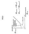
- the S/N measuring circuit 50 has the same arrangement as the S/N measuring circuit 50 shown in Fig. 4, and in the S/N measuring circuit, a non-linear bias in which a measured S/N value appears higher is observed as the received S/N is lower.
- the reception quality measuring circuit 61 receives an information signal decoded in the decoder 12, and measures reception quality.
- the adder 62 obtains a difference between the reception quality measured by the reception quality measuring circuit 61 and target reception quality, and supplies the difference to the decision device 63.
- the decision device 63 determines an amount of increase or decrease of the target S/N based on the output from the adder 62.
- the target S/N determining circuit 64 determines the target S/N based on the amount of the increase or decrease of the target S/N determined by the decision device 63.
- the adder 13 calculates a difference between the measured S/N output from the S/N measuring circuit 50 and the target S/N output from the target S/N determining circuit 64, and supplies the difference to the decision device 14.
- the decision device 14 determines an amount of increase or decrease of transmitting electric power to the mobile station 53 based on the output from the adder 13.
- the amount of increase or decrease of the transmitting electric power determined by the decision device 14 is converted into a bit by the TPC bit generating circuit 15, and is transmitted to the mobile station by the transmitter 16.
- the demodulator 21 demodulates a signal transmitted by the base station 51.
- a demodulated signal that is an output from the demodulator 21 is input to the TPC bit decoder 22, and the TPC bit decoder decodes the TPC bit generated in the base station 51.
- the decoded TPC bit is input to the transmitting electric power determining circuit 23, and transmitting electric power of the mobile station 53 is determined.
- the transmitter 24 transmits an information signal encoded by the encoder 25.
- the objective of the present invention is to solve the above-mentioned tasks.
- the objective of the present invention is to provide an S/N measuring circuit and method capable of conducting S/N measurement with high accuracy.
- Another objective of an embodiment of the present invention is to provide a transmitting electric power control apparatus capable of simply conducting transmitting electric power control with high accuracy using the above-described S/N measuring circuit.
- yet another objective of an embodiment of the present invention is to provide a digital mobile communicating system including the above-described transmitting electric power control apparatus, and a base station thereof.
- an S/N measuring circuit which includes a modulation removing circuit, connected to an A/D converter for receiving a signal demodulated from a digital modulated signal and sampling the demodulated signal at a modulation clock, for removing data modulation by multiplying a sampled value of a demodulated signal that is an output from the above-described A/D converter by a decision symbol signal, a first averaging circuit for averaging an output from the above-described modulation removing circuit over a plurality of symbol sections to suppress a noise superimposed over the demodulated signal, a first square operating circuit for squaring an output from the above-described first averaging circuit to obtain a desired signal power, a second square operating circuit for applying square operation to the sampled value of the demodulated signal that is an output from the above-described A/D converter, a second averaging circuit for averaging an output from the above-described second square operating circuit over a plurality of symbol sections to obtain total electric power
- the above-described S/N measuring circuit is provided, wherein the above-described table conversion circuit removes a non-linear bias occurred from a symbol error in case that the S/N value output from the above-described dividing circuit is small by providing characteristic by means of the above-described conversion table, which is the reverse of characteristic previously obtained by measurement of a corresponding relation between the S/N value output from the above-described dividing circuit and an actual S/N value of the demodulated signal.
- a transmitting electric power control apparatus for controlling transmitting electric power of an information signal transmitted to a base station from a mobile station
- the above-described base station has a demodulator for receiving a digital modulated and coded information signal and conducting demodulation, an A/D converter for sampling an output from the above-described demodulator at a modulation clock, a decoder for decoding a demodulated signal that is an output from the above-described A/D converter and outputting an information signal, a modulation removing circuit for removing data modulation by multiplying a sampled value of the demodulated signal that is an output from the above-described A/D converter by a decision symbol signal, a first averaging circuit for averaging an output from the above-described modulation removing circuit over a plurality of symbol sections to suppress a noise superimposed over the demodulated signal, a first square operating circuit for squaring an output from the above-described first a
- the above-described transmitting electric power control apparatus wherein the above-described table conversion circuit removes a non-linear bias occurred from a symbol error in case that the S/N value output from the above-described dividing circuit is small by providing characteristic by means of the above-described conversion table, which is the reverse of characteristic previously obtained by measurement of a corresponding relation between the S/N value output from the above-described dividing circuit and an actual S/N value of the demodulated signal.
- a base station of a digital mobile communicating system for conducting communication while controlling transmitting electric power of an information signal transmitted to the base station from a mobile station
- the base station has a demodulator for receiving a digital modulated and coded information signal and conducting demodulation, an A/D converter for sampling an output from the above-described demodulator at a modulation clock, a decoder for decoding a demodulated signal that is an output from the above-described A/D converter and outputting an information signal, a modulation removing circuit for removing data modulation by multiplying a sampled value of the demodulated signal that is an output from the above-described A/D converter by a decision symbol signal, a first averaging circuit for averaging an output from the above-described modulation removing circuit over a plurality of symbol sections to suppress a noise superimposed over the demodulated signal, a first square operating circuit for squaring an output from the above-described first
- a digital mobile communicating system including the above-described base station and the above-described mobile station
- the above-described mobile station has a demodulator for receiving a digital modulated TPC signal and conducting demodulation, a TPC bit decoder for deciding a TPC bit from an output from the above-described demodulator, a transmitting electric power determining circuit for receiving the TPC bit that is an output from the above-described TPC bit decoder and determining transmitting electric power of the mobile station, and a transmitter for transmitting a coded information signal based on the transmitting electric power determined by the above-described transmitting electric power determining circuit.
- an S/N measuring method includes steps of (a) removing data modulation by multiplying a sampled value of a demodulated signal that is an output from an A/D converter by a decision symbol signal, the A/D converter receiving a signal demodulated from a digital modulated signal and sampling the demodulated signal at a modulation clock, (b) averaging the demodulated signal in which the data modulation is removed over a plurality of symbol sections to suppress a noise superimposed over the demodulated signal, (c) squaring the averaged signal to obtain a desired signal power, (d) applying square operation to the sampled value of the demodulated signal that is an output from the A/D converter, (e) averaging the squared value over a plurality of symbol sections to obtain total electric power of the demodulated signal, (f) subtracting the desired signal power from the total electric power to obtain noise electric power, (g) receiving the desired signal power and the noise electric power, and calculating an S
- the step (h) includes a step of removing a non-linear bias occurred from a symbol error in case that the S/N value is small by providing characteristic by means of the conversion table, which is the reverse of characteristic previously obtained by measurement of a corresponding relation between the S/N value and an actual S/N value of the demodulated signal.
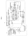
- Fig. 1 is a view showing an S/N measuring circuit in an embodiment of the present invention.
- an S/N measuring circuit 10 in the embodiment of the present invention includes a modulation removing circuit 3 connected to an A/D converter 2, a first averaging circuit 4, a first square operating circuit 5, a second square operating circuit 6 connected to the A/D converter 2, a second averaging circuit 7, a subtracting circuit 8, and a dividing circuit 9, and this arrangement is the same as the first prior art shown in Fig. 4.
- the S/N measuring circuit 10 in the embodiment of the present invention further includes a table conversion circuit 1.
- a demodulated reception signal is sampled at a modulation clock by the A/D converter 2.
- a series of sampled values of a modulated signal that is an output from the A/D converter 2 are averaged over a plurality of symbol sections in the first averaging circuit 4, after a modulated component thereof is removed in the modulation removing circuit 3, and an amplitude value in which a noise component is suppressed is obtained.
- An output of this averaging circuit 4 is squared by the first square operating circuit 5, and desired signal power S is obtained.
- an output of the A/D converter 2 is supplied to the second square operating circuit 6, and is converted into time series having a dimension of electric power. Thereafter, the output is averaged over a plurality of symbol sections by the second averaging circuit 7, and total electric power P of demodulated signals is obtained.
- the subtracting circuit 8 obtains noise electric power N by subtracting the desired signal power S from the total electric power P of the demodulated signals.
- the table conversion circuit 1 is provided behind the dividing circuit 9, and converts an S/N output from the dividing circuit 9 and outputs it.
- characteristic that is the reverse of non-linear bias characteristic of the S/N output from the dividing circuit 9 is stored as a table, and the table conversion circuit instantly outputs an S/N value in which a bias is corrected. Thereby, correct S/N measurement becomes to be possible.
- Fig. 3 is a block diagram showing a transmitting electric power control apparatus using the S/N measuring circuit 10 in Fig. 1.
- a base station 20 includes an A/D converter 2.
- an S/N measuring circuit 10 a demodulator 11 connected to an antenna, a decoder 12, an adder 13, a decision device 14, a TPC bit generating circuit 15, and a transmitter 16 connected to an antenna.
- a mobile station 53 like the prior art includes a demodulator 21, a TPC bit decoder 22, a transmitting electric power determining circuit 23, a transmitter 24, and an encoder 25.
- the S/N measuring circuit 10 shown in Fig. 1 has the same arrangement as the S/N measuring circuit 10 shown in Fig. 1, and has a function in which a corrected and accurate S/N value is measured from the sampled value of the demodulated signal and output.
- the adder 13 a difference between a measured S/N that is an output from the S/N measuring circuit 10 and a preset control target S/N of transmitting electric power is calculated and supplied to the decision device 14.
- the decision device 14 determines an amount of increase or decrease of the transmitting electric power to the mobile station 53, based on an output from the adder 13.
- the determined amount of the increase or decrease of the transmitting electric power is converted into a bit by the TPC bit generating circuit 15, and is transmitted to the mobile station 20 by the transmitter 16.
- the demodulator 21 receives a signal transmitted by the base station and conducts demodulation.
- a demodulated signal that is an output from the demodulator 21 is input to the TPC bit decoder 22, and the TPC bit decoder decodes the TPC bit generated in the base station 20.
- the TPC bit decoded in the TPC bit decoder 22 is input to the transmitting electric power determining circuit 23, and transmitting electric power of the mobile station 53 is determined.
- the transmitter 24 transmits a coded information signal.
- non-linear bias characteristic in the S/N measurement is previously obtained by measurement, the conversion table for realizing this reverse characteristic is created, and when a measured S/N value is output from the dividing circuit, the table conversion circuit receives this S/N value as an input and outputs a corrected S/N value from the above-described conversion table. Therefore, it is possible to provide the S/N measuring circuit capable of measuring the S/N with high accuracy.
- the above-described corrected and measured S/N is compared with the target S/N in the base station, and the base station transmits a demand for increasing and decreasing the transmitting electric power to the mobile station, and, in accordance with the instruction from the base station, the transmitting electric power is determined in the mobile station.
- the apparatus since the outer-loop for correcting an S/N measuring bias is not necessary, a scale of the apparatus becomes to be small. Also, since the apparatus can cope with a fast change of the received S/N, it is possible to provide the transmitting electric power control apparatus capable of conducting the transmitting electric power control with high accuracy.
Landscapes
- Physics & Mathematics (AREA)
- General Physics & Mathematics (AREA)
- Engineering & Computer Science (AREA)
- Computer Networks & Wireless Communication (AREA)
- Signal Processing (AREA)
- Mobile Radio Communication Systems (AREA)
- Digital Transmission Methods That Use Modulated Carrier Waves (AREA)
Claims (8)
- Circuit de mesure du rapport S/B comprenant :un circuit de suppression de modulation (3), connecté à un convertisseur A/N pour recevoir un signal démodulé à partir d'un signal numérique modulé et échantillonner ledit signal démodulé à une horloge de modulation, pour supprimer la modulation des données en multipliant une valeur échantillonnée d'un signal démodulé qui est un signal de sortie dudit convertisseur A/N par un signal symbole de décision ;un premier circuit de production de valeurs moyennes (4) pour produire la moyenne d'un signal de sortie dudit circuit de suppression de modulation sur une pluralité de sections de symbole pour supprimer un bruit superposé sur ledit signal démodulé ;un premier circuit de mise au carré (5) pour mettre au carré un signal de sortie dudit premier circuit de production de valeurs moyennes pour obtenir une puissance de signal désirée ;un deuxième circuit de mise au carré (6) pour appliquer une opération de mise au carré à ladite valeur échantillonnée dudit signal démodulé qui est un signal de sortie dudit convertisseur A/N ;un deuxième circuit de production de valeurs moyennes (7) pour produire la moyenne d'un signal de sortie dudit deuxième circuit de mise au carré sur une pluralité de sections de symbole pour obtenir la puissance électrique totale dudit signal démodulé ;un circuit de soustraction (8) pour soustraire ladite puissance de signal désirée qui est un signal de sortie dudit premier circuit de mise au carré à partir de ladite puissance électrique totale dudit signal démodulé qui est un signal de sortie dudit deuxième circuit de production de valeurs moyennes pour obtenir la puissance électrique du bruit ;un circuit diviseur (9) pour recevoir ladite puissance de signal désirée qui est un signal de sortie dudit premier circuit de mise au carré et ladite puissance électrique du bruit qui est un signal de sortie dudit circuit de soustraction, et calculer une valeur S/B ; etun circuit de conversion de table (1) pour recevoir ladite valeur S/B sortie dudit circuit de division et produire une valeur S/B corrigée conformément à une table de conversion prédéterminée.
- Circuit de mesure du rapport S/B selon la revendication 1, dans lequel ledit circuit de conversion de table (1) supprime une polarisation non linéaire due à une erreur de symbole au cas où ladite valeur S/B produite à partir dudit circuit de division est faible, en proposant une caractéristique au moyen de ladite table de conversion, qui est l'inverse d'une caractéristique précédemment obtenue par mesure d'un rapport correspondant entre ladite valeur S/B produite à partir dudit circuit de division et une valeur S/B réelle dudit signal démodulé.
- Appareil de contrôle de puissance électrique d'émission pour contrôler la puissance électrique d'émission d'un signal d'information transmis à une station de base (20) à partir d'une station mobile (53), dans lequel
ladite station de base (20) comprend :et dans lequelun démodulateur (11) pour recevoir un signal d'information numérique modulé et codé et effectuer la démodulation ;un convertisseur A/N (2) pour échantillonner un signal de sortie dudit démodulateur à une horloge de modulation ;un décodeur (12) pour décoder un signal démodulé qui est un signal de sortie dudit convertisseur A/N et produisant un signal d'information ;le circuit de mesure du rapport S/B de la revendication 1 ;un additionneur (13) pour obtenir une différence entre un rapport S/B mesuré qui est un signal de sortie dudit circuit de conversion de table et un rapport S/B cible qui est une valeur cible de contrôle de puissance électrique d'émission ;un dispositif de décision (14) pour déterminer une quantité d'augmentation ou de diminution de ladite puissance électrique d'émission, qui est appliquée à ladite station mobile, à partir de ladite différence entre ledit rapport S/B mesuré et ledit rapport S/B cible, qui est un signal de sortie dudit additionneur ;un circuit générateur de bits TPC (15) pour convertir un résultat de sortie à partir dudit dispositif de décision en un bit ; etun émetteur (16) pour transmettre un bit TPC déterminé dans ledit circuit générateur de bits TPC à ladite station mobile,
ladite station mobile (53) comprend :un démodulateur (21) pour recevoir un signal numérique TPC modulé et effectuer une démodulation ;un décodeur de bits TPC (22) pour décoder un bit TPC à partir d'un signal de sortie dudit démodulateur ;un circuit déterminant la puissance électrique d'émission (23) pour recevoir ledit bit TPC qui est un signal de sortie dudit décodeur de bits TPC et déterminant la puissance électrique d'émission de ladite station mobile ; etun émetteur (24) pour émettre un signal d'information codé basé sur ladite puissance électrique d'émission déterminée par ledit circuit déterminant la puissance électrique d'émission. - Appareil de contrôle de la puissance électrique d'émission selon la revendication 3, dans lequel ledit circuit de conversion de table (1) supprime une polarisation non linéaire due à une erreur de symbole au cas où ladite valeur S/B produite dudit circuit de division est faible, en proposant une caractéristique au moyen de ladite table de conversion, qui est l'inverse d'une caractéristique précédemment obtenue par mesure d'un rapport correspondant entre ladite valeur S/B produite à partir dudit circuit de division et une valeur S/B réelle dudit signal démodulé.
- Station de base d'un système numérique de communication mobile pour effectuer une communication tout en contrôlant la puissance électrique d'émission d'un signal d'information transmis à ladite station de base à partir d'une station mobile, ladite station de base comprenant :un démodulateur (11) pour recevoir un signal d'information numérique modulé et codé et effectuer une démodulation ;un convertisseur A/N (2) pour échantillonner un signal de sortie dudit démodulateur à une horloge de modulation ;un décodeur (12) pour décoder un signal démodulé qui est un signal de sortie dudit convertisseur A/N et produisant un signal d'information ;le circuit de mesure du rapport S/B de la revendication 1 ou 2 ;un additionneur (13) pour obtenir une différence entre un rapport S/B mesuré qui est un signal de sortie dudit circuit de conversion de table et un rapport S/B cible qui est une valeur cible de contrôle de puissance électrique d'émission ;un dispositif de décision (14) pour déterminer une quantité d'augmentation ou de diminution de ladite puissance électrique d'émission, qui est appliquée à ladite station mobile, à partir de ladite différence entre ledit rapport S/B mesuré et ledit rapport S/B cible, qui est un signal de sortie dudit additionneur ;un circuit générateur de bits TPC (15) pour convertir un résultat émis dudit dispositif de décision en un bit ; etun émetteur (16) pour émettre un bit TPC déterminé dans ledit circuit générateur de bits TPC à ladite station mobile.
- Système de communication mobile numérique comprenant :dans lequelune station de base (20, 51) citée dans la revendication 5 ; etune station mobile (53) citée dans la revendication 5,
ladite station mobile (53) comprend :un démodulateur (21) pour recevoir un signal numérique TPC modulé et effectuer une démodulation ;un décodeur de bits TPC (22) pour décoder un bit TPC à partir d'un signal de sortie dudit démodulateur ;un circuit déterminant la puissance électrique d'émission (23) pour recevoir ledit bit TPC qui est un signal de sortie dudit décodeur de bits TPC et déterminant la puissance électrique d'émission de ladite station mobile ; etun émetteur (24) pour émettre un signal d'information codé basé sur ladite puissance électrique d'émission déterminée par ledit circuit déterminant la puissance électrique d'émission. - Procédé de mesure du rapport S/B comprenant les étapes consistant à :(a) supprimer la modulation de données en multipliant une valeur échantillonnée d'un signal démodulé qui est un signal de sortie d'un convertisseur A/N par un signal de symbole de décision, ledit convertisseur A/N recevant un signal démodulé provenant d'un signal numérique modulé et échantillonnant ledit signal démodulé à une horloge de modulation ;(b) produire la moyenne dudit signal démodulé dans lequel ladite modulation de donnée est supprimée, sur une pluralité de sections de symbole pour supprimer un bruit superposé sur ledit signal démodulé ;(c) mettre au carré ledit signal moyenné pour obtenir une puissance de signal désirée ;(d) appliquer l'opération de mise au carré à ladite valeur échantillonnée dudit signal démodulé qui est un signal de sortie dudit convertisseur A/N ;(e) produire la moyenne de ladite valeur mise au carré sur une pluralité de sections de symbole pour obtenir la puissance électrique totale dudit signal démodulé ;(f) soustraire ladite puissance de signal désirée de ladite puissance électrique totale pour obtenir la puissance électrique du bruit ;(g) recevoir ladite puissance de signal désirée et ladite puissance électrique de bruit, et calculer une valeur S/B ; et(h) recevoir ladite valeur S/B et produire une valeur S/B corrigée conformément à une table de conversion prédéterminée.
- Procédé de mesure du rapport S/B selon la revendication 7, dans lequel ladite étape (h) comprend une étape de suppression d'une polarisation non linéaire due à une erreur de symbole au cas où ladite valeur S/B est faible, en proposant une caractéristique au moyen de ladite table de conversion, qui est l'inverse d'une caractéristique précédemment obtenue par mesure d'un rapport correspondant entre ladite valeur S/B et une valeur S/B réelle dudit signal démodulé.
Applications Claiming Priority (3)
| Application Number | Priority Date | Filing Date | Title |
|---|---|---|---|
| JP18638897 | 1997-07-11 | ||
| JP09186388A JP3132427B2 (ja) | 1997-07-11 | 1997-07-11 | S/n測定回路,送信電力制御装置,及びディジタル通信システム |
| JP186388/97 | 1997-07-11 |
Publications (3)
| Publication Number | Publication Date |
|---|---|
| EP0890845A2 EP0890845A2 (fr) | 1999-01-13 |
| EP0890845A3 EP0890845A3 (fr) | 2000-11-15 |
| EP0890845B1 true EP0890845B1 (fr) | 2004-02-18 |
Family
ID=16187528
Family Applications (1)
| Application Number | Title | Priority Date | Filing Date |
|---|---|---|---|
| EP19980112863 Expired - Lifetime EP0890845B1 (fr) | 1997-07-11 | 1998-07-10 | Circuit et procédé de mesure du rapport signal/bruit |
Country Status (5)
| Country | Link |
|---|---|
| US (1) | US6487174B1 (fr) |
| EP (1) | EP0890845B1 (fr) |
| JP (1) | JP3132427B2 (fr) |
| CA (1) | CA2243133C (fr) |
| DE (1) | DE69821684D1 (fr) |
Families Citing this family (14)
| Publication number | Priority date | Publication date | Assignee | Title |
|---|---|---|---|---|
| US6292519B1 (en) * | 1998-03-11 | 2001-09-18 | Telefonaktiebolaget Lm Ericsson (Publ) | Correction of signal-to-interference ratio measurements |
| JP3358565B2 (ja) * | 1998-11-02 | 2002-12-24 | 日本電気株式会社 | 送信電力制御方法、送信電力制御装置、移動局、基地局及び制御局 |
| US6490461B1 (en) * | 1999-06-24 | 2002-12-03 | Telefonaktiebolaget Lm Ericsson (Publ) | Power control based on combined quality estimates |
| US6678312B1 (en) * | 1999-12-22 | 2004-01-13 | Koninklijke Philips Electronics N.V. | Method for extending digital receiver sensitivity using analog correlation |
| JP3573073B2 (ja) * | 2000-08-09 | 2004-10-06 | 日本電気株式会社 | 送信電力制御システム及びそれに用いる送信電力制御方法 |
| CA2323164A1 (fr) * | 2000-10-11 | 2002-04-11 | Ramesh Mantha | Methode, systeme et appareil pour ameliorer la reception des systemes de communication a acces multiple |
| US6850499B2 (en) * | 2001-01-05 | 2005-02-01 | Qualcomm Incorporated | Method and apparatus for forward power control in a communication system |
| DE60323047D1 (de) * | 2003-03-21 | 2008-10-02 | Ericsson Telefon Ab L M | Verfahren und Vorrichtung zur Verbindungsanpassung |
| WO2004084452A2 (fr) * | 2003-03-21 | 2004-09-30 | Telefonaktiebolaget L M Ericsson (Publ) | Procede et appareil d'adaptation de liaison |
| TWI371925B (en) * | 2006-09-08 | 2012-09-01 | Via Tech Inc | Apparatus for processing multiple signals with a single analog-to-digital converter and method thereof |
| US8054872B2 (en) * | 2007-06-21 | 2011-11-08 | O2Micro, Inc. | Method and apparatus for signal carrier-to-noise power density ratio calculation |
| RU2466416C1 (ru) * | 2011-05-06 | 2012-11-10 | Открытое акционерное общество "Концерн "Океанприбор" | Способ измерения отношения сигнал-помеха |
| US9270369B2 (en) * | 2014-01-13 | 2016-02-23 | Fujitsu Limited | Correction table for interferometric optical signal-to-noise ratio monitor |
| RU2598693C1 (ru) * | 2015-03-25 | 2016-09-27 | ООО "Топкон Позишионинг Системс" | Способ и устройство для оценки текущего отношения сигнал-шум |
Family Cites Families (7)
| Publication number | Priority date | Publication date | Assignee | Title |
|---|---|---|---|---|
| US4941199A (en) * | 1989-04-06 | 1990-07-10 | Scientific Atlanta | Uplink power control mechanism for maintaining constant output power from satellite transponder |
| JPH0676925B2 (ja) | 1990-06-20 | 1994-09-28 | 日本アビオニクス株式会社 | 温度測定方法 |
| US5278992A (en) * | 1991-11-08 | 1994-01-11 | Teknekron Communications Systems, Inc. | Method and apparatus for controlling transmission power of a remote unit communicating with a base unit over a common frequency channel |
| FR2710214B1 (fr) * | 1993-09-15 | 1995-10-20 | Alcatel Mobile Comm France | Détecteur à seuil pour système de transmission radionumérique, dispositifs comprenant un tel détecteur à seuil et utilisation correspondante. |
| US5603096A (en) * | 1994-07-11 | 1997-02-11 | Qualcomm Incorporated | Reverse link, closed loop power control in a code division multiple access system |
| US5450453A (en) * | 1994-09-28 | 1995-09-12 | Motorola, Inc. | Method, apparatus and system for decoding a non-coherently demodulated signal |
| JP2785804B2 (ja) * | 1996-05-30 | 1998-08-13 | 日本電気株式会社 | 移動通信システム |
-
1997
- 1997-07-11 JP JP09186388A patent/JP3132427B2/ja not_active Expired - Fee Related
-
1998
- 1998-07-10 US US09/113,219 patent/US6487174B1/en not_active Expired - Lifetime
- 1998-07-10 DE DE69821684T patent/DE69821684D1/de not_active Expired - Lifetime
- 1998-07-10 CA CA 2243133 patent/CA2243133C/fr not_active Expired - Fee Related
- 1998-07-10 EP EP19980112863 patent/EP0890845B1/fr not_active Expired - Lifetime
Also Published As
| Publication number | Publication date |
|---|---|
| CA2243133A1 (fr) | 1999-01-11 |
| CA2243133C (fr) | 2003-09-09 |
| JPH1132092A (ja) | 1999-02-02 |
| US6487174B1 (en) | 2002-11-26 |
| EP0890845A3 (fr) | 2000-11-15 |
| DE69821684D1 (de) | 2004-03-25 |
| JP3132427B2 (ja) | 2001-02-05 |
| EP0890845A2 (fr) | 1999-01-13 |
Similar Documents
| Publication | Publication Date | Title |
|---|---|---|
| EP0890845B1 (fr) | Circuit et procédé de mesure du rapport signal/bruit | |
| EP1215926A1 (fr) | Regulateur de puissance d'emission | |
| AU713270B2 (en) | Digital calibration of a transceiver | |
| JP2923867B2 (ja) | 送信電力制御方式 | |
| EP1071227B1 (fr) | Dispositif de réception à AMRC et dispositif de mesure de la puissance de signal reçu dans un système de transmission mobile à AMRC | |
| EP1128572B1 (fr) | Procédé pour régler une valeur cible de la qualité de signal pendant la commande de puissance de transmission dans un réseau de radiotélécommunication à AMDC | |
| US6556839B1 (en) | Apparatus for and method of controlling transmission power | |
| EP0674398B1 (fr) | Capteur d'etalement du temps de propagation et circuit de commutation de detection utilisant ce capteur | |
| JP4257058B2 (ja) | 無線通信システム及び無線通信システムにおける受信電界強度補償方法並びに無線通信システム用の基地局及び端末局 | |
| EP0924875B1 (fr) | Procédé et dispositif pour la réception en diversité dans un système AMDC | |
| US6724808B1 (en) | Transmission power control method of measuring Eb/N0 after weighted signals are combined | |
| EP0405384A2 (fr) | Appareil d'estimation de la qualité d'un lien de communication | |
| CA2413934C (fr) | Circuit de mesure d'un rapport signal/bruit et methode, appareil de regulation de l'energie electrique transmise et systeme de communication numerique | |
| JPH09284205A (ja) | 受信sir測定装置および送信電力制御装置 | |
| JP2001339455A (ja) | 受信装置及び無線通信装置 | |
| US7978786B2 (en) | Apparatus and method for quantization in digital communication system | |
| KR100321225B1 (ko) | 이동통신시스템을 위한 적응형 코히어런트 복조 시스템. | |
| US7773698B2 (en) | Radio receiver with a demodulation unit for generating softbits | |
| JP3403566B2 (ja) | 復調装置 | |
| KR100666985B1 (ko) | 적응 배열 안테나 시스템의 오차 보정 방법 및 그 장치 | |
| KR100338670B1 (ko) | 광대역 코드분할 다중접속 방식의 무선 로컬 루프시스템에서 송출 전력 제어 장치 | |
| KR100326307B1 (ko) | 부호분할 다중접속 방식의 이동통신 시스템에서 채널복호기 입력단의 정규화 장치 및 방법 | |
| US20140355654A1 (en) | Radio Receiver for Detecting an Additive White Gaussian Noise Channel | |
| US20080194297A1 (en) | Sir Determining Apparatus and Wireless Communication Apparatus | |
| JPS62178024A (ja) | 衛星通信地球局送信電力制御装置 |
Legal Events
| Date | Code | Title | Description |
|---|---|---|---|
| PUAI | Public reference made under article 153(3) epc to a published international application that has entered the european phase |
Free format text: ORIGINAL CODE: 0009012 |
|
| AK | Designated contracting states |
Kind code of ref document: A2 Designated state(s): DE FI FR GB IT SE |
|
| AX | Request for extension of the european patent |
Free format text: AL;LT;LV;MK;RO;SI |
|
| PUAL | Search report despatched |
Free format text: ORIGINAL CODE: 0009013 |
|
| AK | Designated contracting states |
Kind code of ref document: A3 Designated state(s): AT BE CH CY DE DK ES FI FR GB GR IE IT LI LU MC NL PT SE |
|
| AX | Request for extension of the european patent |
Free format text: AL;LT;LV;MK;RO;SI |
|
| RIC1 | Information provided on ipc code assigned before grant |
Free format text: 7G 01R 29/26 A, 7H 04B 7/26 B |
|
| 17P | Request for examination filed |
Effective date: 20001012 |
|
| AKX | Designation fees paid |
Free format text: DE FI FR GB IT SE |
|
| 17Q | First examination report despatched |
Effective date: 20021218 |
|
| GRAP | Despatch of communication of intention to grant a patent |
Free format text: ORIGINAL CODE: EPIDOSNIGR1 |
|
| RTI1 | Title (correction) |
Free format text: SIGNAL/NOISE MEASURING CIRCUIT AND METHOD |
|
| RTI1 | Title (correction) |
Free format text: SIGNAL/NOISE MEASURING CIRCUIT AND METHOD |
|
| GRAS | Grant fee paid |
Free format text: ORIGINAL CODE: EPIDOSNIGR3 |
|
| GRAA | (expected) grant |
Free format text: ORIGINAL CODE: 0009210 |
|
| AK | Designated contracting states |
Kind code of ref document: B1 Designated state(s): DE FI FR GB IT SE |
|
| PG25 | Lapsed in a contracting state [announced via postgrant information from national office to epo] |
Ref country code: IT Free format text: LAPSE BECAUSE OF FAILURE TO SUBMIT A TRANSLATION OF THE DESCRIPTION OR TO PAY THE FEE WITHIN THE PRE;WARNING: LAPSES OF ITALIAN PATENTS WITH EFFECTIVE DATE BEFORE 2007 MAY HAVE OCCURRED AT ANY TIME BEFORE 2007. THE CORRECT EFFECTIVE DATE MAY BE DIFFERENT FROM THE ONE RECORDED.SCRIBED TIME-LIMIT Effective date: 20040218 Ref country code: FR Free format text: LAPSE BECAUSE OF FAILURE TO SUBMIT A TRANSLATION OF THE DESCRIPTION OR TO PAY THE FEE WITHIN THE PRESCRIBED TIME-LIMIT Effective date: 20040218 Ref country code: FI Free format text: LAPSE BECAUSE OF FAILURE TO SUBMIT A TRANSLATION OF THE DESCRIPTION OR TO PAY THE FEE WITHIN THE PRESCRIBED TIME-LIMIT Effective date: 20040218 |
|
| REG | Reference to a national code |
Ref country code: GB Ref legal event code: FG4D |
|
| REF | Corresponds to: |
Ref document number: 69821684 Country of ref document: DE Date of ref document: 20040325 Kind code of ref document: P |
|
| PG25 | Lapsed in a contracting state [announced via postgrant information from national office to epo] |
Ref country code: SE Free format text: LAPSE BECAUSE OF FAILURE TO SUBMIT A TRANSLATION OF THE DESCRIPTION OR TO PAY THE FEE WITHIN THE PRESCRIBED TIME-LIMIT Effective date: 20040518 |
|
| PG25 | Lapsed in a contracting state [announced via postgrant information from national office to epo] |
Ref country code: DE Free format text: LAPSE BECAUSE OF FAILURE TO SUBMIT A TRANSLATION OF THE DESCRIPTION OR TO PAY THE FEE WITHIN THE PRESCRIBED TIME-LIMIT Effective date: 20040519 |
|
| PLBE | No opposition filed within time limit |
Free format text: ORIGINAL CODE: 0009261 |
|
| STAA | Information on the status of an ep patent application or granted ep patent |
Free format text: STATUS: NO OPPOSITION FILED WITHIN TIME LIMIT |
|
| EN | Fr: translation not filed | ||
| 26N | No opposition filed |
Effective date: 20041119 |
|
| PGFP | Annual fee paid to national office [announced via postgrant information from national office to epo] |
Ref country code: GB Payment date: 20130710 Year of fee payment: 16 |
|
| GBPC | Gb: european patent ceased through non-payment of renewal fee |
Effective date: 20140710 |
|
| PG25 | Lapsed in a contracting state [announced via postgrant information from national office to epo] |
Ref country code: GB Free format text: LAPSE BECAUSE OF NON-PAYMENT OF DUE FEES Effective date: 20140710 |